
29
High-Frequency Inverters: From Photovoltaic, Wind, and Fuel-Cell-Based Renewable- and Alternative-Energy DER/DG Systems to Energy-Storage Applications
Member IEEE, Department of Electrical and Computer Engineering, Director, Laboratory for Energy and Switching-Electronics Systems (LESES), University of Illinois, Chicago, USA
29.1 Introduction
29.2 Low-Cost Single-Stage Inverter
29.3 Ripple-Mitigating Inverter
29.4 Universal Power Conditioner
29.4.1 Operating Modes
29.4.2 Design Issues
29.5 Hybrid-Modulation-Based Multiphase HFL High-Power Inverter
29.5.1 Principles of Operation
29.1 Introduction
Photovoltaic (PV), wind, and fuel-cell (FC) energy are the front-runner renewable- and alternate-energy solutions to address and alleviate the imminent and critical problems of existing fossil-fuel-energy systems: environmental pollution as a result of high emission level and rapid depletion of fossil fuel. The framework for integrating these “zero-emission” alternate-energy sources to the existing energy infrastructure has been provided by the concept of distributed generation (DG) based on distributed energy resources (DERs), which provides an additional advantage: reduced reliance on existing and new centralized power generation, thereby saving significant capital cost. DERs are parallel and standalone electric generation units that are located within the electric distribution system near the end user. DER, if properly integrated, can be beneficial to electricity consumers and energy utilities, providing energy independence and increased energy security. Each home and commercial unit with DER equipment can be a micropower station, generating much of the electricity it needs on-site and sell the excess power to the national grid. The projected worldwide market is anticipated to be $ 50 × 109 billion by 2015.
A key aspect of these renewable- or alternative-energy systems is an inverter (note: for wind, a front-end rectifier is needed) that feeds the energy available from the energy source to application load and/or grid. Such power electronics for next-generation renewable- or alternative-energy systems have to address several features including (1) cost, (2) reliability, (3) efficiency, and (4) power density. Conventional approach to inverter design is typically based on the architecture illustrated in Fig. 29.1a. A problematic feature of such an approach is the need for a line-frequency transformer (for isolation and voltage step-up), which is bulky, takes large footprint space, and is becoming progressively more expensive because of the increasing cost of copper. As such, recently, there has been significant interest in high-frequency (HF) transformer-based inverter approach to address some or all of the above-referenced design objectives. In such an approach, a HF transformer (instead of a line-frequency transformer) is used for galvanic isolation and voltage scaling, resulting in a compact and low-footprint design. As shown in Fig. 29.1b,c, the HF transformer can be inserted in the dc–dc or dc–ac converter stages for multistage power conversion. For single-stage power conversion, the HF transformer is incorporated into the integrated structure. In the subsequent sections, based on HF architectures, we describe several high-frequency-link (HFL) topologies [1–8], being developed at the University of Illinois at Chicago, which have applications encompassing photovoltaics, wind, and fuel cells. Some have applicability for energy storage as well.
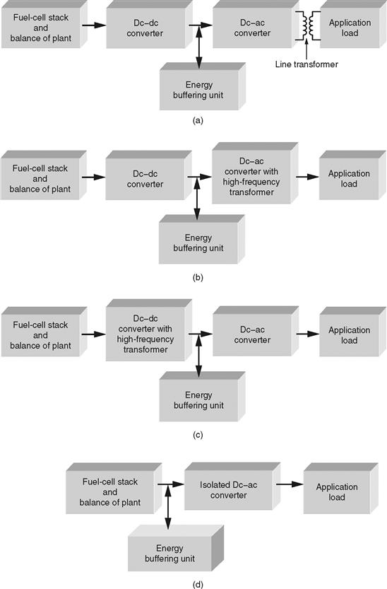
FIGURE 29.1 Inverter power-conditioning schemes [1] with (a) line-frequency transformer; (b) HF transformer in the dc-ac stage; (c) HF transformer in the dc–dc stage; and (d) single-stage isolated dc–ac converter.
29.2 Low-Cost Single-Stage Inverter [2]
Low-cost inverter that converts a renewable- or alternative-energy source's low-voltage output into a commercial ac output is critical for success, especially for the low-power applications (≤ 5 kW). FIGURE 29.2 shows one such single-stage isolated inverter, which was originally proposed in [10] as a “push-pull amplifier.” It achieves direct power conversion by connecting load differentially across two bidirectional dc–dc Ĉuk converters and modulating them, sinusoidally, with 180° phase difference. Because only four main switches are used, it would potentially reduce system complexity, costs, improve reliability, and increase efficiency. Furthermore, the common source connection between two devices both at primary (Qa and Qc) and secondary sides (Qb and Qd) makes the gate-drive circuit relatively simple. In addition, the possibility of coupling inductors or integrated magnetics will further reduce the overall volume and weight, thereby achieving lesser material and space usage. Another advantage of this inverter is the reduction of turns ratio of the step-up transformer, which is usually required to achieve rated ac from low dc voltage. The inherent voltage boosting capability of the Ĉuk inverter can reduce the transformer turns-ratio requirement by at least half. Low transformer turns-ratio yields less leakage inductance and secondary winding resistance, which reduces the loss of duty cycle and secondary copper losses, respectively.
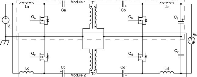
FIGURE 29.2 Schematic of the single-stage dc-ac differential-isolated Ĉuk inverter [2].
29.2.1 Operating Modes
In order to understand how the current flows and energy transfers during the switching and to help select the device rating, four different modes of the inverter are analyzed and shown in Fig. 29.3. It shows the direction of the current when the load current flows from the top to the bottom.
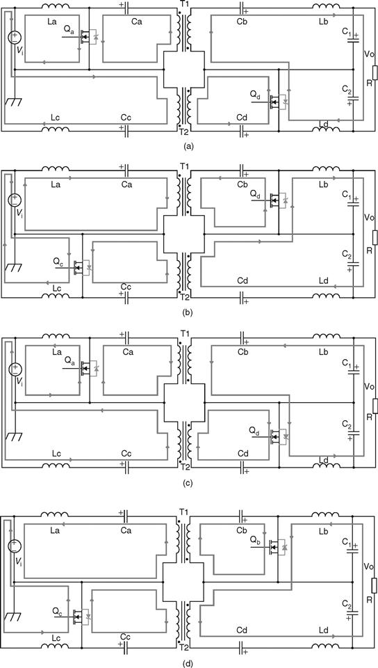
FIGURE 29.3 Direction of the current flow [2]: (a) and (b) for positive load current and (c) and (d) for negative load current, (a) Mode 1, when Qa, Qd are ON and Qb, Qc are OFF; (b) Mode 2, when Qa, Qd are OFF and Qb, Qc are ON; and (c) and (d) are Modes 3 and 4 corresponding to negative load current.
Mode 1: Figure 29.3a shows the current flow for the case when switch Qa, Qd are ON and Qb, Qc are OFF. During this time, the current flowing through the input inductor La increases and the inductor stores the energy. At the same time, the capacitor Ca discharges through Qa, and thus, there is transfer of energy from the primary side to the secondary side through the transformer T1. The capacitor Cb is discharged to the circuit formed by Lb, C1, and the load R. Meanwhile, the inductor Ld stores energy, and its current increases. The capacitor Cd discharges through Qd. The power flows in opposite direction in the Module 2 from the secondary side to the primary side. The capacitor Cc is also discharged to provide the power.
Mode 2: When Qa, Qd are turned OFF, and Qb, Qc are ON (Fig. 29.3b); Ca, Cd, Cb, and Cc are charged using the energy, which was stored in the inductors La and Ld, while Qa, Qd were ON. During this time, Lb and Lc will release their energy.
Figure 29.3c,d shows the current direction when the load current flows in the opposite direction. The description for these two modes is omitted due to the similarity with Fig. 29.3a,b.
29.2.2 Analysis
Although the nonisolated inverter has already been proposed [10], detailed analysis and design of the isolated version have not appeared in any literature. The output of the inverter is the difference between two “sine-wave modulated PWM controlled” isolated Ĉuk inverters (Module 1 and Module 2), with their primary sides connected in parallel. The two diagonal switches of two modules are triggered by a same signal (Qa = Qd and Qb, = Qc), while the two switches in each module have complementary gate signals (Qa =/Qb and Qc =/Qd). As we know, the output voltage of an isolated Ĉuk inverter can be expressed as follows:
![]() (29.1)
(29.1)
where D is the duty ratio, N is the transformer turns ratio, and Vi is the input voltage. Because duty ratios for Modules 1 and 2 are complementary, the output difference between the two modules is
![]() (29.2)
(29.2)
The curves corresponding to the terms in (Eq. 29.2) with respect to the duty ratio D (assuming N=l) are plotted in Fig. 29.4. The figure shows that although the gain-duty ratio curves of Modules 1 and 2 are not linear, their difference is almost linear. Therefore, if a sine-wave-modulated duty ratio D is used as a control signal for the inverter, then its output voltage will be a sine wave with small distortion.
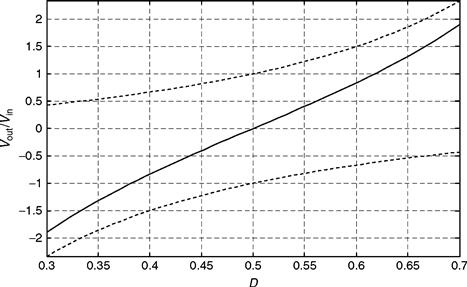
FIGURE 29.4 Voltage gain versus D [2] for Modules 1 and 2 (top and bottom), and their difference (middle).
29.2.3 Design Issues
A 1 kW single-stage isolated dc-ac Ĉuk inverter prototype was designed and tested to verify its performance for fuel cell application, where stack voltage is 36 V. Some design issues are discussed later.
29.2.3.1 Choice of Transformer Turns-Ratio and Duty-Ratio Calculation
An inverter, normally, if operating at lower range of duty ratio (i.e., lower modulation index) with output power and input dc voltage fixed will produce lower output voltage, i.e., a higher current. This results in higher conduction losses and lower efficiency. Therefore, from the efficiency point of view, an inverter should usually operate at wide range of duty ratio. However, there is a duty-ratio limitation for proper operation on the dc-ac Ĉuk inverter. Unlike dc–dc, the duty ratios of the control PWM signals are not constant but sine-wave modulated. For a given input voltage (36 V dc, for instance) and output voltage (110V ac, 60 Hz), the shape and magnitude of duty ratio (D) for dc-ac Ĉuk inverter will vary according to transformer turns ratio (N) [2]:
![]() (29.3)
(29.3)
Solving D, we obtain [2]
![]() (29.4)
(29.4)
where α = Vm · N/Vi. It is a constant value. Vm represents the amplitude of the desired output sine wave. The numerical calculation shows that term B in (Eq. 29.4) is always larger than A. Thus, A + B is always positive while A — B is negative. Therefore, only (A + B)/C is considered because D has to be a positive value. Note, when sin(wt) → 0, C → 0, and A + B → 0. In this case, D is calculated using L'Hospital's rule as [2]
![]() (29.5)
(29.5)
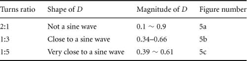
Figure 29.5 shows the plot of D = (A + B)/C for three different transformer turns ratios. The results are summarized in Table 29.1. It is clearly shown that, there is a trade-off between output voltage distortion and duty-ratio range. An optimal transformer turns ratio, N = 3, is selected with corresponding D varying from 0.34 to 0.66.
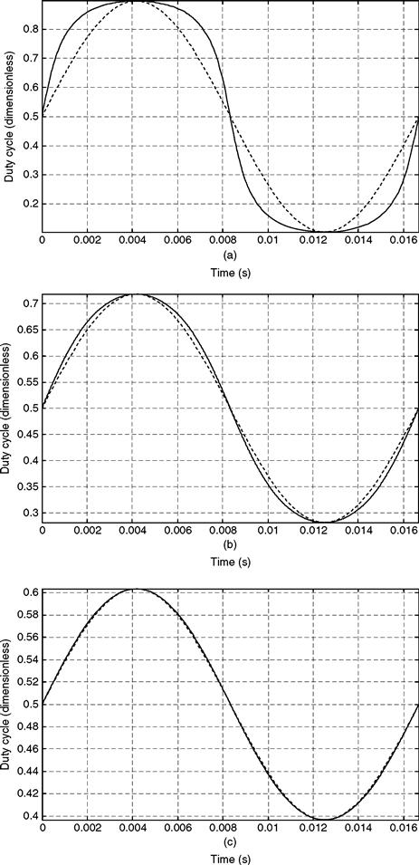
FIGURE 29.5 The plotted waveforms [2] of D = (A + B)/C for variable transformer turns ratio (solid), (a) N = 2:1; (b) N = 1:2; and (c) N = 1:5, as compared with a standard sine wave (dash).
TABLE 29.1 Shape and range of D for different transformer turns ratio
29.2.3.2 Lossless Active-Clamp Circuit to Reduce Turn-Off Losses
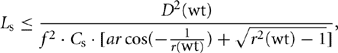
There will be severe voltage spikes and ringing across the switches during turn-off. They are caused by the transformer and other parasitic leakage inductances combined with a very high current reverse going through the transformer primary side. The spike problem is more serious at the point where the output sine wave is at its peak because of the highest instantaneous current value at that point. The circuit inside the dotted block of Modules 1 and 2 in Fig. 29.6 shows a lossless active-clamp circuit, which can achieve zero-voltage turn-off, thereby reducing the turn-off losses and limiting the maximum voltage across the main switches. The circuit for each module contains two auxiliary diodes, one capacitor, one inductor, and one switch. The auxiliary switches Ss1 and SS2 are triggered using the same gate signals as their corresponding main switches. The equations to calculate capacitance Cs and inductance Ls are listed as follows [2]:
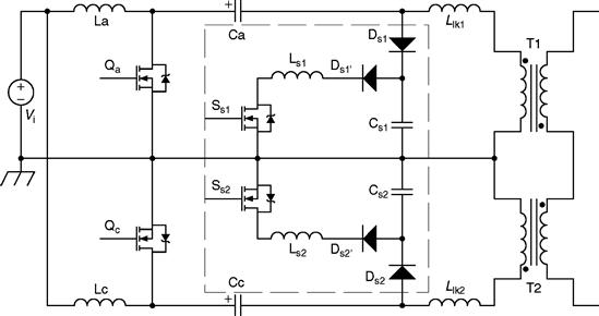
FIGURE 29.6 The single-stage Ĉuk inverter with lossless active-clamp circuit at the primary side [2].
![]() (29.6)
(29.6)
where D(wt) is the sine wave modulated duty ratio, Vo(wt) is the sine wave output, Vc max is the maximal clamped voltage, and Le is the effective inductance. With reference to Fig. 29.6, when the switch Qa turns OFF, the clamp circuit will create an alternate path formed by diode Ds1 and capacitor Cs1 to divert the turn-off current from the primary switch Qa. After switch Qa and Ss1 are turned ON, the energy stored in capacitor Cs1 will eventually be fed back to the capacitor Ca as useful power. The performance of the active-clamp circuit along with inverter performance is provided in detail in [11].
29.3 Ripple-Mitigating Inverter [3, 4]
The inverter (see Fig. 29.7) described in this section comprises a dc–dc zero-ripple boost converter (ZRBC), which generates a high-voltage dc at its output followed by a soft-switched, transformer isolated dc-ac inverter, which generates a 110 V ac. The HF-inverter switches are arranged in a multilevel fashion and are modulated by a fully rectified sine wave to create a HF, three-level ac voltage as shown in Fig. 29.7. Multilevel arrangement of the switches is particularly useful when the intermediate dc voltage > 500 V. The HF inverter is followed by the ac–ac converter, which converts the three-level ac to a voltage that carries the line-frequency sinusoidal information.
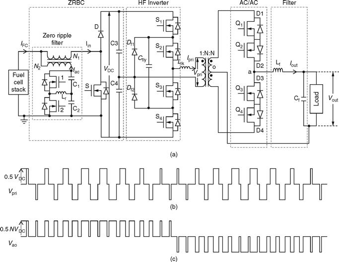
FIGURE 29.7 Schematic of the ripple-mitigating inverter [3]. The source can PV/battery/rectified wind as well.
29.3.1 Zero-Ripple Boost Converter (ZRBC)
The ZRBC is a standard nonisolated boost converter with the conventional inductor replaced by a hybrid zero-ripple filter (ZRF). The ZRF (shown in Fig. 29.8) is viewed as a combination of a coupled inductor (shown in Fig. 29.7) and a half-bridge active power filter (APF) (shown in Fig. 29.7). Such a hybrid structure serves the dual purpose of reducing the HF current ripples and the low-frequency current ripples. The coupled inductor minimizes the HF ripple from the source current (IDC+i2 = i1) and the APF minimizes the low-frequency ripple from the source current (Idc + iac = iin). IDC is the dc supplied by the source, i2 is the HF ac supplied by the series combination of identical capacitors C1 and C2 (in Fig. 29.7), and iac is the low-frequency ac supplied by the APF storage reactor Lr. For effective reduction of the HF current from the source output, the value of the capacitors C1 and C2 should be as large as possible. However, the series combination should be small enough to provide a high-impedance path to the low-frequency current iac. Therefore, for a chosen value of capacitor, the values of the following expression hold true [3]:
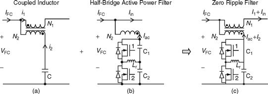
FIGURE 29.8 Schematic diagrams [3] and [4] of (a) coupled inductor structure for reducing the HF current ripple; (b) half-bridge active filter, which compensates for the low-frequency harmonic-current-ripple demand by the inverter; and (c) the proposed hybrid ZRF structure.
(29.10a) ![]()
where fHF is the switching frequency of the converter and fLF is the lowest frequency component in iac.
Assuming the switching frequency is approximately 20 times the lowest frequency component, the value of ZRF passive components L2 and Lr can be determined as follows [3]:
(29.10d) ![]()
Therefore, the value of L2 should be small in order to limit the value of Lr and also to minimize the phase shift in the injected low-frequency current iac.
In the following subsections, the HF and low-frequency ac-reduction mechanisms and the conditions to achieve the same are discussed. In addition to this, the effect of coupled inductor parameters on the bandwidth of the open-loop system will be discussed. For the purpose of analysis, the value of the capacitors C1 and C2 is assumed to be large. Hence, the dynamics of the APF is assumed to have minimal effect on the coupled-inductor analysis.
29.3.1.1 HF Current-Ripple Reduction
In this section, the inductance offered by the coupled inductor and the ripple reduction achievable is discussed. For that purpose, we need to derive an expression for the effective inductance of the coupled inductor. Because the value of the capacitors C1 and C2 is large and that of L22 is small, the dynamics of the APF is assumed to have minimal effect on the coupled-inductor analysis. The pi-model for the zero-ripple coupled inductor and the excitation voltage and the current for the primary and the secondary windings are shown in Fig. 29.9. The currents i1HF and i2HF are, respectively, the primary and the secondary ac shown in Fig. 29.9:
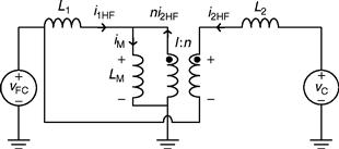
FIGURE 29.9 Ac model for the coupled inductor shown in Fig. 29.8a [3].
(29.11a) ![]()
where L11 is the self inductance of the primary winding with N1 turns. Solving (Eqs. 29.11a) and (29.11b), the expressions for ![]() and
and ![]() are obtained using
are obtained using
(29.12a) 
By substituting Eq. (29.12a) in Eq. (29.12b), we obtain the following expression:
(29.12c) 
To reduce the ac component of the source current to zero, the following condition should hold:
![]() (29.13)
(29.13)
Therefore, using the above condition and Eq. (29.12c), one obtains [3]
 (29.14)
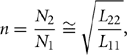
The denominator of Eq. (29.14) is the effective inductance Leff offered by the coupled-inductor structure of the hybrid filter. The effective inductance depends on the turns ratio n, the coupling coefficient k, and the self inductance L11 of the primary winding. For very small values of turns ratio (n ![]() 1), significantly large values of effective inductances can be obtained. Figure 29.10 shows the effective inductance curves and the corresponding reduction in the ripple. Figure 29.10a shows the dependence of normalized Leff on n as a function of k. For the values of effective inductance shown in Fig. 29.10a, the corresponding values of achievable ripple current in both the coupled-inductor windings are shown in Fig. 29.10b. Using Fig. 29.10b, a designer can decide on a value of HF current ripple, and using the corresponding values of n and k the normalized effective inductance can be chosen from Fig. 29.10a. While deciding the value of HF ripple, one should choose a small value for n (< 0.25) to ensure that L22 is small enough to prevent significant variations in the voltage across capacitors C1 and C2. Also, the effective inductance should be chosen to meet the bandwidth requirements of the ZRBC. Increase in the effective input inductance has a two-pronged effect on the open-loop frequency response of the ZRBC. First, the bandwidth is reduced, and second, the RHP zero is drawn closer to the imaginary axis resulting in a reduction in the available phase margin and thereby the ZRBC stability.
1), significantly large values of effective inductances can be obtained. Figure 29.10 shows the effective inductance curves and the corresponding reduction in the ripple. Figure 29.10a shows the dependence of normalized Leff on n as a function of k. For the values of effective inductance shown in Fig. 29.10a, the corresponding values of achievable ripple current in both the coupled-inductor windings are shown in Fig. 29.10b. Using Fig. 29.10b, a designer can decide on a value of HF current ripple, and using the corresponding values of n and k the normalized effective inductance can be chosen from Fig. 29.10a. While deciding the value of HF ripple, one should choose a small value for n (< 0.25) to ensure that L22 is small enough to prevent significant variations in the voltage across capacitors C1 and C2. Also, the effective inductance should be chosen to meet the bandwidth requirements of the ZRBC. Increase in the effective input inductance has a two-pronged effect on the open-loop frequency response of the ZRBC. First, the bandwidth is reduced, and second, the RHP zero is drawn closer to the imaginary axis resulting in a reduction in the available phase margin and thereby the ZRBC stability.
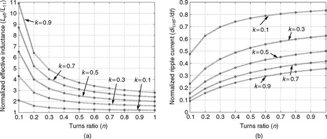
FIGURE 29.10 Normalized (a) effective inductance and (b) ripple current of the coupled inductor [3].
29.3.1.2 Active Power Filter
The input current of the inverter comprises a dc component and a 120-Hz ac component and is expressed as [3]
![]() (29.15)
(29.15)
where, Vout are inverter output voltage
Here, we derive the condition for low-frequency current ripple elimination from the PCS input current. For the APF shown in Fig. 29.8, the voltage across the storage reactor Lr of the APF is expressed as
![]() (29.16)
(29.16)
where Sa is the modulating signal. The reactor current ir is
![]() (29.17)
(29.17)
Where, ![]() and
and ![]()
![]() (Considering only the fundamental component.)
(Considering only the fundamental component.)
The current injected by the APF is
(29.18a) ![]()
In order to reduce the second harmonic in the input current to zero, iac = Iac [3]
(29.19a) ![]()
This yields
(29.19b) ![]()
29.3.2 HF Two-Stage DC-AC Converter
The two-stage dc-ac converter (shown in Fig. 29.7) comprises a soft-switched, phase-shifted SPWM, multilevel HF converter (on the primary side of the transformer) and a line-frequency-switched ac–ac converter (on the secondary side of the transformer) followed by output low-pass filter. The multilevel arrangement of the HF converter switches reduces the voltage stress and the cost of the HF semiconductor switches. The ac–ac converter has two bidirectional switch pairs Q1 and Q2, and Q3 and Q4 for a single-phase output. To achieve a 60-Hz sine-wave ac at the output, a sine-wave modulation is performed either on the HF dc-ac converter or on the ac–ac converter. Therefore, two different modulation strategies are possible for the dc-ac converter. Both schemes result in the soft switching of the HF converter, while the ac–ac converter is hard-switched.
In the first modulation scheme, the ac–ac converter switches follow SPWM, while the HF converter switches are switched at fixed 50% duty ratio. The HF converter switches in this scheme undergo zero-voltage turn-on. In the second modulation scheme, the switches of the multilevel HF converter follow SPWM, and the ac–ac converter switches are switched based on the power-flow information. Unlike the first modulation scheme, which modulates the ac–ac converter switches at HF, in the second modulation scheme, ac–ac converter operates at line frequency. The switches are commutated at HF only when the polarities of output current and voltage are different. Usually this duration is very small, and therefore the switching loss of the ac–ac converter is considerably reduced compared with the conventional control method. Therefore, the heat-sinking requirement of the ac–ac converter switches is significantly reduced. The HF converter switches in this scheme undergo zero-current turn-off. Control signals for the second modulation scheme are shown in Fig. 29.11.
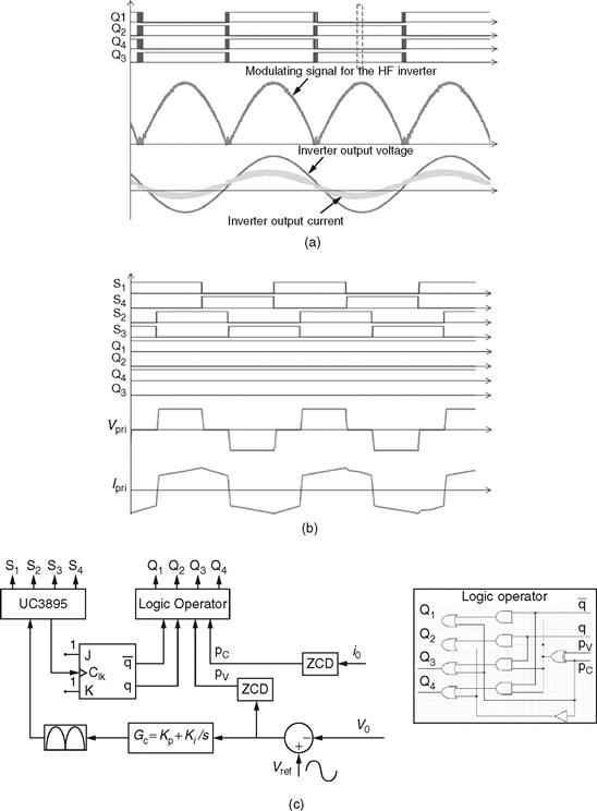
FIGURE 29.11 (a) and (b) Schematic waveforms [3] for the HF dc-ac converter on the primary side of the transformer and the ac-ac converter on the secondary side of the transformer, (c) Overall control scheme for the two-stage HF inverter.
29.4 Universal Power Conditioner [1]
This approach achieves a direct power conversion and does not use any front-end dc–dc converter. As shown in Fig. 29.12, this approach has a HF dc-ac converter followed by a HF transformer and a forced ac–ac converter. Switches (Q1-Q4) on the primary side of the HF transformer are sine-wave modulated to create a HF three-level bipolar ac voltage. The three-level ac at the output of the HF transformer is converted to 60/50-Hz line-frequency ac by the ac–ac converter and the output LC filter. For an input of 30 V, the transformation ratio of the HF transformer is calculated to be N= 13. Fabrication of a 1:13 transformer is relatively difficult. Furthermore, high turns-ratio yields enhanced secondary leakage inductance and secondary winding resistance, which result in measurable loss of duty cycle and secondary copper losses, respectively. Higher leakage also leads to higher voltage spike, which added to the high nominal voltage of the secondary necessitate the use of high-voltage power devices. Such devices have higher on-resistance and slower switching speeds. Therefore, a combination of two transformers and two ac–ac converters on the secondary side of the HF transformer is identified to be an optimum solution. For an input voltage in the range of 30-42 V, we use N = 6.5, while for an input voltage of more than 42 V, we use N = 4.3. To change the transformation ratio of the HF transformer, we use a single-pole double-throw (SPDT) relay, as shown in Fig. 29.12a,b. Such an arrangement not only improves the efficiency of the transformer but also significantly improves the utilization of the ac–ac converter switches for operation at 120/240 V ac and 60/50 Hz. For 120-V ac output, the two ac–ac-converter filter capacitors are paralleled (as shown in Fig. 29.12a), while for 240-V ac output, the voltage of the filter capacitor are connected in opposition (as shown in Fig. 29.12b). Finally, Fig. 29.13 shows the closed-loop control mechanism of the inverter for grid-parallel and grid-connected modes. It is described in detail in [1] and not repeated here.
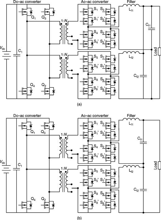
FIGURE 29.12 Circuit diagrams [1] of the proposed fuel-cell inverter for (a) 120V/60 Hz ac outputs and (b) 240V/50 Hz ac outputs. A single-pole-double-throw (SPDT) switch enables adaptive tapping of the transformer.
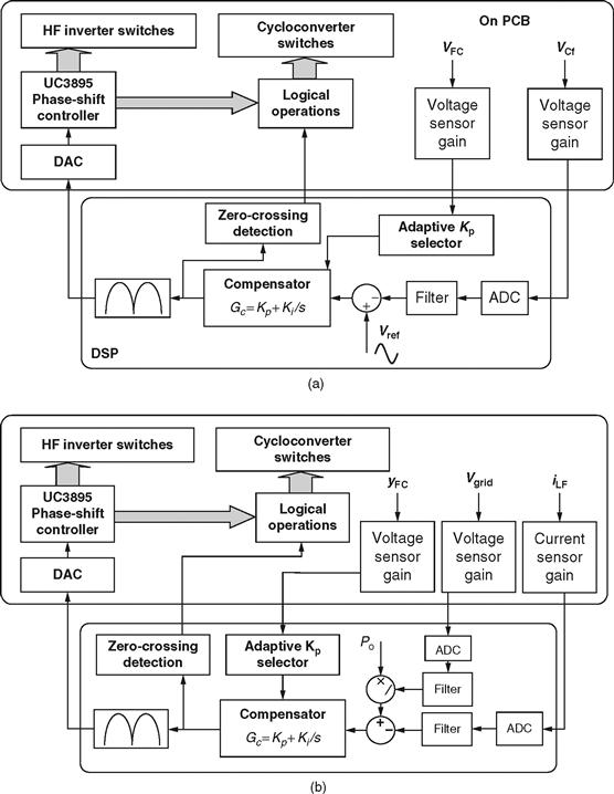
FIGURE 29.13 (a) and (b) Schematics for converter operation [1], respectively, at 120V ac and 60 Hz and 240 V ac and 50 Hz. (c) and (d) Control schemes of the inverter in grid-parallel and grid-connected modes.
29.4.1 Operating Modes
In this section, we discuss the modes of operation of the inverter in Fig. 29.12 for 120-V and 240-V ac output and for an input voltage in the range of 42–60 V (i.e., N = 4.3). The modes of operation less than 42 V (i.e., N = 6.5) remain the same. Figures 29.14 and 29.15 show the waveforms of the five operating modes of the phase-shifted HF inverter and a positive primary and a positive filter-inductor current. Modes 2 and 4 show the zero-voltage switching (ZVS) turn-on mechanism for switches Q3 and Q4, respectively. Unlike conventional control scheme for ac–ac converter [12], which modulates the switches at HF, the outlined ac–ac converter operates at line frequency. The switches are commutated at HF only when the polarities of the output current and voltage are different [12]. For unity-power-factor operation, this duration is negligibly small, and therefore, the switching loss of the ac–ac converter is considerably reduced compared with the conventional control method [13].
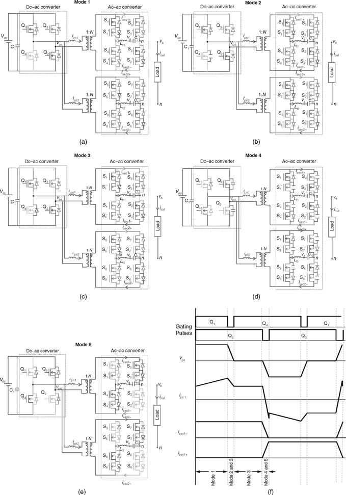
FIGURE 29.14 Modes of operation [1] for 120 V ac for input voltage in the range of 42-60 V (N = 4.3): (a-e) topologies corresponding to the five operating modes of the overall dc-ac converter for positive primary current and for power flow from the input to the load, (f) Schematic waveforms show the operating modes of the HF inverter when primary currents are positive. The modes of operation of less than 42 V (i.e., N = 6.5) remain the same.
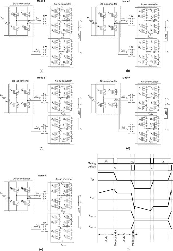
FIGURE 29.15 Modes of operation [1] for 240 V/50 Hz ac output for an input-voltage range of 42-60 V (corresponding to N = 4.3): (a-e) topologies corresponding to the five operating modes of the inverter for positive primary and positive filter-inductor currents, (f) Schematic waveforms show the operating modes of the dc-ac converter when primary currents are positive. The modes of operation of less than 42 V (corresponding to N = 6.5) remain the same.
Five modes of the inverter operation are discussed for positive primary current. A set of five modes exists for a negative primary current as well. A similar set of five modes of operation for the 240 V ac exists for input voltage of more than 42 V (N = 4.5). Again, the mode of operation for input voltage of less than 42 V (N = 6.5) remains the same.
Mode 1 (Fig. 29.14a): During this mode, switches Q1 and Q2 of the HF inverter are ON, and the transformer primary current Ip1 and Ip2 is positive. The load current splits equally between the two cycloconverter modules. For the top cycloconverter module, the load current Iout/2 is positive and flows through the switches pair S1 and S1', the output filter Lf1 and Cf1, switches S2 and S2‘, and the transformer secondary. Similarly, for the bottom cycloconverter module, the load current 0.5 × IOut is positive and flows through the switches pair S5 and S5', the output filter Lf2 and Cf2, switches S6 and S6‘, and the transformer secondary.
Mode 2 (Fig. 29.14b): At the beginning of this interval, the gate voltage of the switch Q1 undergoes a high-to-low transition. As a result, the output capacitance of Q1 begins to accumulate charge and, at the same time, the output capacitance of switch Q4 begins to discharge. Once the voltage across Q4 goes to zero, it is can be turned on under ZVS. The transformer primary currents Ip1 and Ip2 and the load current IOut continue to flow in the same direction. This mode ends when the switch Q1 is completely turned OFF and its output capacitance is charged to VDC.
Mode 3 (Fig. 29.14c): This mode initiates when Q1 turns OFF. The transformer primary currents Ip1 and Ip2 are still positive, and free wheels through Q4 as shown in Fig. 29.14c. Also the load current continues to flow in the same direction as in Mode 2. Mode 3 ends at the commencement of turn off Q2.
Mode 4 (Fig. 29.14d): At the beginning of this interval, the gate voltage of Q2 undergoes a high-to-low transition. As a result, the output capacitance of Q2 begins to accumulate charge and, at the same time, the output capacitance of switch Q3 begins to discharge as shown in the Fig. 29.14d. The charging current of Q2 and the discharging current of Q3 together add up to the primary currents Ip1 and Ip2. The transformer current makes a transition from positive to negative. Once the voltage across Q3 goes to zero, it is turned ON under ZVS. The load current flows in the same direction as in Mode 3 but makes a rapid transition from the bidirectional switches S1 and S1‘ and S2 and S2‘ to S3 and S3‘ and S4 and S4‘, and during this process Iout/2 splits between the two legs of the cycloconverter modules as shown in Fig. 29.14. Mode 4 ends when the switch Q2 is completely turned OFF, and its output capacitance is charged to VDC. At this point, it is necessary to note that because S1 and S2 are OFF simultaneously, each of them support a voltage of Vdc.
Mode 5 (Fig. 29.14e): This mode starts when Q2 is completely turned OFF. The primary currents Ip1 and Ip2 are negative, while the load current is positive as shown in Fig.29.14e.
29.4.2 Design Issues
29.4.2.1 Duty-Ratio Loss
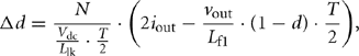
As shown in Fig. 29.16, the finite slope of the rising and falling edges of the transformer primary current because of the leakage inductance (Llk) will reduce the duty cycle (d). This duty-ratio loss is given by [1]
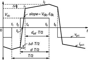
FIGURE 29.16 Transformer primary-side voltage and current waveforms [1].
 (29.20)
where N is the transformer turns ratio, Lf1 is the output filter inductance, iout is the filter current, vout is the output voltage, and T is the switching period. Assuming that Lf1 is large enough, the second term in Eq. (29.20) can be omitted. Thus, the duty-ratio loss has a sinusoidal shape and is proportional to N and L1k. One can deduce from Eq. (29.20) that, due to the high turns-ratio and low-input voltage, even a small leakage inductance will cause a big duty-ratio loss.
Figure 29.17 shows (for a 1-kW inverter) the calculated duty-ratio loss for an input voltage of 30 V and for N = 6.5. Four parametric curves correspond to four leakage inductances of 0.5, 1, 1.5, and 2 μH are shown. Figure 29.17 shows that, for a L1k of 2 μH, the duty-ratio loss is more than 25%. Consequently, a transformer with even higher turns-ratio is required to compensate for this loss in the duty ratio, which increases the conduction loss and eventually decreases the efficiency.
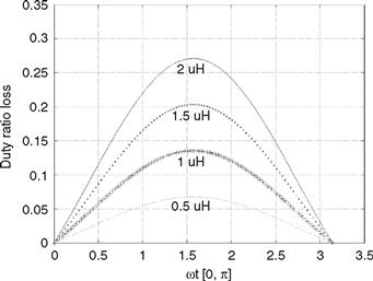
FIGURE 29.17 Variation of duty-ratio loss as a function of Llk over half-a-line cycle [1].
29.4.2.2 Optimization of the Transformer Leakage Inductance
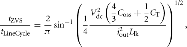
The leakage inductance of the HF transformer enhances the ZVS range of the dc-ac converter but reduces the duty ratio of the converter, which increases the conduction loss. Thus, the leakage inductance of each transformer is designed to achieve the highest efficiency, as illustrated in Fig. 29.18. For the sinusoidally modulated dc-ac converter, the ZVS capability is lost twice in every line cycle. The extent of the loss of ZVS is a function of the output current. The available ZVS range (tzvs) as a percentage of the line cycle (tLineCycle) is given by [1]
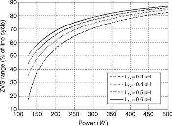
FIGURE 29.18 ZVS range of the dc-ac converter with variation in output power [1].
 (29.21)
where Coss is the device output capacitance and CT is the interwinding capacitance of the transformer. When the dc-ac converter is not operating under ZVS condition, the devices are hard-switched. A numerical calculation of the total switching losses for the 1-kW inverter, as shown in Fig. 29.19, indicates that the optimal primary-side leakage inductance for the HF transformer should be between 0.2 and 0.7 μH. Clearly, as the leakage inductance of the HF transformer increases, the total switching loss decreases due to an increase in the range of ZVS, while the total conduction loss increases with increasing leakage inductance.
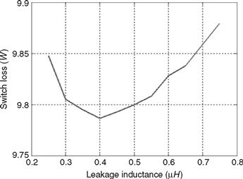
FIGURE 29.19 Variation of the total switch loss of the dc-ac converter with the leakage inductance of the HF transformer [1].
29.4.2.3 Transformer Tapping
The voltage variation on the secondary side of the HF transformer necessitates high-breakdown-voltage rating for the ac–ac-converter switches and diminishes their utilization. For a step-up transformer with N = 6.5, the ac–ac-converter switches have to withstand at least 390 V nominal voltage when input ramps to the high end (60 V), while only 195 V is required when 30 V is the input. In addition to the nominal voltage, the switches of the ac–ac converter have to tolerate the overshoot voltage (as shown in Fig. 29.20) caused by the oscillation between the leakage inductance of the transformer and the junction capacitances of the power MOSFETs during turn-off [11]. The frequency of this oscillation is determined using ![]() , where Ceq is the equivalent capacitance of the switch output capacitance and the parasitic capacitance of the transformer winding. The conventional passive snubber circuit or active-clamp circuits can be used to limit the overshoot but they will induce losses, increase the system complexity, and component costs. One simple but effective solution is to adjust the transformer turns ratio according to the input voltage.
, where Ceq is the equivalent capacitance of the switch output capacitance and the parasitic capacitance of the transformer winding. The conventional passive snubber circuit or active-clamp circuits can be used to limit the overshoot but they will induce losses, increase the system complexity, and component costs. One simple but effective solution is to adjust the transformer turns ratio according to the input voltage.
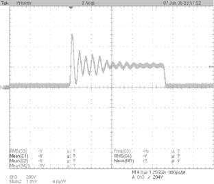
FIGURE 29.20 Drain-to-source voltage [1] across one of the ac-ac converter power MOSFETs.
To change the turns ratio of the HF transformer, a bidirectional switch is required. Considering its simplicity and low conduction loss, a low-cost SPDT relay is chosen for the inverter, as shown in Fig. 29.12. For this prototype, for an input voltage in the range of 30–42 V, N equals 6.5. Hence, 500 V devices are used for the highest input voltage considering an 80% overshoot in the drain-to-source voltage that was observed in experiments. For an input voltage of more than 42 V, N equals 4.3, and hence the same 500 V devices can still be used to cover the highest voltage as the magnitude of the voltage oscillation is reduced. The relay is activated near the zero-crossing point (where power transfer is negligible) to reduce the inrush current. Such an arrangement improves the efficiency of the transformer and significantly increases the utilization of the ac–ac-converter switches for the full range of the input voltage. However, without adaptive transformer tapping, the minimal voltage rating for the devices is given by Vdc max·N·(l + 80%) = 60· 6.5· 1.8 = 702 V. In practice, power MOSFETs with 800 V or higher breakdown-voltage ratings are, therefore, required because of the lack of 700 V rating devices. The so-called rule of “silicon limit” (i.e., Ron α BV2.5, where BV is the breakdown voltage) indicates that, in general, higher-voltage-rating power MOSFETs will have higher Ron and hence higher conduction losses. Furthermore, for the same current rating, the switching speed of a power MOSFET with higher breakdown-voltage rating is usually slower. As such, converter efficiency is expected to degrade further as a result of enhanced power loss.
29.4.2.4 Effects of Resonance between the Transformer Leakage Inductance and the Output Capacitance of the AC–AC-Converter Switches
Resonance between the transformer leakage inductance and the output capacitance of the ac–ac-converter devices causes the peak device voltage to exceed the nominal voltage (obtained in the absence of the transformer leakage inductance). This is demonstrated in Fig. 29.21. Considering N = 6.5, one can observe that the peak secondary voltage can be around twice the nominal secondary voltage. Consequently, the breakdown-voltage rating of the ac–ac-converter switches needs to be higher than the nominal value. As power MOSFETs are used as switches, higher breakdown voltage entails increased on-resistance that yields higher conduction loss. So, the leakage affects the conduction loss and the selection of the devices for the ac–ac converter. The resonance begins only after the secondary current completes changing its direction and the ac–ac-converter switches initiate turn-on or turn-off. During this resonance period, energy is transferred back and forth between the leakage and filter inductances and the device and filter capacitances in an almost-lossless manner. The current through the switch that supports the oscillating voltage is almost zero. Thus, practically, no switching loss is incurred because of this resonance phenomenon although it may have an impact on the electromagnetic-emission profile.
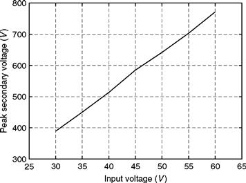
FIGURE 29.21 Peak voltage across the ac-ac converter [1] with varying input voltage for a transformer primary leakage inductance of 0.7 μH, output capacitance of 240 pF (for the devices of the ac-ac converter), and output filter inductance and capacitance of 1 mH and 2.2 μF, respectively.
29.5 Hybrid-Modulation-Based Multiphase HFL High-Power Inverter [5–8]
Recent high-voltage SiC DMOSFETs and SiC JBS diodes, with 100–400X lower on resistance and superior reverse recovery, respectively, along with projected > 3X thermal sustenance and conductivity along with advanced high-permeability and high-efficiency nano crystalline core (e.g., with > 1T flux density) transformers pave way for isolated high-power and HFL inverters. They have attained significant attention with regard to wide applications encompassing high-power renewable- and alternative-energy systems (e.g., photovoltaic, wind, and fuel-cell energy systems), DG/DER applications, active filters, energy storage, compact defense power-conversion modules for defense, as well as commercial electric/hybrid vehicles because of potential for significant reduction in materials and labor cost without much compromise in efficiency. Along that line, a new innovation in the form of a hybrid modulation (HM) [5, 6] has been put forward by the author recently that significantly reduces the switching loss of HFL topologies (e.g., Fig. 29.22 [5–8]). The HM scheme is unlike all reported discontinuous-modulation (DM) schemes where the input to the final stage of the inverter is a dc and not a pulsating-dc; further, in the HM scheme, switches in two legs of the ac–ac converter do not change state in a 60° cycle, and switches in any one leg do not change state for an overall 240°. In contrast, for a conventional DM scheme, most switches of one leg of the ac–ac converter do not change stage in a 60 or 120° cycle. The present three-phase HM scheme is also different from earlier reported modulation schemes for single-phase, direct-power-conversion systems. The primary role of the modulation scheme for the single-phase ac–ac converter is to demodulate the rectifier output on a half-line-cycle basis to generate the output sine-wave-modulation pattern by switching all the ac–ac converter devices under low-frequency condition.
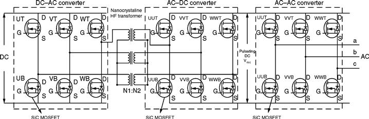
FIGURE 29.22 Schematic of the HM-based HFL topology. A conventional fixed-dc-link (FDCL) topology has the same architecture except that it has a filter capacitor after the ac-dc rectifier stage, and hence, the output ac-ac converter is fed with a dc voltage rather than a pulsating dc voltage (Vrec) for the HFL scheme. The HM scheme is implemented for the ac-ac converter stage. For the FDCL topology, the output stage is a voltage source inverter (VSI), which is operated using SVM scheme.
29.5.1 Principles of Operation [13]
29.5.1.1 Three-Phase DC-AC Inverter
Figure 29.23 illustrates the generation of switch-gate signals for the proposed converter. The bottom switches are controlled complimentarily to the upper ones, hence they are not described further. Three gate-drive signals UT, VT, and WT for primary side devices are obtained by phase shifting a square wave with respect to a 10-kHz square wave signal Q (shown in Fig. 29.24b). Q is synchronous with a 20-kHz saw-tooth carrier signal, shown in Fig. 29.24a. The phase differences are modulated sinusoidally using three 60 Hz references a, b, and c, respectively. Two gate signals for phase U and V are plotted in Fig. 29.24c and d. Because carrier frequency is much higher than the reference frequency, UT, VT, and WT will be square wave with the frequency of 10 kHz, and their phases are modulated. The obtained output line-line voltages at the primary side of the transformers are bipolar waveforms. Vuv is plotted in Fig. 29.24e as an example. After passing through HF transformers, they are rectified by a three-leg diode bridge at the secondary side to obtain a unipolar PWM waveform, which has six-pulse as envelop. Its waveform is shown in Fig. 29.24g, and the mathematic expressions are:
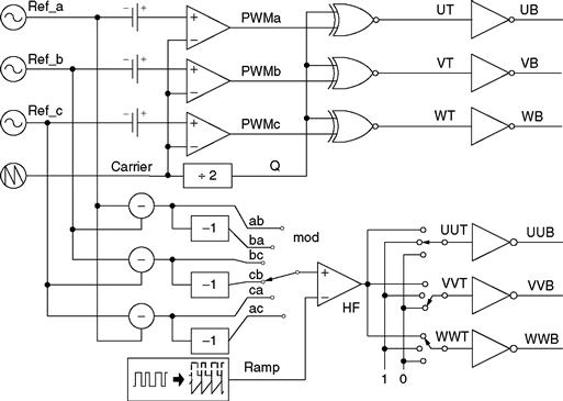
FIGURE 29.23 Diagram of gate-drive-signal generation for the HFL inverter [13].
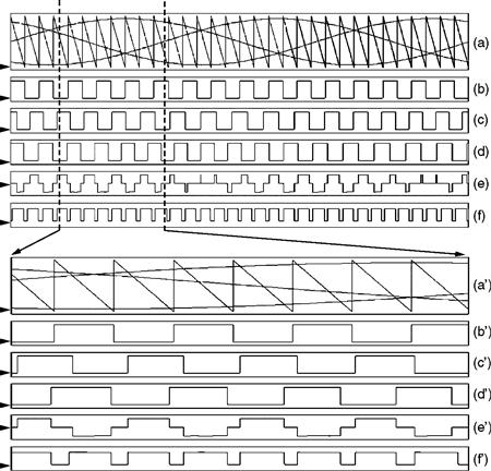
FIGURE 29.24 Key waveforms [13] of the primary-side dc-ac converter in one cycle and enlarged view of the interval between two dot lines; (a) three-phase sine-wave references and carrier signal; (b) Q: square ware with half frequency of the carrier; (c) UT: gate signal for the upper switch of phase U; (d) VT: gate signal for the upper switch of phase V; (e) Vuv: output of phase U and V; and (f) Vrec: output waveform of the rectifier.
![]() (29.22)
(29.22)
where PWMX (x = a, b, or c) denotes the binary comparator output between reference and carrier for phase x. Symbol “⊗” stands for XNOR operation. N is the transformer turns ratio. Divide the six-pulse rectified waveform into six segments named P1~P6 as shown in Fig. 29.25g. The rising and falling edges of Vrec are different for different segments. Figure 29.24a'-f' show a particular time interval within segment 2, where the rising and falling edges of Vrec (marked as ↑Vrec and ↓Vrec) are determined by the edges of UT and VT, respectively. Other cases are summarized in Table 29.2.
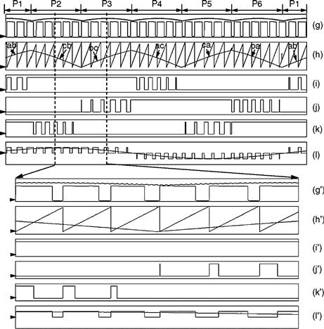
FIGURE 29.25 Key waveforms [13] of the secondary-side ac-ac inverter in one cycle and enlarged view of the interval between two dot lines; (g) Vrec: output PWM waveform of rectifier with six-pulse envelop; (h) mod: modulated signal and ramp: the carrier which is synchronous with (g); (i) UUT: gate signal for the top switch of phase a; (j) VVT: gate signal for the top switch of phase b; (k) WWT: gate signal for the top switch of phase c; and (1) PWM output of the line-line voltage Vab and its envelop.
TABLE 29.2 The edge dependence of the rectifier output on gate signals
29.5.1.2 Switching Strategy for the AC–AC Converter
Similar to the case of three-phase ac-dc rectifier, the rectified PWM output is contributed respectively by Vwv, Vuv, Vuw, Vvw, Vvu, and Vwu at each segment from P1 to P6. The bottom part of the Fig. 29.23 shows the diagram of generating switching signals for three upper switches of secondary-side ac–ac inverter. During each segment, every switch will be either: permanently ON (1), permanently OFF (0), or toggling with 20 kHz. The switching pattern for the upper three switches in each segment for one cycle period is summarized in Table 29.3.
TABLE 29.3 Switching pattern for upper switches of the ac-ac inverter
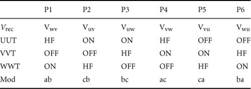
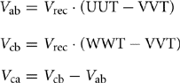
The switch positions illustrated in Fig. 29.23 are for the case of segment P2. Because the rectifier output has the same shape as Vuv within this interval, the line-line voltage Vab at the output side of the ac–ac inverter can be directly obtained by keeping switches UUT and VVT at ON and OFF status, respectively. Another line-line voltage Vcb, however, needs to be achieved by operating switches on the third leg WWT and WWB under HF condition, where modulated signal (mod) is the difference between references c and b and the carrier signal (ramp) is a 20-kHz saw-tooth waveform synchronized with the PWM output of the rectifier. The key waveforms are shown in Fig. 29.25. The mathematical expression for three line-line voltages is given as follows:
 (29.24)
An illustration of the ac–ac converter's HM scheme (as compared with several other SVM and SPWM schemes) is shown in Fig. 29.26. The outlined switching strategy is the best option for resistive load because the peaks of the currents follow the peaks of the fundamental voltages. Therefore, each phase leg does not switch just when the current is at its maximum value, thereby minimizing switching losses. For unity-power-factor load, the HM scheme for the ac–ac converter can be adjusted accordingly for minimizing the losses.
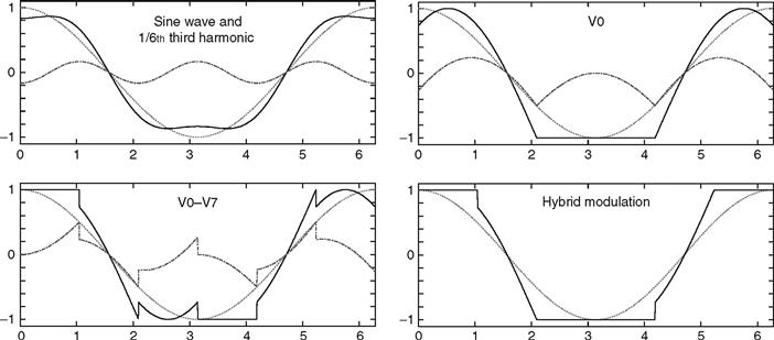
FIGURE 29.26 Modulation functions corresponding to sine wave (with l/6th third harmonic), V0, V0-V7 SVMs, and HM schemes. Blue and red traces represent zero sequence and sinusoidal signals. Black trace is the modulating signal.
Acknowledgement
The work described in this chapter is supported in parts by the National Science Foundation (NSF) under Award Nos. 0725887 and 0239131, by the Department of Energy (DOE) under Award No. DE-FC2602NT41574, and by the California Energy Commission (CEC) under Award No. 53422A/03-02. However, any opinions, findings, conclusions, or recommendations expressed herein are those of the authors and do not necessarily reflect the views of the NSF, DOE, and CEC.
Copyright Disclosure
Publication in this chapter (for educational purposes) is covered in part by earlier or to-be-published IEEE publications of the author and the IEEE sources have been referred in the chapter.
REFERENCES
1. Mazumder SK, Burra R, Huang R, Tahir M, Acharya K, Garcia G, Pro S, Rodrigues O, Duheric E. A high-efficiency universal grid-connected fuel-cell inverter for residential application. IEEE Trans. Power Electronics. 2010; vol. 57(no. 10):3431–3447.
2. Mazumder SK, Burra RK, Huang R, Arguelles V. In: A low-cost single-stage isolated differential Ĉuk inverter for fuel cell application. 2008: 4426–4431.
3. Mazumder SK, Burra RK, Acharya K. A ripple-mitigating and energy-efficient fuel cell power-conditioning system. IEEE Trans. Power Electronics. July 2007; vol. 22(no. 4):1437–1452.
4. S. K. Mazumder, R.K Burra, and K. Acharya, “Power conditioning system for energy sources,” USPTO Patent 7,372,709 B2, awarded in May 13, 2008.
5. Mazumder SK. In: A novel hybrid modulation scheme for an isolated high-frequency-link fuel cell inverter. 2008: 1–7. [doi:10.1109/PES.2008.4596911].
6. S. K. Mazumder and R. Huang, “Multiphase converter apparatus and method,” USPTO Patent Application US2009/0196082 A1, filed by University of Illinois at Chicago, 2009.
7. Huang R, Mazumder SK. A soft switching scheme for multiphase dc/pulsating-dc converter for three-phase high-frequency-link PWM inverter. IEEE Trans. Power Electronics. 2010; vol. 25(no. 7):1761–1774.
8. Huang R, Mazumder SK. A soft-switching scheme for an isolated dc/dc converter with pulsating dc output for a three-phase high-frequency-link PWM converter. IEEE Trans. Power Electronics. 2009; vol. 24(no. 10):276–2288.
9. Mazumder SK, Huang R. In: A high-power high-frequency and scalable multi-megawatt fuel-cell inverter for power quality and distributed generation. 2006: 1–5.
10. Middlebrook RD, Ĉuk S. Irvine, CA: TESLACO; 1983.
11. Pomilio JA, Spiazzi G. In: Soft-commutated Ĉuk and SEPIC converters as power factor pre-regulators. 1994: 256–261.
12. Kawabata T, Komji H, Sashida K. In: High frequency link dc/ac converter with PWM cycloconverter. 1990: 1119–1124.
13. Deng S, Mao H. In: A new control scheme for high-frequency link inverter design. 2003: 512–517.