
44
Packaging and Smart Power Systems
Dir.—Electronic Power and Energy Research Laboratory, University at Buffalo, 332 Bonner Hall, Buffalo, New York, USA
44.1 Introduction
44.2 Background
44.3.1 Steps to Partitioning
44.4 Assessing Partitioning Technologies
44.6 Technology-driven Partitioning
44.7 Example 2.2 kW Motor Drive Design
44.7.1 User Requirements (Constraints)
44.7.2 Component Characterization Map
44.7.3 Component Grouping
44.8 High Temperature (HT) Packaging
44.8.1 HT Materials Selection
44.8.2 Module Construction
44.1 Introduction
A continual endeavor in power electronics is to increase power density. This is achieved by shrinking component size, moving components closer, and reducing component count. During the last two decades, circuit frequencies increased sharply to shrink component dimensions. Improved thermal management and physical packaging materials brought components closer, and finally, increased integration of functions at the semiconductor and package levels reduced component count. This has been marked in the microelectronics world by “system on chip” (SOC), “system in package” (SIP), and “system on package” (SOP) with subsystems including “stacked die” and “multichip modules” (MCMs), all addressing higher densities and all applicable to lower power, power electronic systems.
The approach of “functional integration” has been ongoing for decades. Until the 1980s, nearly all such integration was done at the packaging level melding control and power processing. The term “smart power” (within the context of power electronic conditioning) applied in the 1960s− 1970s to the integration of computers and microprocessors into large rectifier and converter cabinets. With the advent of high-voltage-silicon integrated circuits, more functionality was brought directly to the power semiconductors, and in the 1980s− 1990s the term applied mostly to smart power semiconductors. In the late 1990s, there was a move back to hybrid integration following the trend to SOP. During the 1980s− 1990s “smart power” also became associated with digital control of higher power systems, such as motor drives and uninterruptible power supply (UPS) systems and became commercially associated with power management circuits. The first decade of the twenty-first century has ushered in “digital power” for direct control of high-frequency inner control loops in power supplies. Smart power is now more generically used since the cost of digital controllers, such as microcontrollers and programmable ICs (pics), are low cost and easily used throughout the power electronic systems.
From a designer's perspective, “functional integration” exists in a packaging continuum with “smart power” as a subset dependent on the definition in vogue. To take advantage of “functional integration” the designer, in reverse thinking, partitions or modularizes circuits, and functions to achieve the most cost-effective approach that meets a set of required performance specifications. This chapter provides background information, framework, and procedures to produce partitioning and functional integration.
44.2 Background
Circuits are typically designed based upon a pre-determined set of packaging technologies ranging from silicon integration of sub-circuit functions to multiple boards in a rack. Partitioning a circuit for packaging in one technology, such as all silicon, is straightforward. Partitioning for multiple technologies is much more difficult since higher performing technologies duplicate the aspects of lower technologies. The duplication geometrically increases parameter trade-offs and complicates design. A study on the status on power electronics packaging (STATPEP) [1] identifies metrics to evaluate the relative technical merits of the technologies.
To optimize the use of multiple technologies in functional integration, a structured method should be used. A full-cost model for various technologies is used as a basis to produce a comparative cost diagram. The diagram allows intermixing of high and low performance technologies based on surface density, which is interpreted as circuit area and, hence a partition. An example is given in Section 44.7 to demonstrate the method using a 2.2 kW motor-drive module product.
The method is also applied to product modularization, i.e. system partitioning where a specific function is used across several products. A module can represent functional integration within a packaging technology or use multiple packaging technologies to create integrated power modules (IPMs) or power electronic building blocks (PEBBs). The importance of modularization is to increase the product volume to lower cost. The cost model includes variations based on volume.
This partitioning approach matches user requirements to “Levels of Packaging” as defined in the “Framework for Power Electronics Packaging”[2] and provides optimum integration of packaging levels for a product. The framework also identifies critical technical issues that need to be considered in evaluating technical performance. This partitioning approach looks at electrical, magnetic, thermal, and mechanical issues (multiple energy forms).
44.3 Functional Integration
Figure 44.1 shows a 2.2 kW ac motor drive. Functional integration requires that the system should be partitioned both electrically and physically. The systems integrator is usually an electrical designer and the first partitioning is usually electrical. The electrical partitions and distributed power losses are also shown in the figure. The physical partitioning, or packaging, involves different components with different functions ranging from fine-line control to high-current, high-loss power processing. Several partitions can be pursued. The line-communications and motor-control blocks can use a signal-level packaging approach, such as all-silicon application-specific integrated circuit (ASIC), or discrete components on an epoxy-glass flame resistant 4 (FR-4) or insulated-metal substrates (IMS). If the power supply and control blocks are to be combined, a surface mount technology (SMT) approach cannot accommodate bulky storage components in the power supply. Hence, a through-hole approach is considered for part or both blocks. Regardless, such trade-offs can be nearly endless.
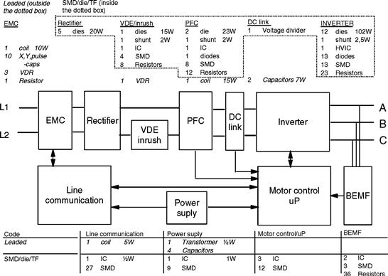
FIGURE 44.1 Block diagram of a 2.2 kW motor-drive module.
A structured method needs to be used to establish essential requirements and guide circuit and system partitioning. The method described here is based on characterizing and grouping the components, evaluating the cost and technical constraints, and then, matching packaging technologies to the groupings. All this is set against a set of comprehensive user requirements.
44.3.1 Steps to Partitioning
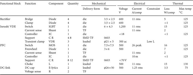
A first step to partitioning is creation of a comprehensive categorized list of electrical, mechanical, and thermal, technical user requirements. The second step is creation of a simple component characterization map that identifies dominant attributes of the components. The block diagram of a 2.2 kW motor drive is shown in Fig. 44.1 and a partial characterization map is given in Table 44.1. The map is divided into metrics by energy form to categorize and record extreme operating values for each component. Not all blocks need to be completed or components included, only those that most impact the technology selection. For example, any 5 V, < 0.1 W resistor in the control circuit need not be listed since it is accommodated by nearly all technologies (e.g. as 0806, SMT, plated through holes (PTH), thick film, etc.). For each of the remaining components, all the mechanical package formats should be listed under the delivery form.
TABLE 44.1 Component characterization map (partial listing)
The third step is to strategically group components by delivery form taking into consideration limits on electrical and thermal operating points. This first-cut grouping brings a high level of packaging integration to the system and is a critical step. Similar components from all parts of the circuit become associated.
The fourth step uses the user requirements as constraints along with the engineering experience to re-associate components into different groupings. Not all components are easily regrouped. The unassociated components become dominant factors during technology selection. As an example, the high-voltage components of a bootstrap gate-drive supply can be associated with the gate-drive circuit board or the high-voltage power inverter components. Interestingly, most unassociated components reside at the interfaces between functional blocks (as shown in Fig. 44.1).
The fifth step is to map the groupings of components to the packaging technologies. This was partially performed in the previous step as engineering judgment guided the regrouping. Refinement of the selection comes when the unassociated components are incorporated. Steps four and five become iterative to provide optimum partition(s).
44.4 Assessing Partitioning Technologies
To better understand the correlation between electrical and physical circuits (partitioning and packaging), consider the morphology of a generic circuit. A circuit has three partitions: components, topologies, and controls. Components are active or passive, such as ICs or heat sinks. Topologies are the positioning of the components to provide a function, such as a buck converter or the thermal structure of silicon soldered on copper clad to ceramic. Controls provide a preferred set of rules for operation of those components, such as voltage regulation or a thermostatically controlled fan. Hence, a “circuit” design involves electrical and physical design. The physical design is packaging and can be defined as
“… the art (design) of arranging components to provide a function or characteristic”
Note that packaging is a design function, whereas manufacturing embodies the processes to fabricate the designed arrangement. Although packaging and manufacturing are strongly interrelated, they are not synonymous.
The term “physical” should be further defined. The term “Electrical” identifies the form of energy being processed. Hence, “physical” represents other forms, such as mechanical, thermal, chemical, photonic, etc. The power electronics designer is mostly interested in electric, magnetic, mechanical, and thermal. Discussion will be limited to these four energy forms.
An integrated design problem example relating the four energy forms of interest is as follows. A high-frequency magnetic core couples the radiated field into a copper conductor on a printed wiring board (PWB) and causes eddy current heating, increasing the skin-effect resistance. Higher resistance loss further increases conductor heating which increases the mechanical stresses between the conductor and PWB leading to early failure. Who would notice the problem first? The electrical designer through circuit loss measurements; the thermal designer through a thermograph of that specific spot, or the packaging engineer who first notices the conductors are lifting off the board and assumes the conductor adhesion is poor because of faulty chemistry?
44.4.1 Levels of Packaging
The Levels of Packaging divides a system, top-down, into lower and lower subassemblies with the boundary drawn between assembly and subassemblies as shown in Fig. 44.2.
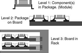
FIGURE 44.2 Levels of packaging.
Each level is defined and numbered, bottom−up, in a micro-to-macro manner. Three traditional levels in electronic packaging [3] are also applicable to power packaging. Note that levels are not easily defined. Some packages may be categorized in either of the two levels depending on the application.
Level-0: Component(s). This is the base level for a component that a designer can obtain and may be a passive, discrete semiconductor or integrated circuit, including a “smart power” circuit. The semiconductors and ICs are typically Silicon (Si), though there is significant development in SiC and GaAs for higher operating temperature and speed.
Level-1: Component(s) in Package. This is basic component packaging. Examples include mount-down and lead-attach of acomponent or semiconductor in a discrete package, or multiple components in a module. Traditional “chip and wire” hybrid circuits mounted in a housing (often, hermetic) are Level-1 packages. The package provides a “self contained environment” that allows the components to be tested, transported, and used at the next higher level of packaging while buffering electrical, mechanical, and chemical discontinuities from the next level. This package becomes a subassembly to the next higher level.
Level-2: Package on Board or Board-Level Assembly. These boards carry mixed-technology components (capacitors, resistors, inductors, and packaged discretes) that are usually coated and terminated with a connector. Examples are printed circuit board (PCB), IMS, and SMT boards. They differ from Level-1 in the lesser sophistication in fabrication. The board provides a functional partition and is a subassembly to the next packaging level.
Level-1.5 (half-level): Chip on Board (COB). This mounts “chip and wire” semiconductors directly to a PCB or on IMS. A driver in packaging is to combine levels. An objective of the road map will be the development of a direction to combine levels.
Level-3: Board in Rack or Box-Level Assembly. At this level the rack or case is considered. Each board or module is a subassembly connected to a rack backplane, motherboard, or free-wired together. An example is the output modules in a multi-output power supply. The sub-module approach provides flexibility and fast assembly time.
Definition of levels can continue into Level-4: Rack in Cabinet and Level-5: Cabinet in Room or Multiple Cabinet Level. Note that all the technical issues of packaging, embodied in passing energy across an interface or along a pathway, are the same for all levels of packaging.
44.4.2 Technologies
The delivery form, i.e. mechanical support structure for integrating functions, divides the technologies. The simplest delivery form is a mono-material approach, such as a silicon integrated circuit. A thick-film hybrid uses ceramic-glass structures to create functions. A glass-epoxy board (FR-4) allows the attachment of discrete components to “integrate functions.” Functions are not restricted to electrical, but may include magnetic, mechanical, and thermal.
The delivery form is important since the size of the mounted components greatly limits the choices in technologies. The greater the mass of the components, the more mechanically robust the technology needs to be. The technologies reviewed below belong to packaging Level-0 through Level-2 and, generally, sequentially range from fully imbedded components as in silicon ICs to modestly robust for surface mounted components, to very robust for clamped, screwed, and axially leaded. The transition from PTH to SMT occurs within FR-4 and partly explains the greater acceptance of this versatile technology.
Semiconductor Power Integrated Circuits − This is considerably different from the remaining packaging technologies in which it approaches a “mono-material system.” Multiple functions can be produced in one material, usually silicon. This is expanded in the following section.
Thick Film on Ceramic (TFC) − Glass-based pastes or inks are loaded with electrically conductive materials, such as copper, gold, or silver, to form interconnects, loaded with resistive materials to form components, or used unloaded as dielectrics. The pastes are screen printed on ceramic and fired at ~900°C. Vias are formed as holes in dielectric layers and discrete components are surface mounted with solder or adhesives. Only two types of air-fired thick film are considered here: multilayer thick film (TF-multilayer) for control circuity and thick thick-film (TTF) where silver is printed to form up to 160 μm conductors for power.
Cu Plated on Ceramic (CuPC) − Patterns are imaged or transferred to the surface of ceramic. Copper is then plated to a thickness < 125 μm (5 mils). Discrete components are attached or full thick-film processing is placed on the plated copper with screen-printed components imbedded or discrete components attached.
Glass-epoxy with Surface Mount Pads (FR-4, SMT) − A fiberglass mesh is impregnated with epoxy and metalized with copper. Interconnect patterns are etched into the foil. The patterned copper clad mesh can be laminated and vias formed by drilled and plated holes. Chip components are “surface mounted” with solder attachment or conductive polymer. Components can also be imbedded using loaded polymers similar to the TFC process, but with low temperature curing. (SMT is “surface mount technology.”)
Insulated Metal Substrate − Polymer on Metal (IMS-PM) − A polymer is used to isolate and attach a conductive interconnect to a metal plate which provides mechanical support. Vias can be placed between the interconnect and plate, and a layer of polymer and interconnect can be attached to the interconnect layer.
Insulated Metal Substrate − Steel Corded (IMS-PS) − A high temperature (HT) glass (~ 900°C) coats a steel plate and a thick-film conductive cermet interconnect is applied upon the glass. The structure is similar to traditional thick film. Vias are processed as in multilayer thick film.
Direct Bonded Aluminum (DBA) − Aluminum foil is bonded to, or cast onto ceramic, patterned, and etched. Low-resolution patterns can be direct cast. Discrete components are surface mounted with solder or adhesive. There are no vias. This is an excellent approach for Al bearing substrate materials.
Direct Bonded Copper (DBC) − Copper foil is applied to ceramic, bonded at ∼ 1063°C, and a pattern is etched. Discrete components are surface mounted with solder or adhesive. There are no vias.
Glass-epoxy with Plated through Holes (FR-4, PTH) − Same as above FR-4 except leaded components are solder attached with leads placed through holes. (PTH is “plated through holes.”)
Molded Interconnect Device (MID) − A HT plastic or polymer structure hosting electrical interconnects is fabricated by 1-shot, 2-shot, or insert molding. The interconnections are formed by hot-stamping copper foil, imaging and metal plating the polymer, or insert molding of structured metal. The MID lends itself to high volume, 3D, net shape packaging and is extensively overlooked in the power electronics area (excluding automotive). Components can be surface mounted or through-hole with moderate to course line resolution. Only the hot embossing is considered here.
Comparison of technologies

Laminated Bus-bar − A polymer, such as epoxy, glues together thick conductor bars while providing electrical isolation. The bars can be free-floating laminated interconnects or, if sufficiently thick, be the metal carrier. Vias between layers are metal posts or fasteners placed through drilled or stamped holes. These are used in high-current systems and can accommodate very large components. These were not considered in this development.
44.4.3 Semiconductor Power Integrated Circuits
As noted in the Introduction, the term “smart power” has been used for several decades to describe the imbedding of control into power processing systems. One approach integrates control and power into a monolithic circuit, such as silicon, and takes on two forms. One is the integration of analog and digital circuitry with discrete power devices. The second applies to high-voltage ICs used for power monitoring and fault control. The term “smart power” has become synonymous with power integrated circuits (Power ICs) or application-specific power ICs (Power ASICs). Motorola trademarked the term “SMARTpower” circa 1980.
A designer typically is a user of power ICs and seldom influences the chip design. systems partitioning, as described throughout this chapter, is not directly applicable. However, once the chip is available, the designer is armed with a more functionally integrated component. A background to power ICs is given below to aid the designer in better understanding the technology. An excellent reference noting the beginning of high-voltage ICs is an IEEE Press Book by B. J. Baliga [4].
Power ICs can be divided into four groups resulting from a matrix of low and high voltage, and low and high current capabilities as identified in Table 44.2. The low-voltage, low-current ICs are readily available for the control and monitoring of power processing functions. These smart chips control power supplies, battery chargers, motor drives, etc. and are often referred to as “power controllers.” These chips are produced from standard IC processes and limited to the voltages of the process. The cost follows typical IC cost structures.
TABLE 44.2 Examples of power ICs (smart power)
| Low current | High current | |
| Low voltage | Power control ICs | Bipolar drivers |
| PWM controllers | Automotive actuators | |
| High voltage | Bridge gate drivers | (limited application) |
| Gas-display drivers |
Low-voltage, low-current ICs can be further subdivided into “dedicated” and “programmable” chips. In the late 1990s and early 2000s, the incorporation of imbedded control expanded the definition of “power controllers.” Sophisticated control algorithms that were implemented in digital signal processors (DSPs) were incorporated into programmable power controllers. The role of the power electronics designer further changed to become adept at high-performance programming.
Low-voltage, high-current power ICs again use standard IC processes for fabrication. The higher current requirement is met by creating effectively large device areas that maintain current densities consistent with process characteristics. In the 1970s and 1980s, bipolar processing was dominant and large area devices were fabricated. Typically, processes were limited to 40 V and pushed to 60 V for actuator and transistor driver applications. As a side note, the most successful power metal-oxide semiconductor FET (MOSFET) driver in the 1980s used a commercially available digital “line driver” IC. Driver chips were later developed with FET processes that paralleled many low-power FET cells. Again, the required area was determined by the maximum current density of the allowed process.
Dedicated chips of the 1990s used power MOSFET technology to create driver and actuator chips. Applications of the low-voltage, high-current ICs fall mostly in the areas of power conditioning for photovoltaic systems, actuators for computer hard drives, actuators and motor drives for automotive and appliance applications, and driver applications in power semiconductors circuits.
Since mostly all IC technology was created for computer and telecommunications applications, creation of “higher voltage” ICs for power was slow to develop. Lack of market size in power did not support substantial technology development, but rather incremental product development. However, high-voltage ICs were developed early on for the gas-tube display market (circa. 1980s). Other significant developments slowly occurred mostly in drivers for power-bridge circuits as used in motor drives and “application specific ICs.”
High-voltage ICs are processed with either dielectric isolation or junction isolation. In the 1980s, dielectric isolation was used extensively by Dionics Incorporated for display drivers which had ratings of several hundred volts. Dielectric isolation utilizes silicon-dioxide wells. Devices, such as bipolar transistors, are fabricated in the wells, which serve as functional islands. The devices are then interconnected at the surface.
Limitation of the dielectric isolation process is the higher cost. However, dielectric isolation does provide for more reliable isolation with greater circuit flexibility. Both power rating and current capacity are low relative to junction isolation because of the planar nature of the structure and interconnects.
Junction isolation became the preferred method starting in mid-1990s with the developments from General Electric and Harris companies followed by power-ASICs from power semiconductor manufacturers. The isolation method used multiple levels of p−n junctions to form wells. A cross section of several basic technologies is shown in Fig. 44.3. Note the p-type sinkers connecting to the p-material of the substrate to provide cell isolation. There is also a combination of structures used to produce a BiCMOS process. The complementary metal-oxide semiconductor (CMOS) provides the control circuitry while the bipolar structures provide high current-density transistors for power processing.
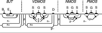
FIGURE 44.3 Junction isolation used to separate devices or circuits.
Junction isolation has several limitations, most significant of which is possible “layer inversion.” Inversion occurs when the reference substrate, or portions thereof, becomes reversed biased. Relatively large currents can flow and biasing of four layer structures can cause latch-up. Manufacturers have paid significant attention to minimizing this problem. However, designers must always be cautious that a fault condition or capacitive current from a high-frequency transient does not induce an inversion.
44.5 Cost-driven Partitioning [5]
This is the one issue seldom discussed in open literature, yet is the greatest driver to the selection of circuit design approaches and determination of partitions. Unfortunately, a designer often limits cost estimation to only component cost, i.e. the bill of materials (BOM). The greatest cost is often not the component, but the handling, mounting, and testing of a component. An excellent example is the selection of output filter capacitors in dc−dc supplies. The use of a multitude of smaller ceramic chip capacitors, which can be automatically surface mounted, is often less expensive than larger electrolytic through-hole-mounted capacitors, and provide much greater reliability over time. (This applies to larger volume production.)
The use of cost-driven partitioning is also dependent on the company structure. A vertically structured company with captive manufacturing has the advantage of increasing volume by modularizing their circuits to be used across several product lines. The following procedure uses a Full-cost Model applicable to both captive and out-sourced manufacturing.
When discussing cost, it is necessary to define centers of cost for both the product and the business. The terms are defined as follows.
1. Materials cost represent direct costs of packaging, and include the minimum packaged component (e.g. silicon chip), component packaging materials (e.g. plastic housing on a TO-220), and packaging materials for manufacture (e.g. solder or adhesives for mount down). If the manufacturer can mount bare die, then these quantities are determined separately. If manufacturing is out-sourced, then the “pre-packaged” component cost accounts for the first two costs and the manufacturer (or assembler) determines the third cost. The variation in cost by volume must also be included. Volume dependency is greatest for custom products at low volume and lowest for standard high-volume products. A typical volume cost factor is 20% decrease in cost per 10-fold increase in volume.
2. Production cost includes factors for wages and product volume, but are independent of material costs, (which is not often assumed when assessing overhead). Production cost can be characterized as a function of technology and quantity. To reflect this into a design tool, it is necessary to describe production cost as a function of simple information, such as the number of surface mount device (SMD) and leaded components, and square inches of substrate board. Assessment is as follows for captive production:
1. Determine the total wages, equipment and facility depreciation, and other facility overhead.
2. Determine the number of production technologies in the facility, both in place and available with minimal extension.
3. Determine technology costs by a ratio of the above two parameters.
In Fig. 44.4, the relative production costs for various technologies (circa. 1999) are shown for fixed volume. Note that the chip and wire is less expensive than handling a leaded component and is typical for captive facilities. Including the scaling factors in your calculations to give a volume dependency for a highly automated production technology. Depreciation is for production equipment and buildings, whereas other overhead covers the significant cost involved in purchasing, management, production technology, etc.
3. Partitioning cost is incurred for each technology used. From the previous technology descriptions, it appears straightforward to choose “this technology for these components and those technologies for those components” based on technical performance attributes. However, there is a drawback to this partitioning. Each partition adds one circuit to be handled through production with an additional interconnect and assembly process. This means the additional incremental costs. Assembling sub-circuits into a product is similar to assembling components on boards and is modeled as cost in wages modified by a different overhead factor. For chip and wire, costs for protecting (encapsulating) chips are included if necessary.
4. Full cost combines material costs and production costs as shown in Fig. 44.5. A minimum-packaged-component system is chosen to highlight the possibility of buying non-packaged components, but the model is valid for any level of packaging. If there is not a captive circuit fabricator, then the cost is obtained through competitive quotes or experience with the manufacturer. A mixture of in-house and out-sourced costs can be included in the model.
5. Product business cost, i.e. returns on investment for development of one product, is an investment in future payback. The total cash flow from development until the end of production determines the business costs for a product.
6. Company business cost, i.e. return on investment for cross products reflects the cost of sub-optimization within one single product. The value of reusing the same packaging technologies, designs (diagrams), andeven physical circuits (building blocks) across different products should be measured at the company level. The value of building blocks becomes obvious through savings in repetitive development costs and maintenance of function. Development and maintenance costs are saved since the function is developed only once and unilaterally maintained across all products.
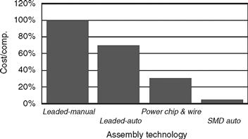
FIGURE 44.4 Relative production costs.
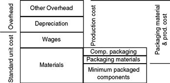
FIGURE 44.5 Full-cost model for circuit partitioning.
The impact of volume on building-block cost applied to three motor drive products is shown in Fig. 44.6. At low volumes, the main savings are in development and maintenance costs, while at high volumes only savings in full cost matters. The overall conclusion is that if a partition is necessary to meet requirements, then, the partition must be guided by strategic choices in order to optimize cost on a company business level and the relative cost diagrams should be used only for optimizing within partitions.
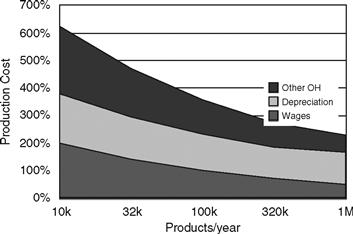
FIGURE 44.6 Cost variation due to volume.
44.6 Technology-driven Partitioning
There are several natural aids to partitioning. Ordering common packaging technologies bytechnical performance, orders most other attributes. As one moves down the list of technologies described in Section 44.4.2, one finds increasing current-carrying capacity, decreasing voltage isolation and operating frequency, lower thermal performance and density, less sophisticated processing, and lower cost for lower volumes (except for MID). These monotonic trends allow rich engineering judgment to effectively group components (step four in Section 44.3.1) for optimized partitioning.
Partitioning proceeds by following a sequence of first grouping and matching the most challenging components with higher performance technologies. The next challenging component grouping is matched with the next technology of lower performance and typically lower cost. Starting with the highest performance technology, often lower performing components to be included at little increase in cost. For example, if thick film ceramic (TFC) is used for chip and wire power die and current-sense resistors, the inclusion of thick-film control circuits comes with little added real estate (cost).
Mixing of technologies and technology selection is misunderstood because a typical perspective is to look at the “substrate area cost,” i.e. the famous “dollars per square inch” costing of technologies. This is as limiting as using only a BOM for cost-driven decisions. A better understanding is required and is aided by the graphical perspective in Fig. 44.7. View the curves right to left as density decreases. The falling curves represent relative Full Cost (Section 44.5) of each technology as substrate area changes. The starting and ending points are the practical limits in the use of the technology at certain densities.
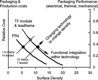
FIGURE 44.7 Cost variation within technologies.
As an example, assume a given circuit is designed with only one technology, such as thick film (TF), and as dense as possible. As the board area increases (becoming less dense), the components grow in size (0603− 0805) with larger interconnect traces; the cost increases, following the curves up and to the left. A point is reached in an area when a less costly technology may be suitable, such as SMT FR-4. This other technology would decrease the cost for the same area. Hence, not only do the cost and density decrease (with lower technology), but the performance also decreases. Within a range near maximum density, the higher performance TF technology with an added area is still less costly. This is due to the packaging and production costs, and is often overlooked by designers who look at the “cost per square area of boards” without looking at the full-cost model.
A more generalized set of curves is shown in Fig. 44.8. This graph, in essence, is created for a specific production facility. The circuit designer, or design team, would follow the steps to partitioning, letting the costs of the technologies drive where partitions are best drawn. Remember that the overall circuitis composed of electric, magnetic, mechanical, and thermal circuits.
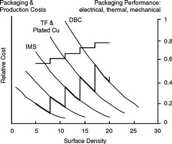
FIGURE 44.8 Generalized relationship of cost and technology.
44.7 Example 2.2 kW Motor Drive Design
A 2.2 kW motor drive, consisting of electronics, motor and pump encased in one housing, is used as an example product. The block diagram of the electronics is shown in Fig. 44.1. For a (planar) electrical-mesh circuit, the physical assembly pattern would closely follow the electrical schematic layout and one packaging technology, such as FR-4, could be used, though not efficiently. The design would, then follow a single line up and to the left in Fig. 44.7. Using mixed packaging technologies provide multiple assembly levels, and the assembly pattern more closely follows grouping of the physical Delivery Forms of the components. The steps outlined in Section 44.3.2 are followed to determine the proper partitioning of the system to meet the performance requirements and provide maximum business profit. The steps are summarized as:
44.7.1 User Requirements (Constraints)
Many user requirements direct the system design as outlined in Section 44.3.1. However, several requirements place specific constraints on the packaging of the 2.2 kW drive as noted below.
| Mechanical: | Built in a 65 mm dia. stainless steel tube; short as possible. |
| Thermal: | Cooling through tube with non-flow of water at 30 C. |
| Environment: | Potting electronics is disallowed. |
| Regulatory: | UL, CE. |
| Reliability: | 1,000,000 quick start/stop, 30,000 maximum gradient start/stop, 40,000 h lifetime @ 10 C water. |
44.7.2 Component Characterization Map
A component characterization map is performed on all the components to identify the technical and physical attributes that dominate it, and is illustrated for part of the circuit as in Table 44.1. In this component characterization map, components are listed for each electrical functional block.
44.7.3 Component Grouping
An overview of possible groupings into packaging partitions is obtained by attaching main components and key attributes to the functional block diagram of Fig. 44.1.
44.7.4 Strategic Partitioning with Constraints
A major constraint is the limited space available (65-mm diameter). This makes it obvious that some miniaturization is very valuable, but what should be miniaturized? Packaging cannot miniaturize leaded components. These components require either through-hole PCB (FR-4, for soldering) or some form of lead frame (MID for welding). Power die are top candidates for miniaturization because the die can be grouped into a power module that is much smaller than discrete power components. Also, high-power losses do not allow the same packaging technologies to be used as for leaded components.
The remaining non-power die and associated components are prime candidates for modularization. Highest value is reached if a building block can be reused across different products. Therefore, as much control circuitry, as possible, should be integrated without violating the possibility for reuse in other products. For this product, the line communications bus and motor control circuitry would be excluded, but the control for VDE/inrush and PFC would be integrated together with the driver and all-sense resistors. This integrates 82% of all power losses for easier cooling, integrates all power-component-dependent control circuitry, and enables product-independent maintenance and power die optimization.
At this stage, there are usually new requirements added for cross-product reuse. This application requires 125°C baseplate temperature.
44.7.5 Optimization within Partitions
Optimization requires choosing optimum technologies to meet cost and performance requirements. In Fig. 44.9, the relative cost of various substrates is shown together with the cost of suitable production technologies. Note that the substrate cost is for equal substrate area but different performance. For example, IMS requires more space for control circuitry than TF multilayer because IMS has only one conductor layer.
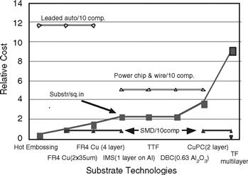
FIGURE 44.9 Substrate costs (1999).
Figure 44.9 should be used together with Fig. 44.1, which shows that the module includes both power chip and wire (PC&W), and low-power control circuitry (SMT). The DBC, IMS, TTF, and CuPC can accommodate the PC&W and FR-4, IMS, TF multilayer, and CuPC can accommodate fine-line SMT. This should initially lead to the conclusion that DBC, IMS, or TTF should be used for power, excluding CuPC due to cost; and FR-4 for control, excluding the others due to cost.
Are all cost issues taken into account and all requirements met? Not necessarily. Packaging approaches influences component cost. Power sense resistors, which are typically in SMT form, can be integrated in TF multilayer at near-zero incremental cost. Also, less-expensive integrated circuits can be chosen when the packaging approach allows active trimming of associated components. Besides cost, technical issues limit packaging choices for certain circuit partitions. Reliability and temperature requirement (125°C) rule out FR-4.
There are fewer and fewer choices. If power die were available as known good die, then power and control could be combined on one substrate with IMS or CuPC. The IMS has drawbacks, such as lower power cycling capability due to a high thermal coefficient of expansion (CTE) and is only a one-layer technology, which means more area and less noise immunity. The CuPC has neither of these problems, but due to the lack of known good power die that was not chosen. Also, CuPC does not allow component integration at the cost indicated in Fig. 44.9. A two-substrate solution was needed.
The power DBC was chosen as the obvious highest performing technology among the comparable low cost power substrates. The DBC is soldered onto a low cost copper base for thermal management and extends to form a mounting base for the control substrate.
Multilayer thick film was chosen for control circuitry despite the apparently high substrate cost. In the motor module, this substrate is the optimum cost choice because of the high component integration, such as the three buried power current-sense resistors and many printed resistors for accurate active trimming of functions associated with the integrated circuits. Partitioning cost is minimized by combining interconnections of substrates with interconnection to I/O terminals in one technology − heavy wire bonding. This has been possible by designing a MID interconnection component with terminals that are wire bondable on one end and solderable on the other. The resulting module is shown in Fig. 44.10.
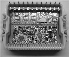
FIGURE 44.10 Final module combining several packaging approaches.
Other components, both SMT and leaded, not best accommodated in the module. Therefore, a two layer FR-4 is chosen as the lowest cost technology suitable for both Delivery Forms and used for the module and components. Mechanical stability and cooling is achieved by using a patented structure of extruded aluminum profiles.
Using bare die, higher cost substrates and partitioning with different technologies allows the product to surpass cost targets. The partitioning in packaging Levels 1 and 2 address optimization of product business cost as defined in Section 44.5. Designing the module building block as a component for reuse across other products increases volume and reduces cost. More importantly, relative low-volume products can benefit from the building block by faster development cycles, lower development cost, lower Level-3 packaging cost, and lower maintenance cost. The building block value addresses optimization of company business cost.
44.8 High Temperature (HT) Packaging [6]
Enabling issues for many power electronics applications are size, weight, and efficiency. Silicon carbide (SiC) semiconductor technology has the potential to provide up to a 5-fold reduction in converter volume if the high-temperature, high-frequency power electronics can be implemented. Higher frequency operation reduces the size of the passive components and, thus, the system volume. Higher operating temperatures allow a larger temperature difference between the heat sink and cooling fluid, which increases radiator effectiveness and decreases size. Silicon devices are limited to 150°C junction temperature prior to de-rating; whereas SiC devices can operate in excess of 400°C. In addition, SiC devices offer the potential for incorporating power electronics at point-of-load (POL), e.g. at the motor or actuator housing, thus greatly reducing system cabling and volume, and provide increased flexibility in equipment arrangement. Inherent in all this is the requirement for very reliable HT electronics packaging.
44.8.1 HT Materials Selection
A paramount requirement of HT packaging is to minimize dissimilarity in material interfaces and can be achieved with a “nearly all” Al (aluminum) approach. This includes Al backed SiC JFETs, A1N substrate, Al2O3 (anodized) electrical insulators, Al interconnects (in place of copper), and AlSiC (aluminum silicon carbide) heat sinks [7]. Aluminum is adequately ductile to act as an excellent stress relief during temperature cycling. Also, Al provides a common metallurgical bonding medium.
44.8.2 Module Construction
A proposed module structure consists of Al conductors on AlN substrate on AlSiC. In a one- to two-step casting process, an Al conductor pattern is formed on AlN, which is captured into a netshape-cast AlSiC heat sink. A test sample was created first with multiple pads for JFETs and wirebonds, shown in Fig. 44.11 (Courtesy of PCC-AFT Inc.). Also, using AlSiC for the housing and heat sink allows a ceramic substrate, connectors, and other hardware to be integrated into the mold, or directly cast into the structure. Connectors that require solder are nickel and gold plated. Other parts of the module follow below.
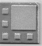
FIGURE 44.11 Al/AIN/AISiC casting.
Aluminum Interconnect − Material properties are given in Table 44.3. Electrical resistance of Al is 2.5 × higher than Cu and 40% lower in thermal conductance. The performance reduction is offset with the thicker conductor greatly mitigating stresses between the components. Both Al and Cu approximately double the resistance every 100°C.
TABLE 44.3 Material properties
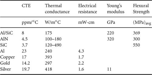
Die Attachment − A significant challenge is die attach. The SiC semiconductor must be bonded to the Al interconnect with a material electrically conductive, having a high physical resistance to temperature excursion, and imparting little stress on substrate or die during power and temperature cycling. One approach uses a silver-glass composite, which can be cured and operate at or above 350°C. One material (QMI3555R) has electrical conductivity of 15 μΩ-cm and thermal conductivity 80W/m-K, and is qualified replacement for Si/Au Eutectic.
Cover Coating and Sealing − If required, an inert HT cover coating, such as an alumina refractory cement (Cotronics 920), can be used across die and wire bonds. The material has the properties of alumina ceramic, devoid of outgassing, completely inert, and good to a service temperature of up to 1634°C. The coefficient of thermal expansion (CTE) is 4.5 ppm/°C, dielectric strength 270V/mil, and volume resistivity 1011W-cm.
Acknowledgment
The author wish to thank Mr. John B. Jacobsen, Technical Manager, Electronic Engineering and Packaging Department of Grundfos A/S, Denmark, for supplying most of the application data used in the module design.
About the Author
Dr. Hopkins received BS and MS degrees from the State University of New York at Buffalo (UB), and Ph.D. from Virginia Tech (VPI&SU) where his primary study was in megahertz-frequency power supplies using high-density packaging techniques. He is an Associate Research Professor, Director of the Electronic Power and Energy Research Laboratory, Assistant Director of the Electronic Packaging Laboratory at UB, and and IEEE and IMAPS senior member. He chairs the power electronics packaging technical committees for IEEE-CPMT, IEEE-PELS, and IMAPS. He has authored over 50 journal and conference publications. He also has over 15 years of industrial experience at GEs and Carrier Air Conditioning Companys’ R&D centers, was visiting fellow at several national labs and is president of DCHopkins & Associates.
Further Reading
1. Meinhardt M, Cheasty P, Eckert S, Flannery J, ÓMathúna SC, Alderman A. STATPEP-Current Status of Power Electronics Packaging for Power Supplies - Methodology. Proc. of the 14th Annual Applied Power Electronics Conference and Exposition. March 14–18, 1999; 16–22.
2. Hopkins DC, ÓMathúna SC, Alderman A, Flannery J. A Framework for Developing Power Electronics Packaging. Proc. of the 14th Annual Applied Power Electronics Conference and Exposition. February 15–19, 1998; 9–15.
3. Tummala RR, Rymaszewski EJ. Microelectronics Packaging Handbook. New York: Van Nostrand Reinhold; 1989.
4. High Voltage Integrated Circuits. In: Baliga BJ, ed. New York: IEEE Press; 1988. [IEEE order number: PC0232-9].
5. Jacobsen JB, Hopkins DC. Optimally Selecting Packaging Technologies and Circuit Partitions based on Cost and Performance. Applied Power Electronics Conference. February 6–10, 2000.
6. Hopkins DC, Kellerman DW, Wunderlich RA, Basaran C, Gomez J. High-Temperature, High-Density Packaging of a 60 kW Converter for > 200°C Embedded Operation. IEEE Applied Power Electronics Conference. March 19–24, 2006.
7. Hopkins DC, Pitarressi JM, Karker JA. “Systems Design Considerations for Using a Direct-Attached-Ceramic MMC Power Package,” PCIM ’96 EUROPE. Proc. 32nd Int’l Power Conversion Conf.. 1996; 683–689 [Nurnberg, Germany].