Chapter 13. Extending Functionality
Kramer: It’s just a write-off for them.Jerry: How is it a write-off?Kramer: They just write it off.Jerry: Write it off what?Kramer: Jerry, all these big companies, they write-off everything.Jerry: You don’t even know what a write-off is.Kramer: Do you?Jerry: No. I don’t.Kramer: But they do and they are the ones writing it off.
In this chapter, we introduce additional hardware and software technologies that you may encounter in embedded systems. We begin with a look at a pair of chip interconnection buses called I2C and SPI. Next we introduce programmable logic, including FPGAs. And finally, we take a look at adding a TCP/IP network.
Common Peripherals
As you work on more and more embedded systems, you will come across different peripherals that you will have to use. In this section, we take a look at some of the common embedded peripherals that you will likely encounter. Sometimes it is necessary to implement these protocols entirely in software (see the sidebar “Serial Bit Banging” later in this chapter).
Serial buses can be either asynchronous or synchronous. In an asynchronous serial connection, the data is sent without using a common timing clock signal. To align the receiver with the sender, there is some sort of start condition to signify when the transmission begins, and a stop condition to indicate the end of transmission. A synchronous serial connection typically uses a separate clock signal to synchronize the receiver with the sender. Synchronous connections may also use a start and stop condition to synchronize the receiver and sender, after which the sender must send characters one right after the other.
A serial interface that can send and receive data at the same time is called full-duplex. A serial interface that must alternate between sending and receiving data is called half-duplex.
Inter-Integrated Circuit Bus
One of the common serial buses used in embedded systems is the Inter-Integrated Circuit bus, commonly referred to as the I 2 C (pronounced “eye squared see”) bus. This bus is common in embedded systems because it doesn’t require much in the way of hardware resources and is ideal for low-speed, short-distance communications. The I2C bus, created by Philips, is a two-wire (data and clock) communication system. I2C includes the addressing of individual devices (up to 127 in Standard-mode, 1024 in extended mode) to allow multiple devices on the same bus.
Various maximum data rates are supported by different revisions to the I2C specification. These data rates are up to 100 Kbps for Standard-mode, 400 Kbps for Fast-mode, and 3.4 Mbps for High-speed mode. Devices of different data rates can be mixed on the same bus. The I2C specification can be found online at http://www.semiconductors.philips.com.
The PXA255 processor includes an I2C bus interface unit. Additional information about this can be found in the PXA255 Processor Developer’s Manual.
Some devices that typically contain I2C bus interfaces are EEPROMs and real-time clock chips. Figure 13-1 shows an example I2C bus with multiple devices.

The two I2C bus signals are serial data (SDA) and serial clock (SCL). The master on the bus initiates all transfers; other devices on the bus are called slaves. In Figure 13-1, the microprocessor is the master and the other devices are the slaves. Both master and slaves can receive and transmit data on the bus.
The master initiates transactions on the bus and controls the clock signal. Because of this, a slave device needs a way of holding off the master during a transaction. When a slave holds off the master device to perform flow control on the incoming data, it is called clock stretching. During this time the slave keeps the clock line pulled low until it is ready to continue with the transaction. It is important that all master devices support this feature. Figure 13-2 is the format of an I2C bus transaction. All data on the bus is communicated most significant bit first (MSB).
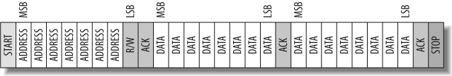
An I2C bus data transaction begins by the master initiating a start condition. A start condition occurs when the master causes a high-to-low transition on the data line while the clock line is held high.
Next, the 7-bit unique address of the device is sent out by the master device. Each device on the bus checks this address with its own to determine whether the master is communicating with it. I2C slave devices come with a predefined device address. The lower bits of this address are sometimes configurable in hardware.
Then the master outputs the read or write bit. If the bit is high, the transaction is a read, where data goes from the slave to the master device. If the bit is low, the transaction is a write from the master to the slave device.
The slave device then sends an acknowledge bit. For the acknowledge bit, the data line is kept low while the clock signal is high. Acknowledge bits always are sent by the slave device.
Now, depending on the type of transaction (read or write), the transmitter (which can be slave or master) begins sending a byte of data, starting with the MSB. At the end of the data byte, the receiver (either slave or master) issues an acknowledge bit. This pattern is continued until all of the data has been transferred.
The transaction ends with the master device causing a stop condition. A stop condition occurs when the master causes a low-to-high transition on the data line while holding the clock line high. Note that the I2C protocol supports multiple masters.
Serial Peripheral Interface
Another serial bus that is commonly used in embedded systems is the Motorola serial peripheral interface (SPI, pronounced “spy”). Another similar serial interface is Microwire, trademarked by National Semiconductor, which is a restricted subset of SPI.
SPI can operate at data rates up to 1 Mbps. It can additionally operate in full-duplex mode, making it better suited than I2C for applications where data is constantly flowing. I2C uses fewer signals than SPI, can communicate over several feet (a meter or more), and has a well defined specification. SPI, on the other hand, has a limited communication length of a few inches. SPI does not support multiple masters or specify a device addressing scheme; therefore, additional hardware signals are needed in order to select specific slaves. This lack of addressing can be a benefit because it reduces the overhead in single-master, single-slave SPI interfaces.
Figure 13-3 shows an example of an SPI bus structure. In this figure, there is a single master and two slave devices connected to the SPI bus.
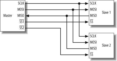
The SPI bus includes 3 + N signals, where N is the number of slaves on the bus. In Figure 13-3, there are two slaves, so the SPI bus requires five signals. These signals are serial clock (SCLK), data signal Master Out Slave In (MOSI), data signal Master In Slave Out (MISO), and Slave Select (SS1 and SS2). The slave select signal is used to select which slave the master wants to communicate with. In this example, because there are two slave devices, two slave select signals are needed. This shows how additional hardware resources are needed in the SPI interface to accommodate the lack of addressing in the protocol.
SPI operates in full-duplex mode. During communications, the master device initiates a transaction by generating a clock and selecting a device using the slave select signal. Data is then transferred in both directions on the MOSI and MISO lines. Because data is transferred in both directions, it is up to each device to know whether the incoming data is meaningful—that is, whether the transaction was a read, write, or both.
Another difference between SPI and I2C is that SPI does not include any type of acknowledgment mechanism. The transmitter has no way of knowing data has been received at the destination. There is also no mechanism for flow control included in SPI. If flow control is needed, it must be implemented outside of SPI.
Programmable Logic
Programmable logic chips are widely used in embedded systems. These devices allow hardware engineers to perform various tasks (such as chip select logic) in hardware. As a programmer, you might not design the logic within the programmable device, but you may need to write a driver to download the program into an FPGA.
This section will give you a better basis for communicating with hardware designers to determine which functions should be implemented in dedicated logic, programmable logic, and/or software. We’ve found that there are valid reasons for choosing each of these three implementation techniques. You must pay close attention to the requirements of the particular application to make the correct decision.
Many types of programmable logic are available. The current range of offerings includes everything from small devices capable of implementing only a handful of logic equations to huge devices that can hold an entire processor core (plus peripherals!). In addition to this incredible difference in size, architectures also vary greatly. We’ll introduce you to the most common types of programmable logic and highlight the most important features of each type.
Programmable Logic Device
At the low end of the spectrum is the original Programmable Logic Device (PLD). PLDs were the first chips that could be used to implement a flexible digital logic design in hardware. In the early days, you could remove a couple of the 7400-series Transistor-Transistor-Logic (TTL) parts (ANDs, ORs, and NOTs) from your board and replace them with a single PLD. Other names you might encounter for this class of device are Programmable Logic Array (PLA), Programmable Array Logic (PAL), and Generic Array Logic (GAL).
PLDs are often used for address decoding, where they have several clear advantages over the 7400-series TTL parts that they replaced. Firstly, one chip typically requires less board area and wiring. Another advantage is that the design inside the chip is flexible, so a change in the logic doesn’t require any rewiring of the board. Rather, the decoding logic can be altered by simply replacing the single, previously installed PLD with another part that has been programmed with the new Boolean logic.
Inside each PLD is a set of connected macrocells. These macrocells are typically comprised of some amount of combinatorial logic (AND and OR gates, for example) and a flip-flop. In other words, a small Boolean logic equation can be built within each macrocell. This equation combines the state of some number of binary inputs into a binary output and, if necessary, stores that output in the flip-flop until the next clock edge. Of course, the particulars of the available logic gates and flip-flops are specific to each manufacturer and product family. But the general idea is always the same.
Hardware designs for these simple PLDs are generally written in languages such as ABEL or PALASM (the hardware equivalents of assembly language) or drawn with the help of a schematic capture tool.
Complex Programmable Logic Device
As chip densities increased, it was natural for the PLD manufacturers to evolve their products into larger parts (logically, but not necessarily physically) called Complex Programmable Logic Devices (CPLDs). For most practical purposes, CPLDs can be thought of as multiple PLDs (plus some programmable interconnect) in a single chip. The larger capacity of a CPLD allows you to implement either more logic equations or a more complicated design. In fact, these chips are large enough to replace dozens of those pesky 7400-series parts.
Figure 13-4 contains a block diagram of a hypothetical CPLD. Each of the four logic blocks shown is equivalent to one PLD. However, in an actual CPLD there may be more (or fewer) than four logic blocks. Figure 13-6 is a simplified version. The switch matrix allows signal routing and communication between the logic blocks. Note also that these logic blocks are themselves comprised of macrocells and interconnect wiring, just like an ordinary PLD.
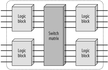
Because CPLDs can hold larger designs than PLDs, their potential uses are more varied. They are still sometimes used for simple applications such as address decoding, but more often contain high-performance control logic or finite state machines. At the high end (in terms of numbers of gates), there is also a lot of overlap in potential applications with FPGAs. Because of its less flexible internal architecture, the delay through a CPLD (measured in nanoseconds) is more predictable and usually shorter.
Field Programmable Gate Array
A Field Programmable Gate Array (FPGA) can be used to implement just about any hardware design. One use is to prototype a lump of hardware that will eventually find its way into an ASIC. However, there is nothing to say that the FPGA can’t remain in the final product, and it quite often does. Whether it does will depend on the relative weights of the development cost and production cost for a particular project, as well as the need to upgrade the hardware design after the product ships. (It costs significantly more to develop an ASIC, but the cost per chip will be lower if you produce them in sufficient quantities. The cost tradeoff involves the expected number of chips to be produced and the expected likelihood of hardware bugs and/or changes. This makes for a rather complicated cost analysis.)
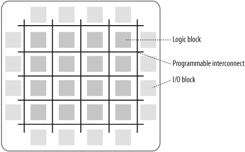
The historical development of the technology in an FPGA was distinct from the PLD/CPLD evolution just described. This is apparent when you look at the structures inside. Figure 13-5 illustrates a typical FPGA architecture. There are three key parts to its structure: logic blocks, interconnect, and I/O blocks. The I/O blocks form a ring around the outer edge of the part. Each of these provides individually selectable input, output, or bi-directional access to one of the GPIO pins on the exterior of the FPGA package. Inside the ring of I/O blocks lies a rectangular array of logic blocks. And finally, connecting logic blocks to logic blocks and I/O blocks to logic blocks, the programmable interconnect wiring runs through the array.
The logic blocks within an FPGA can be as small and simple as the macrocells in a PLD (a so-called fine-grained architecture) or larger and more complex (a coarse-grained architecture). However, the logic blocks in an FPGA are never as large as an entire PLD, as are the logic blocks of a CPLD. Remember that the logic blocks of a CPLD contain multiple macrocells. But the logic blocks in an FPGA are generally nothing more than a couple of logic gates or a look-up table and a flip-flop.
Because of all the extra flip-flops, the architecture of an FPGA is much more flexible than that of a CPLD. This makes FPGAs better in register-heavy and pipelined applications. They are also often used in place of a processor-plus-software solution, particularly where the processing of input data streams must be performed at a very fast pace. In addition, FPGAs are usually denser (more gates in a given area) than their CPLD cousins, so they are the de facto choice for larger logic designs.
Pulse Width Modulation
Pulse width modulation (PWM) is a powerful technique for controlling analog circuits with a processor’s digital outputs. PWM is employed in a wide variety of applications, ranging from measurement and communications to power control and conversion.
Analog circuits
An analog signal has a continuously varying value, with effectively infinite resolution in both time and magnitude. A 9 V battery is an example of an analog device, in that its output voltage is not precisely 9 V, but changes over time and can take any real value from 0.0 V to about 9.5 V. Similarly, the amount of current drawn from a battery is not limited to a finite set of possible values. Analog signals are distinguishable from digital signals because the latter always take values only from a finite set of predetermined possibilities, such as the set of two values (0 V, 5 V).
Analog voltages and currents can be used to control things directly, such as the volume of a car radio. In a simple analog radio, a knob is connected to a variable resistor. As you turn the knob, the resistance goes up or down. As that happens, the current flowing through the resistor increases or decreases. This might directly change the amount of voltage driving the speakers, thus increasing or decreasing the volume.
As intuitive and simple as analog control may seem, it is not always economically attractive or otherwise practical. For one thing, analog circuits tend to drift over time and can, therefore, be very difficult to tune. Precision analog circuits, which solve that problem, can be very large, heavy (just think of old home stereo equipment), and expensive. Analog circuits can also get very hot; the power dissipated is proportional to the voltage across the active elements multiplied by the current through them. Analog circuitry can also be sensitive to noise. Because of its infinite resolution, any perturbation or noise on an analog signal necessarily changes the current value.
Digital control
Controlling analog circuits digitally can drastically reduce system costs and power consumption. What’s more, many microcontrollers and DSPs already include on-chip PWM controllers, making implementation easy.
In a nutshell, PWM is a way of digitally encoding analog signal levels. Through the use of high-resolution counters, the duty cycle (the percentage of time that a signal is asserted) of a square wave is modulated to encode a specific analog signal level. The PWM signal is still digital because, at any given instant, the full DC supply is either fully on or fully off. The voltage or current source is supplied to the analog load by means of a repeating series of on and off pulses. The on-time is the time during which the DC supply is applied to the load, and the off-time is the period during which that supply is switched off. Given a sufficiently small period of the PWM signal, any analog value can be encoded with PWM.
To help explain the relation between digital encoding and analog values, we show three different PWM signals in Figure 13-6. Figure 13-6(a) shows a PWM output at a 10 percent duty cycle. That is, the signal is on for 10 percent of the period and off for the other 90 percent. Figures 13-6(b) and 13-6(c) show PWM outputs at 50 percent and 90 percent duty cycles, respectively. These three PWM outputs encode three different analog signal values, at 10 percent, 50 percent, and 90 percent of the full strength. If, for example, the supply is 9 V and the duty cycle is 10 percent, a 0.9 V analog signal results.

In Figure 13-7, we show a simple circuit that could be driven using PWM. In this figure, a 9 V battery powers an incandescent lightbulb. If the switch connecting the battery and lamp is closed for 50 ms, the bulb receives the full 9 V during that interval. If we then open the switch for the next 50 ms, the bulb receives 0 V. If we repeat this cycle 10 times a second, the bulb will be lit as though it were connected to a 4.5 V battery (50 percent of 9 V). We say that the duty cycle is 50 percent and the modulating frequency is 10 Hz. (Note that we’re not advocating you actually power a lightbulb this way; we just think this an easy-to-understand example.)

Most loads require a much higher modulating frequency than 10 Hz. Imagine that our lamp was switched on for five seconds, then off for five seconds, then on again. The duty cycle would still be 50 percent, but the bulb would appear brightly lit for the first five seconds and not lit at all for the next. In order for the bulb to see a voltage of 4.5 V, the cycle period must be short relative to the load’s response time to a change in the switch state. To achieve the desired effect of a dimmer (but always lit) lamp, it is necessary to increase the modulating frequency. The same is true in other applications of PWM. Common modulating frequencies range from 1 to 200 kHz.
One of the advantages of PWM is that the signal remains digital all the way from the processor to the controlled system; no digital-to-analog conversion is necessary. Keeping the signal digital minimizes noise effects. Noise can affect a digital signal only if the noise is strong enough to change a logical 1 to a logical 0, or vice versa.
This increased noise immunity is another benefit of choosing PWM over analog control and is the principal reason PWM is sometimes used for communications. Switching from an analog signal to PWM can increase the length of a communications channel dramatically. At the receiving end, a suitable resistor-capacitor (RC) or inductor-capacitor (LC) network can remove the modulating high-frequency square wave and return the signal to analog form.
PWM finds application in a variety of systems. As a concrete example, consider a PWM-controlled brake. To put it simply, a brake is a device that clamps down hard on something. In many brakes, the amount of clamping pressure (or stopping power) is controlled with an analog input signal. The more voltage or current that’s applied to the brake, the more pressure the brake will exert.
The output of a PWM controller could be connected to a switch between the supply and the brake. To produce more stopping power, the software need only increase the duty cycle of the PWM output. If a specific amount of braking pressure is desired, measurements would need to be taken to determine the mathematical relationship between duty cycle and pressure. (And the resulting formulae or lookup tables would be tweaked for operating temperature, surface wear, and so on.)
To set the pressure on the brake to, say, 100 psi, the software would do a reverse lookup to determine the duty cycle that should produce that amount of force. It would then set the PWM duty cycle to the new value and the brake would respond accordingly. If a sensor is available in the system, the duty cycle can be tweaked, under closed-loop control, until the desired pressure is precisely achieved.
Networking for All Devices Great and Small
Incorporating networking support in an embedded device might seem like a daunting task at first glance. However, even an older embedded system can be updated with a software network stack to extend its feature set and incorporate modern conveniences such as emailing an administrator when alarms occur, and a web server to provide a remote user interface accessible from any web browser.
Certainly, there are costs to including a network stack. The network interface (such as Ethernet) can quickly become expensive and complicated. You may need extra hardware (with additional costs for chips and connectors, board space, and power consumption) and software (with new drivers). However, this does not have to be the case. You could run a simple Serial Line Interface Protocol (SLIP) or Point to Point Protocol (PPP) over a UART port for the network interface. Most embedded processors include at least one UART, and SLIP and PPP are very basic protocols to implement—no more difficult than the Monitor and Control program we looked at in Chapter 9.
The demands of a network stack may cause you to worry that too many system resources are required. The processing power and memory needed to accommodate network support can be greatly reduced by choosing the proper network stack. Several software network stacks that are targeted at embedded systems, where processor cycles and memory are limited, are currently available in the open source community.
The next section is intended to give you an overview of some of the benefits of adding networking support and includes some options of resource-conscious networking stacks that are ideal for incorporation into embedded systems.
Benefits of Network Support
Adding networking support, Transmission Control Protocol/Internet Protocol (TCP/IP) and the other supporting protocols grouped in this suite enable standardized access to a device. TCP/IP enables a device to communicate using the native protocol of most networking infrastructures, which allows the device to be accessed from a PC, PDA, or web-enabled cellular phone. The network-enabled device can communicate over a Local Area Network (LAN) or through the global Internet.
For additional information about networking protocols, take a look at the three-volume series TCP/IP Illustrated, by Richard Stevens (Addison-Wesley). Another resource is TCP/IP Guide: A Comprehensive, Illustrated Internet Protocols Reference, by Charles Kozierok (No Starch Press).
Each device can be tailored to use the ideal protocol to transmit information over the network. The very low-overhead User Datagram Protocol (UDP) can be used for data not requiring acknowledgment, whereas TCP is available for data that needs confirmation of its receipt from the destination.
Networking support can improve the basic feature set that an embedded device is capable of supporting. For example, if an alarm condition occurs in the system, the device can generate an email and send it off to notify the network operator of the error. The network operator can then quickly perform the necessary maintenance to correct the problem and get the system back to normal—keeping the system downtime to a minimum.
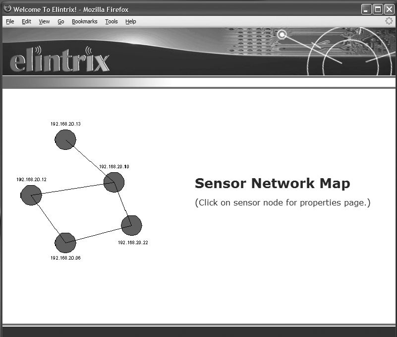
Another benefit of networking is that web-based management can be easily incorporated into the device. Web-based management allows configuration and control of a system using TCP/IP protocols and a web browser. A technician can connect directly to a device for configuration and monitoring using a standard PDA equipped with a standard web browser. The device’s web server and HyperText Markup Language (HTML) pages are the new user interface for the device. Many devices today, such as cable modem routers and firewalls, include a web interface for configuration. Figure 13-8 shows the interface to a network of sensor devices presented by a web server that enables web-based management.
Networking Solutions for Embedded Systems
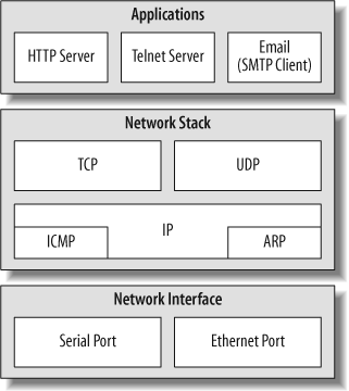
There are several commercial and open source network stack solutions available today. Most stacks offer standard protocol suites, and some include example applications to help you extend your device’s basic feature set. Figure 13-9 shows some of the common network protocol components included with most networking stacks. We’ll list even more protocols later in this chapter as we describe particular networking solutions.
One of the keys in deciding which stack will best fit your device is to determine the resource requirements the software needs in order to operate. The amount of data the device transmits and receives during communication sequences should also dictate which solution is right for your design. For example, if your device is a sensor node that wakes up every hour to transmit a few bytes of data, a compact network stack implementation is ideal. In contrast, a video monitoring system that is constantly transmitting large amounts of data might need a stack implementation that offers better packet buffer management.
Implementations focused on small embedded devices allow networking to be integrated into even the most resource-constrained system. It is important that the “lightweight” network stack implementation you choose allows communication with standard, full-scale TCP/IP devices. An implementation that is specialized for a particular device and network might cause problems by limiting your ability to extend the device’s network capabilities in other, generic networks.
It is always possible to go off and roll your own network stack. However, given the wide range of solutions available in the open source community, leveraging existing technology is usually the better choice and enables you to quickly move your development forward.
In the following list of software network stacks, we focus on open source solutions that are ideal for resource-constrained embedded devices. This list is not intended to be comprehensive, but rather a starting point for further investigation. All of the networking stacks listed include TCP/IP protocol support. A brief description of each network stack is included; for more detailed information, refer to the specific web pages listed. (BSD networking code is something of an industry standard and therefore appears as the basis of many of the projects listed.)
- lwIP (http://savannah.nongnu.org/projects/lwip)
This “ lightweight IP” stack is a simplified but full-scale TCP/IP implementation. lwIP was designed to be run in a multithreaded system with applications executing in concurrent threads, but it can also be implemented on a system with no operating system. In addition to the standard TCP/IP protocol support, lwIP also includes Internet Control Message Protocol (ICMP), Dynamic Host Configuration Protocol (DHCP), Address Resolution Protocol (ARP), and UDP. It supports multiple local network interfaces. lwIP has a flexible configuration that allows it to be easily used in a wide variety of devices and scaled to fit different resource requirements.
- OpenTCP (http://www.opentcp.org)
Tailored to 8- and 16-bit microcontrollers, OpenTCP incorporates the ICMP, DHCP, Bootstrap Protocol (BOOTP), ARP, and UDP. This package also includes several applications, such as a Trivial File Transfer Protocol (TFTP) server, a Post Office Protocol Version 3 (POP3) client to retrieve email, Simple Mail Transfer Protocol (SMTP) support to send email, and a Hypertext Transfer Protocol (HTTP) server for web-based device management.
- TinyTCP (http://www.unusualresearch.com/tinytcp/tinytcp.htm)
This network stack is designed to be very modular and to include only the software required by the system. For example, different protocols can be included based on your configuration. TinyTCP provides a BSD-compatible socket library and includes the ARP, ICMP, UDP, DHCP, BOOTP, and Internet Group Management Protocol (IGMP).
- uC/IP (http://ucip.sourceforge.net)
uC/IP (pronounced mew-kip)[1] is designed for microcontrollers and based on BSD network software. Protocol support includes ICMP and Point-to-Point Protocol (PPP).
- uIP (http://www.sics.se/~adam/uip)
This “micro IP” stack is designed to incorporate only the minimal set of components necessary for a full TCP/IP stack solution. There is support for only a single network interface. Application examples included with uIP are SMTP for sending email, a Telnet server and client, an HTTP server and web client, and Domain Name System (DNS) resolution.
Each network stack has been ported to various processors and microcontrollers. The device driver support for the network interface varies from stack to stack. It is a good idea to review the license for the network stack you decide to use, to make sure it does not place undesirable limitations or requirements on your product.
In addition, some operating systems include or have network stacks ported to them. The operating systems covered earlier in this book, eCos and embedded Linux (see Chapters 11 and 12), both offer networking support modules. eCos includes the OpenBSD, FreeBSD, and lwIP network stacks as well as application-layer support for many of the extended features discussed previously. Embedded Linux, having been developed for a desktop PC environment, offers extensive network support.
If a network stack is included or already exists in your device, several embedded web servers are available to incorporate web-based control. One such open source solution is the GoAhead WebServer (http://www.goahead.com).
Embedding a networking stack is no longer a daunting task that requires an enormous amount of resources. The solutions listed previously can quickly be leveraged and integrated to bring networking features to any embedded system. Tailoring one of the network stack solutions to the specific characteristics of a device ensures that the system will operate at its optimal level and best utilize system resources.