
5Space vector pulse width modulation for multilevel inverters using fractal approach
In this chapter, the space vector pulse width modulation (SVPWM) for multilevel inverters using fractal approach has been proposed and implemented for three-and five-level inverters. This method is mainly based on the fact that the switching vector representation of any multilevel inverter has an inherent fractal structure, which is the basic unit of this structure, being a triangle made of the vertices of three adjacent inverter voltage space vectors. The proposed method uses simple arithmetic for determining the sector and does not require look-up tables; hence, the fractal approach is applied for multilevel inverters using SVPWM. The results have been presented and analyzed. The complexity and feasibility of this algorithm have been discussed.
The space vector representation of a higher-level inverter can be conceived as generated from the space vector representation of the two-level inverter, wherein the sectors of the two-level inverter get progressively divided and subdivided. The basic structure, a triangle (sector), is transformed by further dividing itself into smaller triangles. A basic structure that evolves by dividing itself into structures similar to it has an associated fractal. The switching voltage space vector representation of multilevel inverters also has an associated fractal. In fractal theory, the basic triangle is divided into four smaller triangular regions, joined by the midpoints of the sides of the triangle [101].
5.1Inherent fractal structure of multilevel inverter
The voltage space vectors of the two-level inverter are shown in Fig. 5.1. The voltage space vector locations for a three-level inverter are shown in Fig. 5.2, where A00, A01, A02, A03, A04, A05, and A06 are same as the locations of the voltage space vectors of the two-level inverter. Consider the region marked 1 in the case of the two-level inverter, formed by the vectors located at A00, A01, and A02. In the case of the three-level inverter, this region has three additional voltage space vectors, as shown in Fig. 5.2.
It can be observed that the three additional voltage space vectors are located at the midpoints of each side of the sector of equivalent two-level inverter. The three additional switching voltage space vectors together with switching voltage space vectors located at A00, A01, and A02 results in four sectors within (sector 1) A00, A01, A02 of the three-level inverter. Considering the triangular region formed by the space vectors located at A00, A01, and A02, besides the voltage space vectors of the three-level inverter, nine additional voltage space vectors are present, as shown in Fig. 5.3. The nine additional vectors are located at A21, A22, A23, A24, A25, A26, A27 , A28, and A29. It can be clearly observed that the nine additional vectors are located at the midpoints of the sides of sectors of the three-level inverter. The nine additional vectors together with the voltage space vectors of the three-level inverter results in 16 sectors within (sector І) ΔA00A01A02 of the five-level inverter. In this manner each sector in the voltage space vector representation of an equivalent two-level inverter is divided into four smaller sectors, resulting in voltage space vector locations of the three-level inverter. Each of the sectors of the three-level inverter is further divided into four smaller sectors resulting in switching space vectors of the five-level inverter. This process gets repeated for generation of space vectors of higher-level inverters.

Fig. 5.1: Voltage space vectors of the two-level inverter.

Fig. 5.2: Voltage space vectors of the three-level inverter.

Fig. 5.3: Voltage space vectors of the five-level inverter by inherent fractal structure.
5.2SVPWM algorithm using the fractal approach
This algorithm explains the procedure to adopt the SVPWM for multilevel inverters using the fractal approach.
i.Three-phase (a, b, c) to two-phase (d, q) transformation.
ii.Identify the sector where the tip of the reference vector is located.
iii.Determine the three nearest voltage vectors.
iv.Perform the triangularization algorithm.
v.Calculate and compare the centroids of each triangle with the reference vector.
vi.For the higher-level implementation of the fractal approach, perform the triangularization algorithm until the reference vector is nearer to the centroids of respective triangle where the triangularization is to be performed using Eqs. (5.12) to (5.14).
vii.Switching states are obtained using Eqs. (5.15) to (5.17).
viii.Switching time durations are calculated, taking the basic two-level timings into consideration.
ix.Optimized switching sequence is calculated by (a) taking the virtual zero vectors, (b) eliminating the redundant switching states, and (c) considering optimum switching where only one switching is involved as the inverter changes from one state to another.
5.2.1Three-phase (a, b, c) to two-phase (d, q) transformation
The three phase quantities can be transformed to their equivalent two phase quantities either in synchronously rotating frame or stationary frame. From this two-phase component the reference vector magnitude can be found and used for modulating the inverter output.
The three phase sinusoidal voltage components are
The magnitude and angle of the rotating vector can be found by means of Clark’s transformation. Then, the (d, q) coordinates of the corresponding space vector can be obtained as
5.2.2Location of the reference voltage vector
The identification of sector where the tip of the reference vector lies can be done using coordinate transformation of the reference vector into a two dimensional coordinate system. The sector can also be determined by resolving the reference phase vector along a, b and c axes and by repeated comparison with discrete phase voltages.

Fig. 5.4: Location of the reference vector in the two-level inverter.
After identifying the sector, the voltage vectors at the vertices of the sector are to be determined. This can be done by the comparison of reference angle with sector angle; Fig. 5.4 depicts SVPWM with six sectors in (d, q) reference frame with α as the reference angle.
If the reference angle
The location of tip of reference frame passing through different layers can be found in Fig. 5.5. If the reference vector is in layer 1, it represents the two-level inverter operation and the reference vector in layer 2 represents the three-level inverter, the reference vector in layer 3 represents the four-level inverter, and the reference vector in layer 4 represents the five-level inverter.
After identifying the sector, the voltage vectors at the vertices of the sector are to be determined. The nearest three voltage vectors of the reference vector are the vertices of the sector.
5.2.3Determination of nearest three voltage vectors
The space vector voltage is located in a hexagon surrounded by different states of the inverter that gives different voltage magnitudes of the output voltage. These inverter states are nothing but the ON/ OFF states of the devices. After identifying the sector where the tip of the reference vector is located, the voltage vectors of this sector are determined to find out the three nearest voltage vectors of space vector voltage Vsr. To obtain these three nearest voltage vectors, the region where the space vector voltage lies should be determined.

Fig. 5.5: Locus of the tip of the reference vector passing through different layers of the five-level inverter.
If the reference vector lies in sector 1, the three nearest vectors are determined by the comparison of the reference angle. If reference angle α < 60°, it lies in the first sector, and hence, three nearest voltage vectors are V0, V1, and V 2. For example, if the reference angle lies in sector 4, the nearest three vectors are V0, V4, V5 or V4, V5, V7.
5.2.4Triangularization algorithm
As explained earlier, due to the inherent fractal structure associated with multilevel inverter, the voltage space vector representation of the two-level inverter grows to that of higher-level inverters by repeated division of each sector. At every stage, the triangular region is divided into four smaller triangular regions, due to the presence of the additional voltage vectors as shown in Fig. 5.6. The three additional voltage vectors are located at the midpoint of each side of sector. The sectors of higher-level inverter can therefore be generated by such repeated triangularization.

Fig. 5.6: Triangularization of the two-level inverter in sector I.
The following steps are involved to perform the triangularization
i.Determine the sector where the triangularization is to be performed.
ii.Determine the midpoints of each side of the sector using Eqs. (5.12) to (5.14). These are the coordinates of the three new vectors that will divide the sector into four smaller, but similar, triangular regions.
iii.Determine the inverter states corresponding to these vectors using Eqs. (5.15) to (5.17).
For example, consider region I of the two-level inverter formed by vertices A00, A01, and A02. The coordinates of three vertices are (α00, β00), (α01, β01), and (α02, β02), respectively. The coordinates of the three new voltage space vectors located at A11, A12, and A13 as shown in Fig. 5.7 can be obtained from the coordinates of A00, A01, and A02.
Coordinates of A11 are
Coordinates of A12 are

Fig. 5.7: Sector I of the two-level inverter.

Fig. 5.8: First triangularization of the two-level inverter.
The associated switching vector states can also be determined in a similar manner. The inverter switching states corresponding to the voltage space vector located at A00, A01, and A02 are (a0 b0 c0), (a1 b1 c1), and (a2 b2 c2), respectively. The switching states of the new voltage space vectors as shown in Fig. 5.8 at A11 (a3 b3 c3), A12 (a4 b4 c4), and A13 (a5 b5 c5) can be obtained as
where X takes a, b, and c for the respective phases.
Eqs. (5.12) to (5.14) represent the arithmetic procedure used in the proposed method for dividing a triangular region (sector) into four similar regions by generating three additional vectors situated at the midpoints of the sides forming the original triangular region. This is referred as the triangularization algorithm. To generate sectors of higher-level inverter by progressively dividing sectors of the two-level inverter, the triangularization algorithm is repeatedly applied. In fractal theory, algorithms whose repeated iterations will result in the pattern to grow or evolve are referred as iterated function system, the repeated iteration of triangularization algorithm will grow the inherent fractal structure in space vector representation of multilevel inverters. Therefore, the triangularization algorithm can be viewed as the iterated function system for this fractal structure.
5.2.5Comparison of the reference vector with the centroid
The location of the tip of the reference voltage space vector from among these four triangular regions is found by determining the region whose centroid is closest to the tip of the reference space vector. The coordinates of the centroid of an equilateral triangle can be determined as the average of coordinates of the three vertices. For an equilateral triangle with the coordinates of the vertices as (α1, β1), (α2, β2), (α3, β3), the coordinates of the centroid (αcent, βcent) is given by
The triangle with the centroid closest to the tip of the reference space vector is ΔA11, A12 AI3. The triangularization algorithm has to be applied again in case of the five-level inverter. The application of Eqs. (5.12) to (5.14) to ΔA11A12A13 will generate further three new voltage space vectors A23, A25, A26 and also the inverter states corresponding to these new voltage vectors. Thus, the three-level inverter space vector diagram is further divided into four smaller triangles for a five-level inverter space vector diagram, as shown in Fig. 5.9.

Fig. 5.9: Triangularization of sector I of equivalent three-level inverter.
From these four triangles, one triangle enclosing the reference space vector is chosen such that its centroid is closest to the tip of the reference space vector. The sector is identified and the inverter states corresponding to the switching vectors located at the vertices of the identified sector are also generated simultaneously.
5.2.6Calculation of switching times
The switching time durations are calculated, taking the basic two-level timings into consideration, as these can be extended to the N-level. The switching voltage vectors approximate the volt-second of the reference space vector by operating for specific durations. The determination of duration of operation of the switching voltage space vectors is simplified by mapping the sector that is identified to enclose the reference space vector to a sector of the two-level inverter.
The switching time durations of the vectors can be determined using the following formulae from Eqs. (5.19) to (5.22).
where
According to the magnitude of the voltage vectors, they are divided into four groups: zero-voltage vectors (ZVV), small-voltage vectors (SVVs), middle-voltage vectors (MVV), and large-voltage vectors (LVV). Both ZVVs and SVVs have redundant switching states. The mapping is done by choosing one of the three vectors of the identified sector to coincide with the actual zero vectors in the voltage space vector representation of the inverter. In the present work, the vector selected to coincide with the actual zero vector is referred to as the virtual zero vector. The vector with the minimum value for the sum of the magnitudes of the α and β coordinates is chosen to be the virtual zero vector for a particular sector. The sum of the magnitudes of the α and β coordinates represents the total offset of the vector from the actual zero vector. Therefore, in the present work, the virtual zero vectors chosen are at minimum offset from the zero vectors.
5.3Algorithm implementation for the three-level inverter
This section explains the proposed method for generation of SVPWM for the three-level inverter using the inherent fractal structure associated with the switching space vector representation of multilevel inverter.
5.3.1Determination of switching vectors
The process of obtaining the reference space vector includes the transformation of (a, b, c) to (d, q) coordinates. Sector identification determines the triangle that encloses the tip of the reference space vector. The vertices of the triangle represent the locations of switching voltage space vectors used to synthesize the reference space vector.
The (d, q) components of the space vector of an N-level inverter can be normalized through division by Vdc/N – 1, where Vdc is the dc-link voltage. In the case of a three-level inverter, the voltage Vdc, in the normalized space vector representation is therefore represented by a vector of length 2 as shown in Fig. 5.10.
For a three-level inverter, the switching vectors located at the six vertices of the hexagon forming the periphery are same as the vectors of equivalent two-level inverter, but they have the switching states as (200), (220), (020), (022), (002), (202).
The position of the reference space vector A00P for a three-level inverter is as shown in Fig. 5.11. The first step in the proposed sector identification method is to determine the location of the tip of the reference space vector A00P from among the six regions of the equivalent two-level inverter. This step is implemented by the comparison of the instantaneous reference phase voltages. In this case, the reference space vector A00P is located in region I of the equivalent two-level inverter. Region I is formed by the vertices A00, A01, and A02. The coordinates of the vertices are (0,0), (2,0), and (1,1.732), respectively. The switching states corresponding to the vectors located at A00, A01, and A02 are also shown in Fig. 5.11(a). The switching states of the vector located at A00, A01, and A02 are (000, 111, 222), (200), and (220), respectively. The next step is to divide region I into four smaller triangular regions by applying the triangularization algorithm, which will generate the coordinates of the new voltage space vectors and the inverter states corresponding to these new switching vectors. The three new voltage space vectors divide region I into four smaller triangular regions marked R1, R2, R3, and R4 as shown in Fig. 5.11(b). Thus, by determining the switching states through triangularization algorithm for the three-level inverter, 27 switching states and sectors are represented in Fig. 5.12.

Fig. 5.10: Space vector representation of the three-level inverter.

Fig. 5.11: Sector identification and switching vector determination of the three-level inverter.

Fig. 5.12: Switching states and sectors of the three-level inverter.
5.3.2Determination of centroid
The location of the tip of the reference voltage space vector A00P among these four triangular regions is found by determining the region whose centroid is closest to the tip of the reference space vector. The coordinates of the centroid of an equilateral triangle can be determined as the average of coordinates of the three vertices. For an equilateral triangle with the coordinates of the vertices as (α1, β1), (α2, β2), (α3, β3), the coordinates of the centroid (αcent, βcent) can be obtained from Eq. (5.18).
The triangle with the centroid closest to the tip of the reference space vector is ΔA11A12A13. From among these four triangles, the triangle enclosing the reference space vector A00P is ΔA11A12A13, as its centroid is closest to the tip of the reference space vector. The ΔA11, A12, A13 corresponds to sector 8. The sector is identified and the inverter states corresponding to the switching vectors located at the vertices of the identified sector are also generated simultaneously.
5.3.3Determination of switching times
The voltage reference vector A00P is identified in sector 8 as shown in Fig. 5.29(b). The voltage space vector with the tip located at A12 becomes the virtual zero vector for sector 8. Sector 8 thus gets mapped to sector 1 of the three-level inverter. The determination of duration now reduces to that of a two-level inverter, since after mapping, one of the vectors of the identified sector coincides with the zero vectors. The durations of the vectors can be determined as in the case of the two-level inverter.
5.3.4Determination of optimized switching sequence
Once the switching vectors are determined and their respective durations are calculated, the vectors are to be switched in an optimum sequence such that only one switching occurs when the inverter changes its state. In the SVPWM technique, optimum switching is achieved using the redundant states of the zero vector for alternate switching cycles. In this chapter, optimum switching is achieved using two redundant switching states of the respective virtual zero vector in the alternate cycles. The tip of the reference vector A00P is located in sector 8. The switching states corresponding to the switching vectors at the vertices of sector 8 with redundancies are A11 (100,211), A12 (110,221), and A13 (210). For sector 8, the virtual zero vector at A12 has two redundant switching states whereas the voltage vectors at A11 has two redundancies and A13 has one redundancy. If the redundancy of the virtual zero vector is greater than two, the last two redundant switching states are selected for the virtual zero vector. For the other two vectors, if redundant states are more than one, the last redundant state is selected. In case of the three-level inverter, as the zero vector at A12 has two redundant switching states, both of these are selected. As the space vector A11 has more than one redundant state, the last switching state is selected. As A13 has only one redundant state, it is selected. This strategy of choosing the last two redundant states for the virtual zero vector and the last redundant state for the other vectors will achieve optimum switching sequence. The selection will result in switching states 110-210-211-221 for the virtual zero vector. With this switching sequence, only one switching occurs as the inverter changes its state.

Fig. 5.13: Space vector diagram of the three-level inverter with rotating reference vector.
By following the above procedure of the fractal approach for the three-level inverter, the switching states and switching sequence of a reference vector is generated. Considering twelve samples of the reference vector in a single sector, as shown in Fig. 5.13, by rotating reference angle from 0° to 360°, a total of 72 samples are obtained. The optimized switching sequence for 72 samples is determined and presented in Tab. 5.1.
Tab. 5.1: Switching states of the three-level inverter.
5.4Implementation of the algorithm for the five-level inverter
This section explains the proposed method for generation of SVPWM for the five-level inverter using the inherent fractal structure associated with the switching space vector representation of multilevel inverter. The schematic diagram of the five-level inverter is shown in Fig. 5.14.
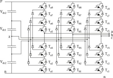
Fig. 5.14: Five-level diode-clamped inverter.
The dc bus voltage is split into five levels using four dc capacitors, C1, C2, C3, and C4. Each capacitor has Vdc/4 V each voltage stress will be limited to one capacitor level through clamping diodes. In the five-level inverter, clamping diodes clamped the bus voltage into three voltage levels, +Vdc/2, +Vdc/4, 0, –Vdc/4, –Vdc/2. These states are defined as 4, 3, 2, 1, and 0, respectively. There are N3 possible states, i.e. 125 states for the five-level inverter and it consists of (5 – 1) = 4 capacitors on the dc bus, 2(5 – 1) = 8 switching devices per phase and 2(5 – 2) = 6 clamping diodes per phase.
5.4.1Determination of switching vectors
In the case of the five-level inverter, voltage Vdc, in the normalized space vector representation, is represented by a vector of length 4. The switching vectors located at the six vertices of the hexagon forming the periphery are the same as the vectors of the equivalent two-level inverter, but they have switching states (400), (440), (040), (044), (004), (404).
The position of the reference space vector A00P for the five-level inverter is as shown in Fig. 5.15. The switching states of five-level inverter are shown in Fig. 5.16. The first step in the proposed sector identification of this method is to determine the location of the tip of the reference space vector A00P from among the six regions of the equivalent two-level inverter. Region I is formed by the vertices A00, A01, and A02. The coordinates of the vertices are (0,0), (4,0), and (2, 2√3), respectively, as shown in Fig. 5.17. The switching states of the vector located at A00, A01, and A02 are (000, 111, 222, 333, 444), (400), and (440), respectively. The next step is to divide region I into four smaller triangular regions by applying the triangularization algorithm and generates the coordinates of the new voltage space vectors and the inverter states corresponding to these new switching vectors. The three new voltage space vectors divide region I into four smaller triangular regions marked as R1, R2, R3, and R4 as shown in Fig. 5.17.

Fig. 5.15: Space vector representation of the five-level inverter.
5.4.2Determination of centroids
The location of the tip of the reference voltage space vector A00P among these four triangular regions is found by determining the region whose centroid is closest to the tip of the reference space vector. The coordinates of the centroid of an equilateral triangle can be determined as the average of coordinates of the three vertices.
The triangle with the centroid closest to the tip of the reference space vector is ΔA11A12AI3 for the five-level inverter, the triangularization algorithm has to be applied again, which generates further three new voltage space vectors and the inverter states corresponding to these new voltage vectors, thus dividing it into four smaller triangles, with ΔA23A25A26 as the triangle enclosing the reference space vector A00P, as its centroid is closest to the tip of the reference space vector. The ΔA23A25A26 corresponds to sector 27 of the five-level inverter. The sector is identified and the inverter states corresponding to the switching vectors located at the vertices of the identified sector are also generated simultaneously.

Fig. 5.16: Switching states of the five-level inverter.
5.4.3Determination of switching times
For the voltage reference vector A00P, the sector identified is sector 27. The voltage space vector with tip located at A23 becomes the virtual zero vector for sector 27. Sector 27 thus gets mapped to sector 1 of the five-level inverter. The determination of duration now reduces to that of a two-level inverter since after mapping one of the vectors of the identified sector coincides with the zero vectors. The durations of the vectors can be determined using the conventional two-level inverter.
5.4.4Determination of optimized switching sequence
The tip of the reference vector A00P is located in sector 27, as shown in Fig. 5.17. The switching states corresponding to the switching vectors at the vertices of sector 27 with redundancies are A23 (210, 321, 432), A25 (310, 421) and A26 (320, 431). For sector 27, the virtual zero vector at A23 has three redundant switching states while the voltage vectors at A25 and A26 has two redundancies each. In the present work, if the redundancy of the virtual zero vector is greater than two, the last two redundant switching states are selected for the virtual zero vector. For the other two vectors, if redundant states are more than one, the last redundant state is selected. This strategy of choosing the last two redundant states for the virtual zero vector and the last redundant state for the other vectors will achieve optimum switching sequence. The selection will result in switching states 321–432 for the virtual zero vector. The other vectors have switching states 421 and 431. With these states, the switching sequence of inverter for sector 27 is 321–421–431–432 during a sampling interval and 432–431–421–321 for the subsequent sampling interval. Note that only one switching occurs as the inverter changes state.

Fig. 5.17: Sector identification and switching vector determination of the five-level inverter.
By following the above procedure of the fractal approach for the five-level inverter, the switching states and switching sequence of a reference vector are generated. Considering twelve samples of the reference vector in a single sector, as shown in Fig. 5.18 by rotating the reference angle from 0° to 360°, 72 samples are obtained. The optimum switching pattern for these 72 samples obtained through implementation of fractal approach for the five-level inverter is shown in Tab. 5.2.

Fig. 5.18: Space vector diagram of the five-level inverter with rotating reference vector.
To validate the proposed method of the generation of SVPWM for multilevel inverters using the fractal approach, simulation studies have been carried out with a dc-link voltage of 400 V and modulation index of 0.8. The simulation parameters used in this method are given in Appendix II. Figures 5.19 and 5.20 show the simulation results for the three-level inverter. Figures 5.19 and 5.20 show the process of triangularization and rotation of the reference voltage vector of the three-level inverter, respectively. Figure 5.19 shows the basic SVPWM where the first triangularization was done to locate the reference voltage vector. Figure 5.20 shows the rotation of the reference voltage vector through 0° to 360° in the d-q reference frame. From Fig. 5.20, it is clear that the reference vector is rotated from 0° to 360°, and by the proposed technique, the sectors are clearly identified, when the tip of the reference vector moved from sector 7 to sector 24. As the reference vector is changing from one sector to another, the simultaneous switching sequence is given to the multilevel inverter.
Tab. 5.2: Switching states of the five-level inverter.
| Samples | States | Switching states |
| 1 | 66-102-103-67 | 300-400-410-411 |
| 2 | 67-103-69-66 | 411-410-310-300 |
| 3 | 68-103-67-69 | 310-410-411-421 |
| 4 | 69-104-103-68 | 421-420-410-310 |
| 5 | 68-103-104-69 | 310-410-420-421 |
| 6 | 71-69-104-70 | 431-421-420-320 |
| 7 | 70-104-105-71 | 320-420-430-431 |
| 8 | 71-105-73-70 | 431-430-330-320 |
| 9 | 72-105-71-73 | 330-30-431-441 |
| 10 | 73-106-105-72 | 441-440-430-330 |
| 11 | 72-105-106-73 | 330-430-440-441 |
| 12 | 73-106-105-72 | 441-440-430-330 |
| 13 | 72-107-106-73 | 330-340-440-441 |
| 14 | 73-106-107-72 | 441-440-340-330 |
| 15 | 72-107-75-73 | 330-340-341-441 |
| 16 | 75-107-108-74 | 341-430-240-230 |
| 17 | 74-108-107-75 | 230-240-340-341 |
| 18 | 75-77-108-74 | 341-241-240-230 |
| 19 | 76-109-108-77 | 130-140-240-241 |
| 20 | 77-108-109-76 | 241-240-140-130 |
| 21 | 76-109-79-77 | 130-140-141-241 |
| 22 | 79-109-110-78 | 141-140-040-030 |
| 23 | 49-111-110-78 | 030-040-140-141 |
| 24 | 79-109-110-78 | 141-140-040-030 |
| 25 | 78-110-111-79 | 030-040-041-141 |
| 26 | 79-111-110-78 | 141-041-040-030 |
| 27 | 80-111-79-81 | 031-041-141-142 |
| 28 | 81-112-111-80 | 142-042-041-031 |
| 29 | 80-111-112-81 | 031-041-042-142 |
| 30 | 83-81-112-82 | 143-142-042-032 |
| 31 | 82-112-113-83 | 032-042-043-143 |
| 32 | 83-113-112-82 | 143-043-042-032 |
| 33 | 84-113-83-85 | 033-043-143-144 |
| 34 | 85-114-113-84 | 144-044-043-033 |
| 35 | 84-113-114-85 | 033-043-044-144 |
| 36 | 85-114-113-84 | 144-044-043-033 |
| 37 | 84-115-114-85 | 033-034-044-144 |
| 38 | 85-114-115-84 | 144-044-034-033 |
| 39 | 84-115-87-85 | 033-034-134-144 |
| 40 | 87-115-116-86 | 134-034-024-023 |
| 41 | 86-116-115-87 | 023-024-034-134 |
| 42 | 87-89-116-86 | 134-124-024-023 |
| 43 | 88-117-116-89 | 013-014-024-124 |
| 44 | 89-116-117-88 | 124-024-014-013 |
| 45 | 88-117-91-89 | 013-014-114-124 |
| 46 | 91-117-118-90 | 114-014-004-003 |
| 47 | 90-118-117-91 | 003-004-014-114 |
| 48 | 91-117-118-90 | 114-014-004-003 |
| 49 | 90-118-119-91 | 003-004-104-114 |
| 50 | 91-119-118-90 | 114-104-004-003 |
| 51 | 92-119-91-93 | 103-104-114-214 |
| 52 | 93-120-119-92 | 214-204-104-103 |
| 53 | 92-119-120-93 | 103-104-204-214 |
| 54 | 95-93-120-94 | 314-214-204-203 |
| 55 | 94-120-121-95 | 203-204-304-314 |
| 56 | 95-121-120-94 | 314-304-204-203 |
| 57 | 96-121-95-97 | 303-304-314-414 |
| 58 | 97-120-121-96 | 414-404-304-303 |
| 59 | 96-121-120-97 | 303-304-404-414 |
| 60 | 97-120-121-96 | 414-404-304-303 |
| 61 | 96-123-122-97 | 303-403-404-414 |
| 62 | 97-122-123-96 | 414-404-403-303 |
| 63 | 96-123-99-97 | 303-403-413-414 |
| 64 | 99-123-124-98 | 413-403-402-302 |
| 65 | 98-125-123-99 | 302-402-403-413 |
| 66 | 99-101-124-98 | 413-412-402-302 |
| 67 | 100-125-124-100 | 301-401-402-412 |
| 68 | 101-124-125-100 | 412-402-401-301 |
| 69 | 100-125-67-101 | 301-401-411-412 |
| 70 | 67-125-102-66 | 411-401-400-300 |
| 71 | 66-102-125-67 | 300-400-401-411 |
| 72 | 67-125-102-66 | 411-401-400-300 |
Figs. 5.21 and 5.22 show the pole voltages and line voltages of the three-level inverter, respectively. Figures 5.23 and 5.24 show the phase voltages and gate currents, respectively. Figure 5.25 shows the stator currents of the three-level inverter fed induction motor. The rotor speed and torque of the three-level inverter fed induction motor are shown in Figs. 5.26 and 5.27, respectively. The harmonic spectrum of the inverter output voltage and the total harmonic distortion (THD) are shown in Fig. 5.28.

Fig. 5.19: Space vector diagram of the three-level inverter for a basic reference angle (α) of 6°.
Figs. 5.28 to 5.38 show the simulation results for the five-level inverter. Figures 5.28 and 5.29 show the process of triangularization and rotation of the reference voltage vector of the five-level inverter, respectively. Figure 5.28 shows the basic SVPWM where the triangularization was done to locate the reference voltage vector. Figure 5.29 shows the rotation of the reference voltage vector through 0° to 360° through sectors 25 to 54 in the d-q reference frame.
Figs. 5.30 and 5.31 show the pole voltages and line voltages of the five-level inverter, respectively. Figures 5.32 and 5.33 show the phase voltages and gate currents, respectively. Figures 5.34 and 5.35 show the stator currents of the five-level inverter fed induction motor, respectively. The rotor speed and torque of the five-level inverter fed induction motor are shown in Figs. 5.36 and 5.37, respectively. The harmonic spectrum of the five-level inverter output voltage and the THD are shown in Fig. 5.38. The comparison between the three- and five-level inverters with the proposed algorithm is given in Tab. 5.3. These results show that the five-level inverter attains a steady-state response faster than the three-level inverter and that the torque ripple and the THD are reduced.

Fig. 5.20: Space vector diagram of the three-level inverter when reference angle (α) rotated through 360°.

Fig. 5.21: Pole voltages of the three-level inverter.

Fig. 5.22: Line-to-line voltages of the three-level inverter.

Fig. 5.23: Phase voltages of the three-level inverter.

Fig. 5.24: Gate currents of the three-level inverter.

Fig. 5.25: Stator currents of the three-level inverter fed induction motor.

Fig. 5.26: Speed response of the three-level inverter fed induction motor.

Fig. 5.27: Torque response of the three-level inverter fed induction motor.

Fig. 5.28: Output line voltage harmonic spectrum of the three-level inverter.

Fig. 5.29: Space vector diagram of the five-level inverter for a basic reference angle (α) of 6°.

Fig. 5.30: Space vector diagram of the five-level inverter when reference angle (α) rotated through 360°.

Fig. 5.31: Pole voltages of the five-level inverter.
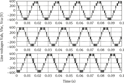
Fig. 5.32: Line-to-line voltages of the five-level inverter.

Fig. 5.33: Phase voltages of the five-level inverter.

Fig. 5.34: Gate currents of the five-level inverter.

Fig. 5.35: Stator currents of the five-level inverter fed induction motor.

Fig. 5.36: Stator current of the five-level inverter fed induction motor.

Fig. 5.37: Speed response of the five-level inverter fed induction motor.

Fig. 5.38: Torque response of the three-level inverter fed induction motor.

Fig. 5.39: Output voltage harmonic spectrum of the five-level inverter.
The results of three- and five-level inverters have been analyzed and shown in Tab. 5.3. The harmonic spectrum of five-level inverter output voltage is as shown in Fig. 5.39. The five-level inverter shows improved performance than the three-level inverter.
Tab. 5.3: Performance of the three- and five-level inverters.

In the field of high-power, high-performance applications, multilevel inverters seem to be the most promising alternative. In this chapter, an algorithm for the generation of SVPWM for multilevel inverter based on fractals has been proposed and applied for three- and five-level inverters. In this method, the switching sequence is determined without using look-up tables, so the memory of the controller can be saved. The switching times of the voltage vectors are calculated at the same manner as two-level SVPWM. Thus, the proposed method reduces the execution time of the three- and five-level SVPWM. The triangularization algorithm is easy to implement, as basic arithmetic is used. It can also be applied to the SVPWM method for N-level. The obtained THDs for the three- and five-level inverters are 5.70% and 3.61%, respectively, which is much less, compared with the conventional SVPWM algorithm.