
6Qualitative space vector pulse width modulation algorithm for multilevel inverters
In this chapter, a qualitative space vector pulse width modulation (SVPWM) algorithm is proposed and implemented for neutral point-clamped (NPC) multilevel inverter. In this method, the duty cycles of the reference voltage vectors are corrected accordingly to identify the location of the reference voltage vector in each region. The appropriate switching sequence of the region and calculation of the switching ON times for each state are estimated. This scheme can be extended to high-level inverters as well. This algorithm has been discussed in detail, and results have been presented and analyzed for two, three, four, five, six and seven-level inverters. The total harmonic distortion (THD) has been calculated, and comparison with lower levels is also presented in this chapter.
The conventional SVPWM algorithm and a novel approach for the generation of SVPWM for multilevel inverters based on fractals are presented in the previous chapters. However, as the number of level increases, the location of the reference voltage vector, optimum switching sequence and dwelling time calculations, and the control algorithm become increasingly complex. To improve the performance of multilevel inverters, a qualitative SVPWM algorithm is proposed and analyzed in this chapter.
6.1A qualitative SVPWM algorithm for multilevel inverters
Sector identification can be done using coordinate transformation of the reference vector into a two-dimensional coordinate system. The sector can also be determined by resolving the reference phase vector along the a, b and c-axes and by repeated comparison with discrete phase voltages. After identifying the sector, the voltage vectors at the vertices of the sector are to be determined. Once the switching voltage space vectors are determined, the switching sequences can be identified using lookup tables. The calculations of the duration of the voltage vectors can be simplified by mapping the identified sector corresponding to a sector of the two-level inverter. To obtain optimum switching, the voltage vectors are to be switched for their respective durations, in a sequence such that only one switching occurs as the inverter moves from one switching state to another [126].
The duty cycles of the reference voltage vector will be m1, m2, and [1 − (m1 + m2)]. The values of m1 and m2 are useful in identifying the region where reference vector is located, which is the major problem in the case of multilevel inverters.
In this method, a correction to the duty cycles of the reference vector is applied to identify the location of the reference vector easily in each region of a multilevel inverter. Once the region is identified, the appropriate switching sequence of the region can be identified. The ON time period for each state can be calculated with the obtained duty cycles.
The circuit diagram and space vector diagram of seven-level NPC inverter are as shown in Figs. 6.1 and 6.2, respectively. In case of the seven-level inverter, six switches from each phase leg will be ON at any time point to produce predetermined output at phases. The possible switching combinations will be 343, with 216 redundant states. SVPWM is quite different from other PWM techniques. With other PWM techniques, the inverter can be thought of as three separate stages, which create each phase wave form separately. However, the SVPWM treats an inverter as a single unit, with each inverter in specific unique state. Modulation is achieved by switching the state of the inverter. The SVPWM is a digital modulating technique whose the objective is to generate PWM load line voltages that are, in average, equal to given (or reference) load line voltages. This is done in each sampling period by properly selecting the switching states of the inverter and calculating the appropriate time period for each state. The SVPWM is an advanced and computation-intensive PWM method.
The space vector (Vsr) constituted by the pole voltages of inverters Vao, Vbo, and Vco with 120° phase displacement can be defined as
The dwelling time periods T1, T2, and T0 are
In multilevel inverters, the reference voltage vector can be reproduced in the average sense by switching among the inverter states situated at the vertices, which are in closest proximity to it. In the case of the two-level inverter, the identification of the reference vector location in a sector is straightforward. However, in a higher-level inverter, the existence of more than one region in the sector will require additional mathematical computation to identify the region where the reference vector is located. The duty cycles (ON time for each state) will be found by equating the volt-seconds of the reference voltage with the nearest three states.

Fig. 6.1: Seven-level NPC inverter topology.
where d1, d2, and d3 are the duty cycles of the nearest voltage vectors V1, V2, and V3 and m is the voltage reference vector.
6.2.1Calculation of duty cycles
The vector states at the vertices of each region can be identified from space vector diagrams. Consider the space vector diagram of sector 1 of the seven-level inverter, shown in Fig. 6.3. The reference vector m3 is located in region 2 of the three-level inverter. m6 and m7 are the reference vectors located in region 21 of the six-level inverter and region 29 of the seven-level inverter, respectively. mx1 and mx2 (x = 3 or 6 or 7) are projections of the reference vectors onto zero axis and 60° axis (angle θ is made by the reference vector from the zero axes, i.e. start sector 1; noted that m3, m6, and m7 have different angle θ values). The reference vector can be synthesized by sequential switching operation of the three nearest switching states (vertices of the region where the reference vector is located).
The lengths of new vectors can be found using

Fig. 6.2: Space vector diagram of the seven-level inverter.
The values of m1 and m2 for the reference vector in each region can be calculated using Eq. (6.6). The duty cycles of the vertices of the reference voltage will be m1, m2, and [1 − (m1 + m2)]. For example, with reference to m3 (reference vector in region 2), the reference vector can be synthesized by switching vectors V1, V2, and V3. It is important to note that the duty cycle for switching state V1 shall be the length of the vector joining V3 and V1, whereas m1 is the projection of reference vector m3 from the origin. As such, the corrected duty cycle for switching state V1 in the present case would be (m1 − 0.167). The length of the vector joining V3 and V2 is m2. As such, the corrected duty cycles for the switching states V1, V2, and V3 would be (m1 − 0.167), m2, and (0.833 − m1 − m2), respectively.
The values of m1 and m2 are useful in identifying the region where the reference vector is located, which is the major problem in multilevel inverters. The conditions for identifying the reference vector location in each region and the corrected duty cycles for each of the level of inverter are shown in Tab 6.1. Once the region is identified, the appropriate switching sequence of a region can be identified.

Fig. 6.3: Sector I of the seven-level inverter.
The ON time period for each state can be calculated with the duty cycles obtained:
6.2.2A qualitative SVPWM algorithm
- Find the sector where Vref lies.
- Calculate m1, m2 from Eq. (6.6) and compute (m1 + m2) of the reference voltage.
- Find the region where Vref is located.
- Identify the nearest three vectors (vertices of region) to the Vref.
- Select appropriate switching sequences.
- Compute ON time for each switching state.
- Place the inverter states in the respective states for the calculated ON times.
The flowchart for the implementation of qualitative space vector pulse width modulation algorithm for multilevel inverters is as shown in Fig. 6.4.

Fig. 6.4: Flowchart of qualitative SVPWM for multilevel inverter.
6.2.4Location of the reference vector and correction of duty cycles
The conditions for identifying reference vector location in seven-level inverter and the corrections required for the duty cycles are indicated in Tab. 6.1. The switching ON and OFF sequences are as shown in Tab. 6.2.
Tab. 6.1: Location of the reference vector and corrected duty cycles.
| Region | Condition for location of the reference vector | Corrected m 1, m 2, and m 3 for the switching states |
| 26 | 0.834 < m1 < 1 | m1 = m1 − 0.833 |
| m2 < 0.167 | m2 = m2 | |
| (m1 + m2) < 1 | m3 = 1 − m1 − m2 | |
| 27 | 0.667 < m1 < 0.834 | m1 = 0.833 − m1 |
| m2 < 0.167 | m2 = 0.167 − m2 | |
| (m1 + m2) > 0.834 | m3 = m1 + m2 − 0.834 | |
| 28 | 0.667 < m1 < 0.834 | m1 = m1 − 0.667 |
| 0.167 < m2 < 0.333 | m2 = m2 − 0.167 | |
| (m1 + m2) < 1 | m3 = 1 − m1 − m2 | |
| 29 | 0.5 < m1 < 0.667 | m1 = 0.667 − m1 |
| 0.167 < m2 < 0.333 | m2 = 0.333 − m2 | |
| (m1 + m2) > 0.834 | m3 = m1 + m2 − 0.834 | |
| 30 | 0.5 < m1 < 0.667 | m1 = m1 − 0.5 |
| 0.333 < m2 < 0.5 | m2 = m2 − 0.333 | |
| (m1 + m2) < 1 | m3 = 1 − m1 − m2 | |
| 31 | 0.333 < m1 < 0.5 | m1 = 0.5 − m1 |
| 0.333 < m2 < 0.5 | m2 = 0.5 − m2 | |
| (m1 + m2) > 0.834 | m3 = m1 + m2 − 0.834 | |
| 32 | 0.333 < m1 < 0.5 | m1 = m1 − 0.333 |
| 0.5 < m2 < 0.667 | m2 = m2 − 0.5 | |
| (m1 + m2) < 1 | m3 = 1 − m1 − m2 | |
| 33 | 0.167 < m1 < 0.333 | m1 = 0.5 − m1 |
| 0.5 < m2 < 0.667 | m2 = 0.667 − m2 | |
| (m1 + m2) > 0.834 | m3 = m1 + m2 − 0.834 | |
| 34 | 0.167 < m1 < 0.333 | m1 = m1 − 0.167 |
| 0.667 < m2 < 0.834 | m2 = m2 − 0.667 | |
| (m1 + m2) < 1 | m3 = 1 − m1 − m2 | |
| 35 | m1 < 0.167 | m1 = 0.167 − m1 |
| 0.667 < m2 < 0.834 | m2 = 0.834 − m2 | |
| (m1 + m2) > 0.834 | m3 = m1 + m2 − 0.834 | |
| 36 | m1 < 0.167 | m1 = m1 |
| 0.834 < m2 < 1 | m2 = m2 − 0.834 | |
| (m1 + m2) < 1 | m3 = 1 − m1 − m2 |
Tab. 6.2: Switching sequence of the seven-level inverter.


To validate the proposed qualitative SVPWM algorithm for multilevel inverters, the simulation studies have been carried out for two, three, four, five, six and seven-level inverters. The simulation parameters and specifications of the induction motor used in this method are given in Appendix III. The results for the two-level inverter are shown in Figs. 6.5 to 6.10. The phase voltages and line voltages of the two-level inverter are shown in Figs. 6.5 and 6.6, respectively. The output voltage harmonic spectrum and the THD are shown in Fig. 6.7. The stator currents, rotor speed, and torque of the two-level inverter fed induction motor are shown in Figs. 6.8 to 6.10, respectively. The results for the three-level inverter are shown in Figs. 6.11 to 6.16. The phase and line voltages are shown in Figs. 6.11 and 6.12, respectively.
The harmonic spectrum of the output voltage and the THD are shown in Fig. 6.13. The stator currents, rotor speed, and torque of the three-level inverter fed induction motor are shown in Figs. 6.14 to 6.16, respectively. The results of the four-level inverter are shown in Figs. 6.17 to 6.22. The phase voltages, line voltages, output voltage harmonic spectrum, and THD are shown in Figs. 6.17 to 6.19, respectively. The stator currents, rotor speed, and torque of the four-level inverter fed induction motor are shown in Figs. 6.20 to 6.22, respectively. The results of the five-level inverter are shown in Figs. 6.23 to 6.28. The phase voltages, line voltages, output voltage harmonic spectrum, and THD are shown in Figs. 6.23 to 6.25, respectively. The stator currents, rotor speed, and torque of the four-level inverter fed induction motor are shown in Figs. 6.26 to 6.28, respectively. The results of the six-level inverter are shown in Figs. 6.29 to 6.34. The phase voltages, line voltages, output voltage harmonic spectrum, and THD are shown in Figs. 6.29 to 6.31, respectively.
The stator currents, rotor speed, and torque of the four-level inverter fed induction motor are shown in Figs. 6.32 to 6.34, respectively. The results of the seven-level inverter are shown in Figs. 6.35 to 6.40. The phase voltages, line voltages, output voltage harmonic spectrum, and THD are shown in Figs. 6.35 to 6.37, respectively. The stator currents, rotor speed, and torque of the four-level inverter fed induction motor are shown in Figs. 6.38 to 6.40, respectively. From these results, it is observed that as the level of the inverter is increased, the THD is decreased, as shown in Tab. 6.3. and torque ripples are also greatly reduced.

Fig. 6.5: Phase voltages of the two-level inverter.

Fig. 6.6: Line-to-line voltages of the two-level inverter.

Fig. 6.7: Output line voltage (and its harmonic spectrum) of the two-level inverter.

Fig. 6.8: Stator currents of the two-level inverter fed induction motor.

Fig. 6.9: Speed response of the two-level inverter fed induction motor.

Fig. 6.10: Torque response of the two-level inverter fed induction motor.

Fig. 6.11: Phase voltages of the three-level inverter.

Fig. 6.12: Line-to-voltages of the three-level inverter.

Fig. 6.13: Output line voltage (and its harmonic spectrum) of the three-level inverter.

Fig. 6.14: Stator currents of the three-level inverter fed induction motor.

Fig. 6.15: Speed response of the three-level inverter fed induction motor.

Fig. 6.16: Torque response of the three-level inverter fed induction motor.
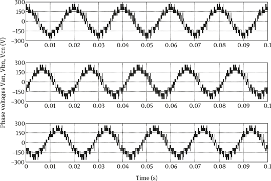
Fig. 6.17: Phase voltages of the four-level inverter.

Fig. 6.18: Line-to-line voltages of the four-level inverter.
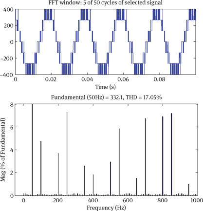
Fig. 6.19: Output line voltage (and its harmonic spectrum) of the four-level inverter.

Fig. 6.20: Stator currents of the four-level inverter fed induction motor.

Fig. 6.21: Speed response of the four-level inverter fed induction motor.

Fig. 6.22: Torque response of the four-level inverter fed induction motor.

Fig. 6.23: Phase voltages of the five-level inverter.

Fig. 6.24: Line-to-line voltages of the five-level inverter.

Fig. 6.25: Output line voltage (and its harmonic spectrum) of the five-level inverter.

Fig. 6.26: Stator currents of the five-level inverter fed induction motor.

Fig. 6.27: Speed response of the five-level inverter fed induction motor.

Fig. 6.28: Torque response of the five-level inverter fed induction motor.
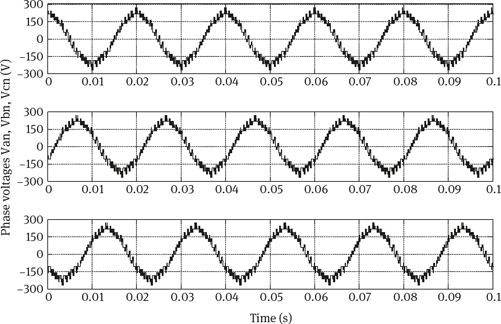
Fig. 6.29: Phase voltages of the six-level inverter.

Fig. 6.30: Line-to-line voltages of the six-level inverter.

Fig. 6.31: Output line voltage and its harmonic spectrum) of the six-level inverter.

Fig. 6.32: Stator currents of the six-level inverter fed induction motor.

Fig. 6.33: Speed response of the six-level inverter fed induction motor.

Fig. 6.34: Torque response of the six-level inverter fed induction motor.

Fig. 6.35: Phase voltages of the seven-level inverter.

Fig. 6.36: Line-to-line voltages of the seven-level inverter.

Fig. 6.37: Output line voltage (and its harmonic spectrum) of the seven-level inverter.

Fig. 6.38: Stator currents of the seven-level inverter fed induction motor.

Fig. 6.39: Speed response of the seven-level inverter fed induction motor.

Fig. 6.40: Torque response of the seven-level inverter fed induction motor.
Tab. 6.3: THD of multilevel inverters.
| Inverter | THD (%) |
| Two-level inverter | 42.48 |
| Three-level inverter | 24.99 |
| Four-level inverter | 17.05 |
| Five-level inverter | 11.57 |
| Six-level inverter | 6.71 |
| Seven-level inverter | 4.67 |
In this chapter, a qualitative SVPWM algorithm has been proposed and described for the three, four, five, six and seven-level inverters. In this proposed scheme, the duty cycles of the reference voltage vectors are corrected to identify the location of the reference voltage vector easily in each region. The appropriate switching sequence of the region and dwelling time calculation are also proposed. The results have been presented and analyzed, which show that the generated voltage spectrum is very much improved with the increase in the level of inverter. The THD is highly reduced as the level of inverter increases. The input current drawn by the induction motor is less distorted as the level of inverter increases. The output voltage THD for the three-, four-, five-, six-, and seven-level inverters is 42.48%, 24.99%, 17.05%, 11.57%, 6.71%, and 4.67%, respectively, which is considerably lower than that of the same inverter using the other modulation techniques.