
7Space vector pulse width modulation for multilevel inverters using the decomposition method
In this chapter, the space vector pulse width modulation (SVPWM) algorithm for multilevel inverters using the decomposition method is presented. In this method, the space vector diagram of the multilevel inverter is decomposed into several space vector diagrams of the two-level inverters. The SVPWM algorithm using the decomposition method is applied for the seven-level inverter. In this method, the space vector diagram of the seven-level inverter is decomposed into six space vector diagrams of the four-level inverters. In turn, each of these six space vector diagrams of the four-level inverter is decomposed into six space vector diagrams of the three-level inverters, and each of these six space vector diagrams of the three-level inverter is decomposed into six space vector diagrams of the two-level inverters. To proceed with the switching state determination, first, one of these hexagons is selected based on the location of the target voltage vector. Second, the original voltage reference vector is decremented by the voltage vector that locates the origin of the selected two-level hexagon. This then allows the determination of switching sequence and calculation of the voltage vector duration to be done in the same manner as for a conventional two-level inverter. The proposed method reduces the algorithm complexity and execution time. It can be applied to the multilevel inverters above the seven-level inverter as well. This method has been explained in detail, and results have been presented and analyzed for the three-level, five-level, and seven-level inverters.
Figure 7.1 shows the space vector diagram of the seven-level inverter. The seven-level diode clamping inverter diagram is shown in Fig. 7.2. Each leg is composed of six upper and lower switches with anti-parallel diodes. Six series dc-link capacitors split the dc bus voltage in half, and 36 clamping diodes confine the voltages across the switches within the voltages of the capacitors. The necessary conditions for the switching states for the seven-level inverter are that the dc-link capacitors should not be shorted, and the output current should be continuous [98].
The three dc voltages are labeled as Vdc1, Vdc2, and Vdc3 to distinguish them in the inverter output, although in most of the cases, Vdc1 = Vdc2 = Vdc3. The phase leg switch states required to achieve the seven output levels can be determined by connecting, for example, phase leg b to the negative dc bus by triggering all switches in the lower portion of its phase leg. Then, the phase leg a output voltage with respect to the negative dc rail, Van, can be identified for various switch combinations, as shown in Tab. 7.1.
Tab. 7.1: Switching states and current path for the seven-level inverter.


Fig. 7.1: Space vector diagram of the seven-level inverter.

Fig. 7.2: Seven-level NPC inverter topology.
7.2SVPWM algorithm using the decomposition method
7.2.1Basic principle of the decomposition method
The space vector diagram of the multilevel inverter can be divided into different forms of subdiagrams in such a manner that the space vector modulation becomes simpler and easier to implement. The decomposition method is a simple and fast one that divides the space vector diagram of the seven-level inverter, within three steps, into several small hexagons, each hexagon being space vector diagram of the two-level inverter, as shown in Figs. 7.3 to 7.5. Thus, the space vector diagram of the seven-level inverter becomes very simple and similar to that of conventional two-level space vector diagram. This simplification of multilevel space vector diagram into two-level space vector diagram can be done in two steps. At first, one hexagon has to be selected based on the location of the reference voltage vector. Second, the translation of the origin of the reference voltage vector has to be done toward the center of the selected hexagon.

Fig. 7.3: Decomposition of the space vector diagram of the seven-level inverter into the space vector diagram of the four-level inverter.

Fig. 7.4: Decomposition of the space vector diagram of the four-level inverter into the space vector diagram of the three-level inverter

Fig. 7.5: Decomposition of the space vector diagram of the three-level inverter into the space vector diagram of the two-level inverter.
7.2.2First correction of the reference voltage vector
After finding the location of a given reference voltage vector, one hexagon has to be selected among the six small hexagons that contain the seven-level space vector diagram, as shown in Fig. 7.3. There exist some regions that are overlapped by two adjacent small hexagons. These regions will be divided equally between the two hexagons, as shown in Fig. 7.6. Each hexagon is identified by a number‘s’ defined as given in Tab. 7.2.
Tab. 7.2: Selection of hexagon based on the reference angle (θ).
| Hexagon S | Location of the reference voltage vector phase angle θ |
| 1 | −π/6 < θ < π/6 |
| 2 | π/6 < θ < π/2 |
| 3 | π/2 < θ < 5π/6 |
| 4 | 5π/6 < θ < 7π/6 |
| 5 | 7π/6 < θ < 3π/2 |
| 6 | 3π/2 < θ < −π/6 |
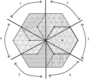
Fig. 7.6: Division of overlapped regions.
After selecting one hexagon, the translation of the reference vector V7* has to be done toward the center of this hexagon, as indicated in Fig. 7.7. This translation is done by subtracting the center vector of the selected hexagon from the original reference vector. Table 7.3 gives the components d and q of the reference voltage V4* after translation, for all the six hexagons. Index (3), (4), or (7) above the components indicate three-, four-, or seven-level cases, respectively.

Fig. 7.7: First translation of the reference voltage vector.
Tab. 7.3: First correction of the reference voltage vector.
| S | ||
| 1 | ||
| 2 | ||
| 3 | ||
| 4 | ||
| 5 | ||
| 6 |
7.2.3Second correction of the reference voltage vector
Having the selected four-level inverter diagram and the location of the translated vector, one hexagon is selected among the six small hexagons that contain this four-level diagram, as shown in Fig. 7.4. Here, the overlapped regions are equally divided between the two hexagons. After the selection of one hexagon, we translate the reference vector V4* toward the center of this hexagon, as indicated in Fig. 7.8.

Fig. 7.8: Second translation of the reference voltage vector.
This translation is done by subtracting the center vector of the selected hexagon from the original reference vector. Table 7.4 gives the components d and q of the reference voltage V3* after translation, for all the six hexagons.
Tab. 7.4: Second correction of the reference voltage vector.
| S | ||
| 1 | ||
| 2 | ||
| 3 | ||
| 4 | ||
| 5 | ||
| 6 |
7.2.4Third correction of the reference voltage vector
After selection of the three-level inverter diagram and the location of the translated vector, one hexagon is selected among the six small hexagons that contain this three-level diagram, as shown in Fig. 7.5. Here also the overlapped regions are equally divided between the two hexagons. After selection of one hexagon, the translation of the reference vector V3* has to be done toward the center of this hexagon, as indicated in Fig. 7.9.

Fig. 7.9: Third translation of the reference voltage vector.
This translation is done by subtracting the center vector of the selected hexagon from the original reference vector. Table 7.5 gives the components d and q of the reference voltage V2* after translation, for all the six hexagons.
Tab. 7.5: Third correction of the reference voltage vector.
| S | ||
| 1 | ||
| 2 | ||
| 3 | ||
| 4 | ||
| 5 | ||
| 6 |
7.2.5Determination of switching times
Once the corrected reference voltage V2* and the corresponding hexagon are determined, we can apply the conventional two-level SVPWM method to calculate the dwelling times; the only difference between the two-level SVPWM and the five-level SVPWM is factor 6 appearing at the first two equations, as shown in Eq. (7.1). The remaining procedure is implemented like the conventional two-level inverter SVPWM method and two level equivalent pulses are obtained.
This process is implemented by first considering each four-level decomposed space vector diagram of seven-level space vector diagram based on the value of s. Second, each four-level space vector diagram is further decomposed into 6 three-level space vector diagrams. Finally, each three-level space vector diagram is further decomposed into 6 two-level space vector diagrams, and the switching states of seven-level space vector diagram are changed into its equivalent two-level switching states. The optimum sequence of these three states is selected to minimize the total number of switching transitions and fully optimize the harmonic profile of the output voltage. Note that from the two-level space vector modulation theory, it is well known that these sequences should be reversed in the next switching interval for minimum harmonic impact.
The SVPWM algorithm for multilevel inverters using the decomposition method is proposed. In this method, the space vector diagram of multilevel inverter is decomposed into several space vector diagrams of the two-level inverters. The validity of the proposed method is verified for the three-, five-, and seven-level inverters by simulation. The simulation parameters and specifications of induction motor used in this method are given in Appendix IV. The results of the three-level inverter are shown in Figs. 7.10 to 7.16. The pole voltages, phase voltages, and line voltages are shown in Figs. 7.10 to 7.12, respectively. The stator currents, rotor speed, and torque of the three-level inverter fed induction motor are shown in Figs. 7.13 to 7.15, respectively. The output voltage harmonic spectrum and total harmonic distortion (THD) of the three-level inverter are shown in Fig. 7.16.
The results of the five-level inverter are shown in Figs. 7.17 to 7.23. The pole voltages, phase voltages, and line voltages are shown in Figs. 7.17 to 7.19, respectively. The stator currents, rotor speed, and torque of the five-level inverter fed induction motor are shown in Figs. 7.20 to 7.22, respectively. The output voltage harmonic spectrum and the THD of the five-level inverter are shown in Fig. 7.23. The results of the seven-level inverter are shown in Figs. 7.24 to 7.30. The pole voltages, phase voltages, and line voltages are shown in Figs. 7.24 to 7.26, respectively. The stator currents, rotor speed, and torque of the seven-level inverter fed induction motor are shown in Figs. 7.27 to 7.29, respectively. The output voltage harmonic spectrum and the THD of the five-level inverter are shown in Fig. 7.30. The obtained THD for the three-, five-, and seven-level inverters is 5.93%, 2.79%, and 1.51%, respectively, which is much less as compared with other conventional SVPWM techniques.

Fig. 7.10: Pole voltages of the three-level inverter.

Fig. 7.11: Phase voltages of the three-level inverter.

Fig. 7.12: Line-to-line voltages of the three-level inverter.

Fig. 7.13: Stator currents of the three-level inverter fed induction motor.

Fig. 7.14: Speed response of the three-level inverter fed induction motor.

Fig. 7.15: Torque response of the three-level inverter fed induction motor.

Fig. 7.16: Output line voltage (and its harmonic spectrum) of the three-level inverter.

Fig. 7.17: Pole voltages of the five-level inverter.

Fig. 7.18: Phase voltages of the five-level inverter.

Fig. 7.19: Line-to-line voltages of the five-level inverter.

Fig. 7.20: Stator currents of the five-level inverter fed induction motor.

Fig. 7.21: Speed response of the five-level inverter fed induction motor.

Fig. 7.22: Torque response of the five-level inverter fed induction motor.

Fig. 7.23: Output line voltage (and its harmonic spectrum) of the five-level inverter.

Fig. 7.24: Pole voltages of the seven-level inverter.

Fig. 7.25: Phase voltages of the seven-level inverter.

Fig. 7.26: Line-to-line voltages of the seven-level inverter.

Fig. 7.27: Stator currents of the seven-level inverter fed induction motor.

Fig. 7.28: Speed response of the seven-level inverter fed induction motor.

Fig. 7.29: Torque response of the seven-level inverter fed induction motor.

Fig. 7.30: Output line voltage (and its harmonic spectrum) of the seven-level inverter.
In this chapter, the SVPWM for the multilevel inverter using the decomposition method has been proposed and described for a seven-level inverter. In this method, the space vector diagram of the multilevel inverter is decomposed into several space vector diagrams of the two-level inverter. After decomposition, all the remaining necessary procedures for multilevel inverter are done like conventional two-level inverter. The dwelling times of the voltage vectors are calculated at the same manner as the two-level inverter. Thus, the proposed method reduces the algorithm complexity and execution time. The results are obtained for the three-, five-, and seven-level inverters. The obtained THD with the proposed method for the three-, five-, and seven-level inverters is 5.93%, 2.79%, and 1.51%, respectively. The phase voltage, torque, speed, and current responses are greatly improved.