
Chapter 10. Integer-N Frequency Synthesizers
The oscillators used in RF transceivers are usually embedded in a “synthesizer” environment so as to precisely define their output frequency. Synthesizer design has for decades proved a difficult task, leading to hundreds of RF synthesis techniques. RF synthesizers typically employ phase-locking and must deal with the generic PLL issues described in Chapter 9. In this chapter, we study one class called “integer-N” synthesizers. The chapter outline is shown below. The reader is encouraged to first review Chapters 8 and 9.

10.1 General Considerations
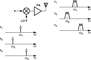
Recall from Chapter 3 that each wireless standard provides a certain number of frequency channels for communication. For example, Bluetooth has 80 1-MHz channels in the range of 2.400 GHz to 2.480 GHz. At the beginning of each communication session, one of these channels, fj, is allocated to the user, requiring that the LO frequency be set (defined) accordingly (Fig. 10.1). The synthesizer performs this precise setting.
Figure 10.1 Setting of LO frequency for each received channel.

The reader may wonder why a synthesizer is necessary. It appears that the control voltage of a VCO can be simply changed to establish the required LO frequency. The VCOs studied in Chapter 8 are called “free-running” because, for a given control voltage, their output frequency is defined by the circuit and device parameters. The frequency therefore varies with temperature, process, and supply voltage. It also drifts with time due to low-frequency phase noise components. For these reasons, VCOs are controlled by a phase-locked loop such that their output frequency can track a precise reference frequency (typically derived from a crystal oscillator).
The high precision expected of the LO frequency should not come as a surprise. After all, narrow, tightly-spaced channels in wireless standards tolerate little error in transmit and receive carrier frequencies. For example, as shown in Fig. 10.2, a slight shift leads to significant spillage of a high-power interferer into a desired channel. We know from the wireless standards studied in Chapter 3 that the channel spacing can be as small as 30 kHz while the center frequency lies in the gigahertz range.
Figure 10.2 Effect of LO frequency error in TX.
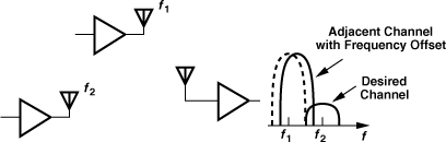
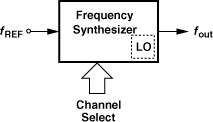
Figure 10.3 shows the conceptual picture we have thus far formed of a synthesizer. The output frequency is generated as a multiple of a precise reference, fREF, and this multiple is changed by the channel selection command so as to cover the carrier frequencies required by the standard.
Figure 10.3 Generic frequency synthesizer.
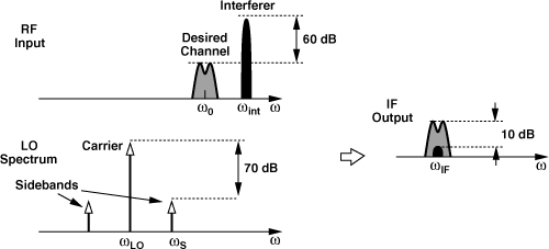
In addition to accuracy and channel spacing, several other aspects of synthesizers impact a transceiver’s performance: phase noise, sidebands, and “lock time.” We studied the effect of phase noise in Chapter 8 and deal with sidebands and lock time here. We know that, if the control voltage of a VCO is periodically disturbed, then the output spectrum contains sidebands symmetrically disposed around the carrier. This indeed occurs if a VCO is placed in a phase-locked loop and experiences the ripple produced by the PFD and CP nonidealities. We therefore wish to understand the effect of such sidebands (“spurs”). Illustrated in Fig. 10.4, the effect of sidebands is particularly troublesome in the receiver path. Suppose the synthesizer (the LO) output consists of a carrier at ωLO and a sideband at ωS, while the received signal is accompanied by an interferer at ωint. Upon downconversion mixing, the desired channel is convolved with the carrier and the interferer with the sideband. If ωint − ωS = ω0 − ωLO (=ωIF), then the downconverted interferer falls atop the desired channel. For example, if the interferer is 60 dB above the desired signal and the sideband is 70 dB below the carrier, then the corruption at the IF is 10 dB below the signal—barely an acceptable value in some standards.
Figure 10.4 Reciprocal mixing.
When the digital channel selection command in Fig. 10.3 changes value, the synthesizer takes a finite time to settle to a new output frequency (Fig. 10.6). Called the “lock time” for synthesizers that employ PLLs, this settling time directly subtracts from the time available for communication. The following example elaborates on this point.
Figure 10.6 Frequency settling during synthesizer lock period.

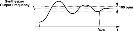
Lock times required in typical RF systems vary from a few tens of milliseconds to a few tens of microseconds. (Exceptional cases such as ultra-wideband systems stipulate a lock time of less than 10 ns.) But how is the lock time defined? Illustrated in Fig. 10.8, the lock time is typically specified as the time required for the output frequency to reach within a certain margin (e.g., 100 ppm) around its final value.
Figure 10.8 Definition of synthesizer lock time.
10.2 Basic Integer-N Synthesizer
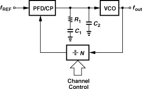
Recall from Chapter 9 that a PLL employing a feedback divide ratio of N multiplies the input frequency by the same factor. Based on this concept, integer-N synthesizers produce an output frequency that is an integer multiple of the reference frequency (Fig. 10.9). If N increases by 1, then fout increases by fREF; i.e., the minimum channel spacing is equal to the reference frequency.
Figure 10.9 Integer-N synthesizer.
How does the synthesizer of Fig. 10.9 cover a desired frequency range, f1 to f2? The divide ratio must be programmable from, say, N1 to N2 so that N1fREF = f1 and N2fREF = f2. We therefore recognize two conditions for the choice of fREF: it must be equal to the desired channel spacing and it must be the greatest common divisor of f1 and f2. The choice may be dominated by one of the two conditions; e.g., the minimum channel spacing may be smaller than the greatest common divisor of f1 and f2.
Solution:
(a) Shown in Fig. 10.10(a), the LO range extends from the center of the first channel, 2400.5 MHz, to that of the last, 2479.5 MHz. Thus, even though the channel spacing is 1 MHz, fREF must be chosen equal to 500 kHz. Consequently, N1 = 4801 and N2 = 4959.
Figure 10.10 Bluetooth LO frequency range for (a) direct and (b) sliding-IF downconversion.

(b) As illustrated in Fig. 10.10(b), in this case the channel spacing and the center frequencies are multiplied by 2/3. Thus, fREF = 1/3 MHz, N1 = 4801, and N2 = 4959.
The simplicity of the integer-N synthesizer makes it an attractive choice. Behaving as a standard PLL, this architecture lends itself to the analyses carried out in Chapter 9. In particular, the PFD/CP nonidealities and design techniques described in Chapter 9 directly apply to integer-N synthesizers.
10.3 Settling Behavior
Our study of PLL dynamics in Chapter 9 has dealt with frequency or phase changes at the input, a rare event in RF synthesizers. Instead, the transients of interest are those due to (1) a change in the feedback divide ratio, i.e., as the synthesizer hops from one channel to another, or (2) the startup switching, i.e., the synthesizer has been off to save power and is now turned on.
Let us consider the case of channel switching. Interestingly, a small change in N yields the same transient behavior as does a small change in the input frequency. This can be proved with the aid of the feedback system shown in Fig. 10.11, where the feedback factor A changes by a small amount ![]() at t = 0. The output after t = 0 is equal to
at t = 0. The output after t = 0 is equal to
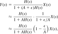
implying that the change is equivalent to multiplying X(s) by (1 − ![]() /A) while retaining the same transfer function. Since in the synthesizer environment, x(t) (the input frequency) is constant before t = 0, i.e., x(t) = f0, we can view multiplication by (1 −
/A) while retaining the same transfer function. Since in the synthesizer environment, x(t) (the input frequency) is constant before t = 0, i.e., x(t) = f0, we can view multiplication by (1 − ![]() /A) as a step function from f0 to f0(1 −
/A) as a step function from f0 to f0(1 − ![]() /A),1 i.e., a frequency jump of −(
/A),1 i.e., a frequency jump of −(![]() /A)f0.
/A)f0.
Figure 10.11 Effect of changing the feedback factor.

The foregoing analysis suggests that, when the divide ratio changes, the loop responds as if an input frequency step were applied, requiring a finite time to settle within an acceptable margin around its final value. As shown in Fig. 10.12, the worst case occurs when the synthesizer output frequency must go from the first channel, N1fREF, to the last, N2 fREF, or vice versa.
Figure 10.12 Worst-case synthesizer settling.
In order to estimate the settling time, we combine the above result with the equations derived in Chapter 9, assuming N2 − N1 ![]() N1. If the divide ratio jumps from N1 to N2, this change is equivalent to an input frequency step of Δωin = (N2 − N1)ωREF/N1.
N1. If the divide ratio jumps from N1 to N2, this change is equivalent to an input frequency step of Δωin = (N2 − N1)ωREF/N1.
We must also note that (a) the PLL settling equations are multiplied by the divide ratio, N1 (≈ N2) in an integer-N synthesizer, and (b) to obtain the settling time, the settling equations must be normalized to the final frequency, N2ωREF. For the normalized error to fall below a certain amount, α, we have
![]()
where
For example, if ![]() , Eqs. (10.7) and (10.8) yield
, Eqs. (10.7) and (10.8) yield
![]()
where ts denotes the settling time. A sufficient condition for the settling is that the exponential envelope decay to small values:
![]()
where the factor of ![]() represents the resultant of the cosine and the sine in Eq. (10.11). We therefore obtain the settling time for a normalized error of α as
represents the resultant of the cosine and the sine in Eq. (10.11). We therefore obtain the settling time for a normalized error of α as
![]()
A 900-MHz GSM synthesizer operates with fREF = 200 kHz and provides 128 channels. If ![]() , determine the settling time required for a frequency error of 10 ppm.
, determine the settling time required for a frequency error of 10 ppm.
Solution:
![]()
![]()
While this relation has been derived for ![]() , it provides a reasonable approximation for other values of ζ up to about unity.
, it provides a reasonable approximation for other values of ζ up to about unity.
![]()
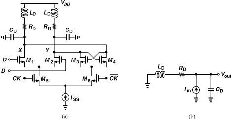
As observed in Chapter 9 and in this section, the loop bandwidth trades with a number of critical parameters, including the settling time and the suppression of the VCO phase noise. Another important trade-off is that between the loop bandwidth and the magnitude of the reference sidebands. In the locked condition, the charge pump inevitably disturbs the control voltage at every phase comparison instant, modulating the VCO. In order to reduce this disturbance, the second capacitor (C2 in Fig. 10.9) must be increased, and so must the main capacitor, C1, because C2 ≤ 0.2C1.
The principal drawback of the integer-N architecture is that the output channel spacing is equal to the input reference frequency. We recognize that both the lock time (≈ 100 input cycles) and the loop bandwidth (≈ 1/10 of the input frequency) are tightly related to the channel spacing. Consequently, synthesizers designed for narrow-channel applications suffer from a long lock time and only slightly reduce the VCO phase noise.
10.4 Spur Reduction Techniques
The trade-off between the loop bandwidth and the level of reference spurs has motivated extensive work on methods of spur reduction without sacrificing the bandwidth. Indeed, the techniques described in Chapter 9 alleviating issues such as charge sharing, channel-length modulation, and Up and Down current mismatch fall in this category. In this section, we study additional approaches that lower the ripple on the control voltage.
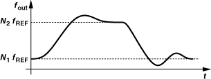
A key point in devising spur reduction techniques is that the disturbance of the control voltage occurs primarily at the phase comparison instant. In other words, Vcont is disturbed for a short duration and remains relatively constant for the rest of the input period. We therefore surmise that the output sidebands can be lowered if Vcont is isolated from the disturbance for that duration. For example, consider the arrangement shown in Fig. 10.13(a), where S1 turns off just before phase comparison begins and turns on slightly after the disturbance is finished. As a result, C2 senses only the stable value at X and holds this value when S1 is off. (The charge injection and clock feedthrough of S1 still slightly disturb Vcont.)
Figure 10.13 Masking the ripple at node X by insertion of a switch, (a) with the second capacitor tied to Vcont, (b) with the main RC section tied to Vcont.
Unfortunately, the arrangement of Fig. 10.13(a) leads to an unstable PLL. To understand this point, we recognize that the isolation of Vcont from the disturbance also eliminates the role of R1. Since we keep S1 off until the disturbance is finished, the voltage sensed by C2 when S1 turns on is independent of the value of R1. That is, the circuit’s behavior does not change if R1 = 0. (As explained in Chapter 9, to create a zero, R1 must produce a slight jump on the control voltage each time a finite, random phase error is detected.)
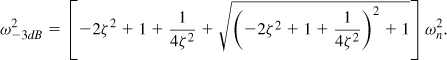
Let us now swap the two sections of the loop filter as shown in Fig. 10.13(b), where S1 is still switched according to the waveforms in Fig. 10.13(a). Can this topology yield a stable PLL? Yes, it can. Upon experiencing a jump due to a finite phase error, node X delivers this jump to Vcont after S1 turns on. Thus, the role of R1 is maintained. On the other hand, the short-duration disturbance due to PFD and CP nonidealities is “masked” by S1, thereby leading to lower sidebands at the output [1, 2]. In practice, about half of C2 is tied to Vcont so as to suppress the charge injection and clock feedthrough of S1 [1, 2]. This “sampling loop filter” employs complementary transistors for S1 to accommodate a rail-to-rail control voltage.
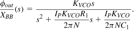
In order to arrive at another method of spur reduction, let us return to the open-loop transfer function of a type-II second-order PLL,
![]()
and recall from Chapter 9 that R1 is added in series with C1 so as to create a zero in Hopen(s). We may then ask, is it possible to add a constant to KVCO/s rather than to 1/(C1s)? That is, can we realize
![]()
so as to obtain a zero? The loop now contains a zero at KVCO/K1, whose magnitude can be chosen to yield a reasonable damping factor.
Before computing the damping factor, we ponder the meaning of K1 in Eq. (10.18). Since K1 simply adds to the output phase of the VCO, we may surmise that it denotes a constant delay after the VCO. But the transfer function of such a delay [of the form exp(−K1s)] would be multiplied by KVCO/s. To avoid this confusion, we construct a block diagram representing Eq. (10.18) [Fig. 10.14(a)], recognizing that KVCO/s + K1 is, in fact, the transfer function from Vcont to φ1, i.e.,
![]()
Figure 10.14 (a) Stabilization of PLL by adding K1 to the transfer function of VCO, (b) realization using a variable-delay stage.

That is, K1 denotes a block that is controlled by Vcont. Indeed, K1 represents a variable-delay stage [3] having a “gain” of K1:
![]()
where Td is the delay of the stage [Fig. 10.14(b)].
The key advantage of the topology shown in Fig. 10.14(b) over a standard type-II PLL is that, by avoiding the resistor in series with C1, it allows this capacitor to absorb the PFD/CP nonidealities. By contrast, in the standard PLL, only the smaller capacitor plays this role.
In order to determine the damping factor, we use Eq. (10.18) to write the closed-loop transfer function:

It follows that
In Problem 10.1, we prove that, with a feedback divider, these parameters are revised as
![]()
Equation (10.25) implies that K1 must be scaled in proportion to N so as to maintain a reasonable value for ζ, a difficult task because delay stages that accommodate high frequencies inevitably exhibit a short delay. The architecture is therefore modified to that shown in Fig. 10.15, where the variable delay line appears after the divider [3]. The reader can show that
![]()
A retiming flipflop can be inserted between the delay line and the PFD to remove the phase noise of the former (Section 10.6.7).
Figure 10.15 Stabilization of an integer-N synthesizer.

10.5 PLL-Based Modulation
In addition to the modulator and transmitter architectures introduced in Chapter 4, a number of other topologies can be realized that merge the modulation and frequency synthesis functions. We study two in this section and a few more in Chapter 12.
10.5.1 In-Loop Modulation
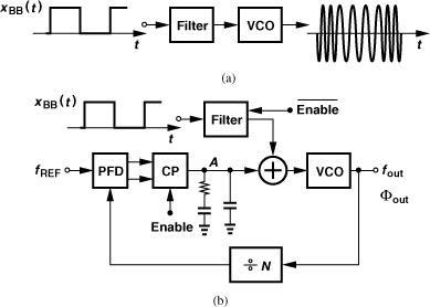
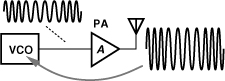
In addition to frequency synthesis, PLLs can also perform modulation. Recall from Chapter 3 that FSK and GMSK modulation can be realized by means of a VCO that senses the binary data. Figure 10.16(a) depicts a general case where the filter smoothes the time-domain transitions to some extent, thereby reducing the required bandwidth.2 The principal issue here is the poor definition of the carrier frequency: the VCO center frequency drifts with time and temperature with no bound. One remedy is to phase-lock the VCO periodically to a reference so as to reset its center frequency. Illustrated in Fig. 10.16(b), such a system first disables the baseband data path and enables the PLL, allowing fout to settle to NfREF. Next, the PLL is disabled and xBB(t) is applied to the VCO.
Figure 10.16 (a) Open-loop modulation and (b) in-loop modulation of VCO.
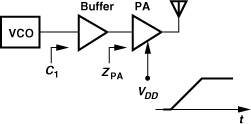
The arrangement of Fig. 10.16(b) requires periodic “idle” times during the communication to phase-lock the VCO, a serious drawback. Also, the output signal bandwidth depends on KVCO, a poorly-controlled parameter. Moreover, the free-running VCO frequency may shift from NfREF due to a change in its load capacitance or supply voltage. Specifically, as depicted in Fig. 10.17, if the power amplifier is ramped at the beginning of transmission, its input impedance ZPA changes considerably, thus altering the capacitance seen at the input of the buffer (“load pulling”). Also, upon turning on, the PA draws a very high current from the system supply, reducing its voltage by tens or perhaps hundreds of millivolts and changing the VCO frequency (“supply pushing”).
Figure 10.17 Variation of buffer input impedance during PA ramp-up.
To alleviate the foregoing issues, the VCO can remain locked while sensing the baseband data. That is, the PLL in Fig. 10.16(b) continuously monitors and corrects the VCO output (i.e., the CP is always enabled). Of course, to impress the data upon the carrier successfully, the design must select a very slow loop so that the desired phase modulation at the output is not corrected by the PLL. Called “in-loop modulation,” this approach offers two advantages over the quadrature upconversion techniques studied in Chapter 4. First, in contrast to a quadrature GMSK modulator, it requires much less processing of the baseband data. Second, it obviates the need for the quadrature phases of the LO. Of course, this method can be applied only to constant-envelope modulation schemes.
In-loop modulation entails two drawbacks: (1) due to the very small PLL bandwidth, the VCO phase noise remains mostly uncorrected, and (2) the modulated signal bandwidth is a function of KVCO, a process- and temperature-dependent parameter.
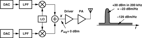
10.5.2 Modulation by Offset PLLs
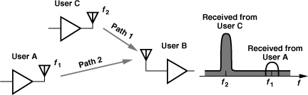
A stringent requirement imposed by GSM has led to a transmitter architecture that employs a PLL with “offset mixing.” The requirement relates to the maximum noise that a GSM transmitter is allowed to emit in the GSM receive band, namely, −129 dBm/Hz. Illustrated in Fig. 10.19 is a situation where the TX noise becomes critical: user B receives a weak signal around f1 from user A while user C, located in the close proximity of user B, transmits a high power around f2 and significant broadband noise. As shown here, the noise transmitted by user C corrupts the desired signal around f1.
Figure 10.19 Problem of transmitted noise in receiver band.
The problem of broadband noise is particularly pronounced in direct-conversion transmitters. As depicted in Fig. 10.20, each stage in the signal path contributes noise, producing high output noise in the RX band even if the baseband LPF suppresses the out-of-channel DAC output noise. In Problem 10.2, we observe that the far-out phase noise of the LO also manifests itself as broadband noise at the PA output.
Figure 10.20 Noise amplification in a direct-conversion TX along with typical values.
Solution:
The noise floor must be 30 dB lower than that at the PA output, i.e., −159 dBm/Hz in a 50-Ω system ![]() . Such a low level dictates very small load resistors for the upconversion mixers. In other words, it is simply impractical to maintain a sufficiently low noise floor at each point along the TX chain.
. Such a low level dictates very small load resistors for the upconversion mixers. In other words, it is simply impractical to maintain a sufficiently low noise floor at each point along the TX chain.
In order to reduce the TX noise in the RX band, a duplexer filter can be interposed between the antenna and the transceiver. (Recall from Chapter 4 that a duplexer is otherwise unnecessary in GSM because the TX and RX do not operate simultaneously.) However, the duplexer loss (2–3 dB) lowers the transmitted power and raises the receiver noise figure.
Alternatively, the upconversion chain can be modified so as to produce a small amount of broadband noise. For example, consider the topology shown in Fig. 10.21(a), where the baseband signal is upconverted and applied to a PLL. If the PLL bandwidth is only large enough to accommodate the signal, then xout(t) ≈ x1(t), but the broadband noise traveling to the antenna arises primarily from the far-out phase noise of the VCO. That is, unlike the TX chain in Fig. 10.20, this architecture need only minimize the broadband noise of one building block. Note that x1(t) has a constant envelope.
Figure 10.21 (a) Noise filtration by means of a PLL, (b) use of ÷N in feedback, (c) offset-PLL architecture.

The above approach dictates that the PFD and CP operate at the carrier frequency, a relatively difficult requirement. We therefore add a feedback divider to the PLL to proportionally reduce the carrier frequency of x1(t) [Fig. 10.21(b)]. If x1(t) = A1 cos[ω1t + φ(t)], where φ(t) denotes GMSK or other types of frequency or phase modulation, and if the PLL bandwidth is large enough, then
![]()
Unfortunately, the PLL multiplies the phase by a factor of N, altering the signal bandwidth and modulation.
Let us now modify the architecture as shown in Fig. 10.21(c) [4]. Here, an “offset mixer,” MX1, downconverts the output to a center frequency of fREF, and the result is separated into quadrature phases, mixed with the baseband signals, and applied to the PFD.4 With the loop locked, x1(t) must become a faithful replica of the reference input, thus containing no modulation. Consequently, yI(t) and yQ(t) “absorb” the modulation information of the baseband signal. This architecture is called an “offset-PLL” transmitter or a “translational” loop.
The local oscillator waveform driving the offset mixer in Fig. 10.21(c) must, of course, be generated by another PLL according to the synthesis methods and concepts studied thus far in this chapter. However, the presence of two VCOs on the same chip raises concern with respect to mutual injection pulling between them. To ensure a sufficient difference between their frequencies, the offset frequency, fREF, must be chosen high enough (e.g., 20% of fLO). Additionally, two other reasons call for a large offset: (1) the stages following MX1 must not degrade the phase margin of the overall loop, and (2) the center frequency of the 90° phase shift must be much greater than the signal bandwidth to allow accurate quadrature separation. Another variant of offset PLLs returns the output of the mixer directly to the PFD [5].
10.6 Divider Design
The feedback divider used in integer-N synthesizers presents interesting design challenges: (1) the divider modulus, N, must change in unity steps, (2) the first stage of the divider must operate as fast as the VCO, (3) the divider input capacitance and required input swing must be commensurate with the VCO drive capability, (4) the divider must consume low power, preferably less than the VCO. In this section, we describe divider designs that meet these requirements.
It is important to note that divider design typically assumes the VCO to have certain voltage swings and output drive capability and, as such, must be carried out in conjunction with the VCO design. Shown in Fig. 10.23 is an example where the VCO runs at twice the carrier frequency to avoid injection-pulling and is followed by a ÷2 stage. This divider may need to drive a considerable load capacitance, CL, making it necessary to use wide transistors therein and hence present a large capacitance, Cdiv, to the VCO. A buffer can be inserted at the input and/or output of the divider but at the cost of greater power dissipation.
Figure 10.23 Load seen by divider in a transceiver.
10.6.1 Pulse Swallow Divider
A common realization of the feedback divider that allows unity steps in the modulus is called the “pulse swallow divider.” Shown in Fig. 10.24, the circuit consists of three blocks:
1. A “dual-modulus prescaler”; this counter provides a divide ratio of N + 1 or N according to the logical state of its “modulus control” input.
2. A “swallow counter”; this circuit divides its input frequency by a factor of S, which can be set to a value of 1 or higher in unity steps by means of the digital input.5 This counter controls the modulus of the prescaler and also has a reset input.
3. A “program counter”; this divider has a constant modulus, P. When the program counter “fills up” (after it counts P pulses at its input), it resets the swallow counter.
Figure 10.24 Pulse swallow divider.
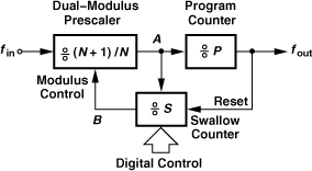
We now show that the overall pulse swallow divider of Fig. 10.24(a) provides a divide ratio of NP + S. Suppose all three dividers begin from reset. The prescaler counts by N + 1, giving one pulse to the swallow counter (at point A) for every N + 1 pulses at the main input. The program counter counts the output pulses of the prescaler (point B). This continues until the swallow counter fills up, i.e., it receives S pulses at its input. [The main input therefore receives (N + 1)S pulses.] The swallow counter then changes the modulus of the prescaler to N and begins from zero again. Note that the program counter has thus far counted S pulses, requiring another P − S pulses to fill up. Now, the prescaler divides by N, producing P − S pulses so as to fill up the program counter. In this mode, the main input must receive N(P − S) pulses. Adding the total number of the pulses at the prescaler input in the two modes, we have (N + 1)S + N(P − S) = NP + S. That is, for every NP + S pulses at the main input, the program counter generates one pulse at the output. The operation repeats after the swallow counter is reset. Note that P must be greater than S.
Sensing the high-frequency input, the prescaler proves the most challenging of the three building blocks. For this reason, numerous prescaler topologies have been introduced. We study some in the next section. As a rule of thumb, dual-modulus prescalers are about a factor of two slower than ÷2 circuits.
Figure 10.25 (a) Use of ÷2 stage to relax the speed required of pulse swallow divider, (b) effect on output phase noise, (c) location of reference spurs with and without the ÷2 stage.

Solution:
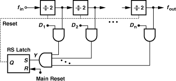
The swallow counter is typically designed as an asynchronous circuit for the sake of simplicity and power savings. Figure 10.26 shows a possible implementation, where cascaded ÷2 stages count the input and the NAND gates compare the count with the digital input, DnDn−1...D1. Once the count reaches the digital input, Y goes high, setting the RS latch. The latch output then disables the ÷2 stages. The circuit remains in this state until the main reset is asserted (by the program counter).
Figure 10.26 Swallow counter realization.
An alternative approach to realizing the feedback divider in a synthesizer is described in [7]. This method incorporates ÷2/3 stages in a modular form so as to reduce the design complexity. Shown in Fig. 10.27, the divider employs n ÷2/3 blocks, each receiving a modulus control from the next stage (except for the last stage). The digital inputs set the
Figure 10.27 Modular divider realizing multiple divide ratios.
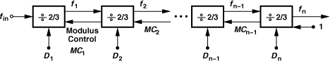
overall divide ratio according to
![]()
10.6.2 Dual-Modulus Dividers
As mentioned above, dual-modulus prescalers pose the most difficult challenge in divider design. We also note from our analysis of the pulse swallow divider in Section 10.6.1 that the modulus change must be instantaneous, an obvious condition but not necessarily met in all dual-modulus designs. As explained in the following sections, circuits such as the Miller divider and injection-locked dividers take a number of input cycles to reach the steady state.
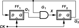
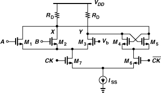
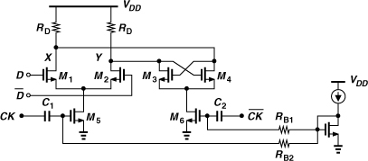
Let us begin our study of dual-modulus prescalers with a divide-by-2/3 circuit. Recall from Chapter 4 that a ÷2 circuit can be realized as a D-flipflop placed in a negative feedback loop. A ÷3 circuit, on the other hand, requires two flipflops. Shown in Fig. 10.28 is an example,6 where an AND gate applies ![]() to the D input of FF2. Suppose the circuit begins with
to the D input of FF2. Suppose the circuit begins with ![]() . After the first clock, Q1 assumes the value of
. After the first clock, Q1 assumes the value of ![]() (ZERO), and
(ZERO), and ![]() the value of
the value of ![]() (ONE). In the next three cycles,
(ONE). In the next three cycles, ![]() goes to 10, 11, and 01. Note that the state
goes to 10, 11, and 01. Note that the state ![]() does not occur again because it would require the previous values of
does not occur again because it would require the previous values of ![]() and X to be ZERO and ONE, respectively, a condition prohibited by the AND gate.
and X to be ZERO and ONE, respectively, a condition prohibited by the AND gate.
Figure 10.28 Divide-by-3 circuit.
Solution:
Figure 10.29 Implementation of ÷3 circuit using a NOR gate: (a) use of Q2 with a bubble at the NAND input and FF1 input, (b) bubble moved from input of FF1 to its output, (c) final realization.
Solution:
We draw the circuit as in Fig. 10.30(a), explicitly showing the two latches within FF2. Suppose CK is initially low, L1 is opaque (in the latch mode), and L2 is transparent (in the sense mode). In other words, ![]() has just changed. When CK goes high and L1 begins to sense, the value of
has just changed. When CK goes high and L1 begins to sense, the value of ![]() must propagate through G1 and L1 before CK can fall again. Thus, the delay of G1 enters the critical path. Moreover, L2 must drive the input capacitance of FF1, G1, and an output buffer. These effects degrade the speed considerably, requiring that CK remain high long enough for
must propagate through G1 and L1 before CK can fall again. Thus, the delay of G1 enters the critical path. Moreover, L2 must drive the input capacitance of FF1, G1, and an output buffer. These effects degrade the speed considerably, requiring that CK remain high long enough for ![]() to propagate to Y.
to propagate to Y.
Figure 10.30 Timing and critical path in ÷3 circuit.

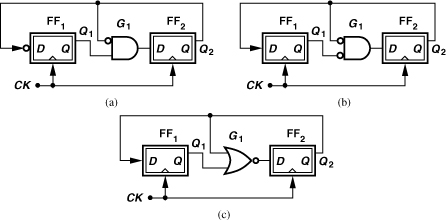
The circuit of Fig. 10.28 can now be modified so as to have two moduli. Illustrated in Fig. 10.31, the ÷2/3 circuit employs an OR gate to permit ÷3 operation if the modulus control, MC, is low (why?) or ÷2 operation if it is high. In the latter case, only FF2 divides the clock by 2 while FF1 plays no role. Thus, the output can be provided by only FF2.
Figure 10.31 Divide-by-2/3 circuit.

Solution:
While saving power, turning off FF1 may prohibit instantaneous modulus change because when FF1 turns on, its initial state is undefined, possibly requiring an additional clock cycle to reach the desired value. For example, the overall circuit may begin with ![]() .
.
It is possible to rearrange the ÷2/3 stage so as to reduce the loading on the second flipflop. Illustrated in Fig. 10.32 [6], the circuit precedes each flipflop with a NOR gate. If MC is low, then ![]() is simply inverted by G2—as if FF2 directly followed FF1. The circuit thus reduces to the ÷3 stage depicted in Fig. 10.29(c). If MC is high, Q2 remains low, allowing G1 and FF1 to divide by two. Note that the output can be provided by only FF1. This circuit has a 40% speed advantage over that in Fig. 10.31 [6].
is simply inverted by G2—as if FF2 directly followed FF1. The circuit thus reduces to the ÷3 stage depicted in Fig. 10.29(c). If MC is high, Q2 remains low, allowing G1 and FF1 to divide by two. Note that the output can be provided by only FF1. This circuit has a 40% speed advantage over that in Fig. 10.31 [6].
Figure 10.32 Divide-by-2/3 circuit with higher speed.

Figure 10.33 shows a ÷3/4 stage. If MC = ONE, G2 produces a ONE, allowing G1 to simply pass the output of FF1 to the D input of FF2. The circuit thus resembles four latches in a loop and hence divides by 4. If MC = 0, G2 passes ![]() to the input of G1, reducing the circuit to that in Fig. 10.28. We observe that the critical path (around FF2) contains a greater delay in this circuit than in the ÷3 stage of Fig. 10.28. A transistor-level design of such a divider is presented in Chapter 13.
to the input of G1, reducing the circuit to that in Fig. 10.28. We observe that the critical path (around FF2) contains a greater delay in this circuit than in the ÷3 stage of Fig. 10.28. A transistor-level design of such a divider is presented in Chapter 13.
Figure 10.33 Divide-by-3/4 circuit.

The dual-modulus dividers studied thus far employ synchronous operation, i.e., the flipflops are clocked simultaneously. For higher moduli, a synchronous core having small moduli is combined with asynchronous divider stages. Figure 10.34 shows a ÷8/9 prescaler as an example. The ÷2/3 circuit (D23) of Fig. 10.31 is followed by two asynchronous ÷2 stages, and MC1 is defined as the NAND of their outputs with the main modulus control, MC2. If MC2 is low, MC1 is high, allowing D23 to divide by 2. The overall circuit thus operates as a ÷8 circuit. If MC2 is high and the ÷2 stages begin from a reset state, then MC1 is also high and D23 divides by 2. This continues until both A and B are high, at which point MC1 falls, forcing D23 to divide by 3 for one clock cycle before A and B return to zero. The circuit therefore divides by 9 in this mode.
Figure 10.34 Divide-by-8/9 circuit.


An important issue in employing both synchronous and asynchronous sections in Fig. 10.35 is potential race conditions when the circuit divides by 15. To understand the problem, first suppose FF3 and FF4 change their output state on the rising edge of their clock inputs. If MC is low, the circuit continues to divide by 16, i.e., ![]() goes through the cycle: 01, 11, 10, 00 until both
goes through the cycle: 01, 11, 10, 00 until both ![]() and
and ![]() are low. As depicted in Fig. 10.36(a),
are low. As depicted in Fig. 10.36(a), ![]() then skips the state 00 after the state 10. Since from the time
then skips the state 00 after the state 10. Since from the time ![]() goes low until the time
goes low until the time ![]() skips one state, three CKin cycles have passed, the propagation delay through FF3 and G3 need not be less than a cycle of CKin.
skips one state, three CKin cycles have passed, the propagation delay through FF3 and G3 need not be less than a cycle of CKin.
Figure 10.36 Delay budget in the ÷15/16 circuit with FF3 and FF4 activated on (a) rising edge, and (b) falling edge of clock.

Now consider a case where FF3 and FF4 change their output state on the falling edge of their clock inputs. Then, as shown in Fig. 10.36(b), immediately after ![]()
![]() has fallen to 00, the ÷3/4 circuit must skip the state 00, mandating that the delay through FF3, FF4, and G3 be less than half of a CKin cycle. This is in general difficult to achieve, complicating the design and demanding higher power dissipation. Thus, the first choice is preferable.
has fallen to 00, the ÷3/4 circuit must skip the state 00, mandating that the delay through FF3, FF4, and G3 be less than half of a CKin cycle. This is in general difficult to achieve, complicating the design and demanding higher power dissipation. Thus, the first choice is preferable.
10.6.3 Choice of Prescaler Modulus
The pulse swallow divider of Fig. 10.24 provides a divide ratio of NP + S, allowing some flexibility in the choice of these three parameters. For example, to cover the Bluetooth channels from 2400 MHz to 2480 MHz, we can choose N = 4, P = 575, and S = 100, ..., 180, or N = 10, P = 235, and S = 50, ..., 130. (Recall that P must remain greater than S.) What trade-offs do we face in these choices? One aspect of the design calls for using a large N, and another for a small N.
Returning to the race condition studied in the ÷15/16 circuit of Fig. 10.35, we make the following observation. With the proper choice of the clock edge, D34 begins ÷4 operation as ![]() changes and continues for two more input cycles before it goes into the ÷3 mode. More generally, for a synchronous ÷(N + 1)/N circuit followed by asynchronous stages, proper choice of the clock edge allows the circuit to divide by N + 1 for N − 1 input cycles before its modulus is changed to N. This principle applies to the pulse swallow divider as well, requiring a large N so as to permit a long delay through the asynchronous stages and the feedback loop.
changes and continues for two more input cycles before it goes into the ÷3 mode. More generally, for a synchronous ÷(N + 1)/N circuit followed by asynchronous stages, proper choice of the clock edge allows the circuit to divide by N + 1 for N − 1 input cycles before its modulus is changed to N. This principle applies to the pulse swallow divider as well, requiring a large N so as to permit a long delay through the asynchronous stages and the feedback loop.

The above perspective encourages a large N for the prescaler. On the other hand, a larger prescaler modulus leads to a higher power dissipation if the stages within the prescaler incorporate current steering to operate at high speeds (Section 10.6.4). For this reason, the prescaler modulus is determined by careful simulations. It is also possible to pipeline the output of the RS latch in Fig. 10.37, thus allowing a smaller N but additional cycles for the modulus change [6].
10.6.4 Divider Logic Styles
The divider blocks in the feedback loop of a synthesizer can be realized by means of various logic styles. The choice of a divider topology is governed by several factors: the input swing (e.g., that available from the VCO), the input capacitance (e.g., that presented to the VCO), the maximum speed, the output swing (as required by the subsequent stage), the minimum speed (i.e., dynamic logic versus static logic), and the power dissipation. In this section, we study divider design in the context of different logic families.
Current-Steering Circuits
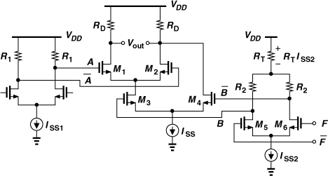
Affording the fastest circuits, current-steering logic, also known as “current-mode logic” (CML), operates with moderate input and output swings. CML circuits provide differential outputs and hence a natural inversion; e.g., a single stage serves as both a NAND gate and an AND gate. CML derives its speed from the property that a differential pair can be rapidly enabled and disabled through its tail current source.
Figure 10.38(a) shows a CML AND/NAND gate. The top differential pair senses the differential inputs, A and ![]() , and is controlled by M3 and hence by B and
, and is controlled by M3 and hence by B and ![]() . If B is high, M1 and M2 remain on,
. If B is high, M1 and M2 remain on, ![]() , and Y = A. If B is low, M1 and M2 are off, X is at VDD, and Y is pulled down by M4 to VDD − RDISS. From another perspective, we note from Fig. 10.38(b) that M1 and M3 resemble a NAND branch, and M2 and M4 a NOR branch. The circuit is typically designed for a single-ended output swing of RDISS = 300 mV, and the transistors are sized such that they experience complete switching with such input swings.
, and Y = A. If B is low, M1 and M2 are off, X is at VDD, and Y is pulled down by M4 to VDD − RDISS. From another perspective, we note from Fig. 10.38(b) that M1 and M3 resemble a NAND branch, and M2 and M4 a NOR branch. The circuit is typically designed for a single-ended output swing of RDISS = 300 mV, and the transistors are sized such that they experience complete switching with such input swings.
Figure 10.38 (a) CML NAND realization, (b) NAND and NOR branches in the circuit.

For the differential pairs in Fig. 10.38(a) to switch with moderate input swings, the transistors must not enter the triode region. For example, if M3 is in the triode region when it is on, then the swings at B and ![]() must be quite larger than 300 mV so as to turn M3 off and M4 on. Thus, the common-mode level of B and
must be quite larger than 300 mV so as to turn M3 off and M4 on. Thus, the common-mode level of B and ![]() must be below that of A and
must be below that of A and ![]() by at least one overdrive voltage, making the design of the preceding stages difficult. Figure 10.39 depicts an example, where the NAND gate is preceded by two representative CML stages. Here, A and
by at least one overdrive voltage, making the design of the preceding stages difficult. Figure 10.39 depicts an example, where the NAND gate is preceded by two representative CML stages. Here, A and ![]() swing between VDD and VDD − R1ISS1. On the other hand, by virtue of the level-shift resistor RT, B and
swing between VDD and VDD − R1ISS1. On the other hand, by virtue of the level-shift resistor RT, B and ![]() vary between VDD − RTISS2 and VDD − RTISS2 − R2ISS2. That is, RT shifts the CM level of B and
vary between VDD − RTISS2 and VDD − RTISS2 − R2ISS2. That is, RT shifts the CM level of B and ![]() by RTISS2. The addition of RT appears simple, but now the high level of F and
by RTISS2. The addition of RT appears simple, but now the high level of F and ![]() is constrained if M5 and M6 must not enter the triode region. That is, this high level must not exceed VDD − RTISS2 − R2ISS2 + VTH.
is constrained if M5 and M6 must not enter the triode region. That is, this high level must not exceed VDD − RTISS2 − R2ISS2 + VTH.
Figure 10.39 Problem of common-mode compatibility at NAND inputs.
The stacking of differential pairs in the NAND gate of Fig. 10.38(a) does not lend itself to low supply voltages. The CML NOR/OR gate, on the other hand, avoids stacking. Shown in Fig. 10.40(a), the circuit steers the tail current to the left if A or B is high, producing a low level at X and a high level at Y. Unfortunately, however, this stage operates only with single-ended inputs, demanding great attention to the CM level of A and B and the choice of Vb. Specifically, Vb must be generated such that it tracks the CM level of A and B. As illustrated in Fig. 10.40(b), Vb is established by a branch replicating the circuitry that produces A. The CM level of A is equal to VDD − R2ISS2/2, and so is the value of Vb. For very high speeds, a capacitor may be tied from Vb to VDD, thereby maintaining a solid ac ground at the gate of M3.
Figure 10.40 (a) CML NOR gate, (b) proper generation of bias voltage Vb.
At low supply voltages, we design the logic in the dividers to incorporate the NOR gate of Fig. 10.40(a) rather than the NAND circuit of Fig. 10.38(a). The ÷2/3 circuit of Fig. 10.32 exemplifies this principle. To ensure complete switching of M1-M3 in the NOR stage, the input swings must be somewhat larger than our rule of thumb of 300 mV, or the transistors must be wider.
Another commonly-used gate is the XOR circuit, shown in Fig. 10.41. The topology is identical to the Gilbert cell mixer studied in Chapter 6, except that both input ports are driven by large swings to ensure complete switching. As with the CML NAND gate, this circuit requires proper CM level shift for B and ![]() and does not easily operate with low supply voltages.
and does not easily operate with low supply voltages.
Figure 10.41 CML XOR implementation.
Figure 10.42 depicts an XOR gate that avoids stacking [8]. If A or B is high, M3 turns off; that is, ![]() . Similarly,
. Similarly, ![]() . The summation of ID3 and ID6 at node X is equivalent to an OR operation, and the flow of the sum through RD produces an inversion.
. The summation of ID3 and ID6 at node X is equivalent to an OR operation, and the flow of the sum through RD produces an inversion.
Figure 10.42 Symmetric, low-voltage XOR.

![]()
In contrast to the XOR gate of Fig. 10.41, this circuit exhibits perfect symmetry with respect to A and B, an attribute that proves useful in some applications.
While lending itself to low supply voltages, the XOR topology of Fig. 10.42 senses each of the inputs in single-ended form, facing issues similar to those of the NOR gate of Fig. 10.40(a). In other words, Vb must be defined carefully and the input voltage swings and/or transistor widths must be larger than those required for the XOR of Fig. 10.41. Also, to provide differential outputs, the circuit must be duplicated with A and ![]() (or B and
(or B and ![]() ) swapped.
) swapped.
The speed advantage of CML circuits is especially pronounced in latches. Figure 10.43(a) shows a CML D latch. The circuit consists of an input differential pair, M1-M2, a latch or “regenerative” pair, M3-M4, and a clocked pair, M5-M6. In the “sense mode,” CK is high, and M5 is on, allowing M1-M2 to sense and amplify the difference between D and ![]() . That is, X and Y track the input. In the transition to the “latch mode” (or “regeneration mode”), CK goes down, turning M1-M2 off, and
. That is, X and Y track the input. In the transition to the “latch mode” (or “regeneration mode”), CK goes down, turning M1-M2 off, and ![]() goes up, turning M3-M4 on. The circuit now reduces to that in Fig. 10.43(b), where the positive feedback around M3 and M4 regeneratively amplifies the difference between VX and VY. If the loop gain exceeds unity, the regeneration continues until one transistor turns off, e.g., VX rises to VDD and VY falls to VDD − RDISS. This state is retained until CK changes and the next sense mode begins.
goes up, turning M3-M4 on. The circuit now reduces to that in Fig. 10.43(b), where the positive feedback around M3 and M4 regeneratively amplifies the difference between VX and VY. If the loop gain exceeds unity, the regeneration continues until one transistor turns off, e.g., VX rises to VDD and VY falls to VDD − RDISS. This state is retained until CK changes and the next sense mode begins.
Figure 10.43 (a) CML latch, (b) circuit in regeneration mode, (c) circuit’s waveforms.

In order to understand the speed attributes of the latch, let us examine its voltage waveforms as the circuit goes from the sense mode to the latch mode. As shown in Fig. 10.43(c), D and ![]() cross at t = t1, and VX and VY at t = t2. Even though VX and VY have not reached their full swings at t = t3, the circuit can enter the latch mode because the regenerative pair continues the amplification after t = t3. Of course, the latch mode must be long enough for VX and VY to approach their final values. We thus conclude that the latch operates properly even with a limited bandwidth at X and Y if (a) in the sense mode, VX and VY begin from their full levels and cross, and (b) in the latch mode, the initial difference between VX and VY can be amplified to a final value of ISSRD.
cross at t = t1, and VX and VY at t = t2. Even though VX and VY have not reached their full swings at t = t3, the circuit can enter the latch mode because the regenerative pair continues the amplification after t = t3. Of course, the latch mode must be long enough for VX and VY to approach their final values. We thus conclude that the latch operates properly even with a limited bandwidth at X and Y if (a) in the sense mode, VX and VY begin from their full levels and cross, and (b) in the latch mode, the initial difference between VX and VY can be amplified to a final value of ISSRD.
Solution:
![]()
Figure 10.44 (a) CML latch in regeneration mode, (b) decomposition of CGD, and (c) circuit’s waveforms.

![]()
![]()
![]()
![]()
Of course, as VXY increases, one transistor begins to turn off and its gm falls toward zero. Note that, if gm3,4RD ![]() 1, then τreg ≈ CD/gm3,4.
1, then τreg ≈ CD/gm3,4.
It is possible to merge logic with a latch, thus reducing both the delay and the power dissipation. For example, the NOR and the master latch of FF1 depicted in Fig. 10.32 can be realized as shown in Fig. 10.46. The circuit performs a NOR/OR operation on A and B in the sense mode and stores the result in the latch mode.
Figure 10.46 CML latch incorporating NOR gate.
Design Procedure
Let us construct a ÷2 circuit by placing two D latches in a negative feedback loop (Fig. 10.47). Note that the total capacitance seen at the clock input is twice that of a single latch. The design of the circuit begins with three known parameters: the power budget, the clock swing, and the load capacitance (the input capacitance of the next stage). We then follow these steps: (1) Select ISS based on the power budget; (2) Select RDISS ≈ 300 mV; (3) Select (W/L)1,2 such that the differential pair experiences nearly complete switching for a differential input of 300 mV; (4) Select (W/L)3,4 such that the small-signal gain around the regenerative loop exceeds unity; (5) Select (W/L)5,6 such that the clocked pair steers most of the tail current with the specified clock swing. It is important to ensure that the feedback around the loop is negative (why?).
Figure 10.47 Divide-by-2 circuit consisting of two CML latches in a negative feedback loop.
The rough design thus obtained, along with the specified load capacitance, reaches a speed higher than the limit predicted by Eq. (10.49) because the voltage swings at X and Y in each latch need not reach the full amount of ISSRD for proper operation. In other words, as the clock frequency exceeds the limit given by (10.49), the output swings become smaller—up to a point where VX and VY simply do not have enough time to cross and the circuit fails.
In practice, the transistor widths may need to exceed those obtained above for three reasons: (a) the tail node voltages of M1-M2 and M3-M4 may be excessively low, driving M5-M6 into the triode region; (b) the tail node voltage of M5-M6 may be so low as to leave little headroom for ISS; and (c) at very high speeds, the voltage swings at X and Y do not reach RDISS, demanding wider transistors for steering the currents.
Solution:
Figure 10.48 Divider sensitivity plot.
Figure 10.49 Divide-by-2 circuit viewed as ring oscillator.
The stacking of the differential and regenerative pairs atop the clocked pair in Figs. 10.43 and 10.47 does not lend itself to low supply voltages. This issue is alleviated by omitting the tail current source, but the bias currents of the circuit must still be defined accurately. Figure 10.50 shows an example [9], where the bias of the clocked pair is defined by a current mirror and the clock is coupled capacitively. Without a current mirror, i.e., if the gates of M5 and M6 are directly tied to the preceding stage, the bias currents and hence the latch output swings would heavily depend on the process, temperature, and supply voltage. The value of the coupling capacitors is chosen about 5 to 10 times the gate capacitance of M5 and M6 to minimize the attenuation of the clock amplitude. Resistors RB1 and RB2 together with C1 and C2 yield a time constant much longer than the clock period. Note that capacitive coupling may be necessary even with a tail current if the VCO output CM level is incompatible with the latch input CM level (Chapter 8).
In the above circuit, large clock swings allow transistors M5 and M6 to operate in the class AB mode, i.e., their peak currents well exceed their bias current. This attribute improves the speed of the divider [9].

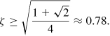
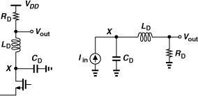
Recall from Chapter 4 that a VCO/÷2 circuit cascade proves useful in both generating the I and Q phases of the LO and avoiding injection pulling by the PA. This topology, however, dictates operation at twice the carrier frequency of interest. For the ÷2 stage to run at high frequencies, the speed of the D latch of Fig. 10.43 or 10.50 must be maximized. For example, inductive peaking raises the bandwidth at the output nodes [Fig. 10.52(a)]. From a small-signal perspective, we observe that the inductors rise in impedance at higher frequencies, allowing more of the currents produced by the transistors to flow through the capacitors and hence generate a larger output voltage. This behavior can be formulated with the aid of the equivalent circuit shown in Fig. 10.52(b). We have
![]()
Figure 10.52 (a) CML latch using inductive peaking, (b) equivalent circuit.
It is common to rewrite this transfer function as
![]()
where
![]()
is the “damping factor” and
![]()
is the “natural frequency.” To determine the −3-dB bandwidth, we equate the squared magnitude of Eq. (10.51) to (1/2)(2ζ/ωn)2(1/CD)2:
![]()
It follows that
For example, noting that ωn = 2ζ/(RDCD), we obtain ω−3dB ≈ 1.8/(RDCD) if ![]() , i.e., the bandwidth increases by 80%. If LD is increased further so that
, i.e., the bandwidth increases by 80%. If LD is increased further so that ![]() , then ω−3dB = 1.85/(RDCD). On the other hand, a conservative value of ζ = 1 yields ω−3dB = 1.41/(RDCD).
, then ω−3dB = 1.85/(RDCD). On the other hand, a conservative value of ζ = 1 yields ω−3dB = 1.41/(RDCD).
In practice, parasitics of on-chip inductors yield a bandwidth improvement less than the values predicted above. One may consider the Q of the inductor unimportant as RD appears in series with LD in Fig. 10.52. However, Q does play a role because of the finite parasitic capacitance of the inductor. For this reason, it is preferable to tie LD to VDD and RD to the output node than LD to the output node and RD to VDD; in the circuit of Fig. 10.52(a), about half of the distributed capacitance of LD is absorbed by VDD.7 This also allows a symmetric inductor and hence a higher Q.
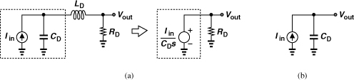
The topology depicted in Fig. 10.52(a) is called “shunt peaking” because the resistor-inductor branch appears in parallel with the output port. It is also possible to incorporate “series peaking,” whereby the inductor is placed in series with the unwanted capacitance. Illustrated in Fig. 10.53, the circuit provides the following transfer function:
![]()
which is similar to Eq. (10.50) but for a zero. The −3-dB bandwidth is computed as
![]()
where ζ and ωn are given by (10.52) and (10.53), respectively. For example, if ![]() , then
, then ![]() , i.e., series peaking increases the bandwidth by about 40%. The reader can prove that the frequency response exhibits peaking if
, i.e., series peaking increases the bandwidth by about 40%. The reader can prove that the frequency response exhibits peaking if ![]() . Note that VX/Iin satisfies the shunt peaking transfer function of (10.50).
. Note that VX/Iin satisfies the shunt peaking transfer function of (10.50).
Solution:
Let us study the behavior of the circuit at ![]() . As shown in Fig. 10.54(a), the Thevenin equivalent of Iin, CD, and LD is constructed by noting that (a) the open-circuit output voltage is equal to Iin/(CDs), and (b) the output impedance (with Iin set to zero) is zero because CD and LD resonate at ωn. It follows that Vout = Iin/(CDs) at ω = ωn, i.e., as if the circuit consisted of only Iin and CD [Fig. 10.54(b)]. Since Iin appears to flow entirely through CD, it yields a larger magnitude for Vout than if it must split between CD and RD.
. As shown in Fig. 10.54(a), the Thevenin equivalent of Iin, CD, and LD is constructed by noting that (a) the open-circuit output voltage is equal to Iin/(CDs), and (b) the output impedance (with Iin set to zero) is zero because CD and LD resonate at ωn. It follows that Vout = Iin/(CDs) at ω = ωn, i.e., as if the circuit consisted of only Iin and CD [Fig. 10.54(b)]. Since Iin appears to flow entirely through CD, it yields a larger magnitude for Vout than if it must split between CD and RD.
Figure 10.54 (a) Use of Thevenin equivalent at resonance frequency, (b) simplified view.
Circuits employing series peaking are generally more complex than the situation portrayed in Fig. 10.53. Specifically, the transistor generating Iin suffers from an output capacitance, which can be represented by CD, but the next stage also exhibits an input capacitance, which is part of CD in Fig. 10.52(a) but not included in Fig. 10.53. A more complete model is shown in Fig. 10.55(a) and two circuit examples employing series peaking are depicted in Fig. 10.55(b). The transfer function of the topology in Fig. 10.55(a) is of third order, making it difficult to compute the bandwidth, but simulations can be used to quantify the performance. Compared to shunt peaking, series peaking typically requires a smaller inductor value.
Figure 10.55 (a) Series peaking circuit driving load capacitance C2, (b) representative cases.

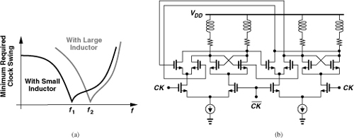
As LD increases from zero in Fig. 10.52(a), the maximum operation frequency of the divider rises. Of course, the need for at least two (symmetric) inductors for a ÷2 circuit complicates the layout. Moreover, as the value of LD becomes so large that LDω/RD (the Q of the series combination) exceeds unity at the maximum output frequency, the lower end of the operation frequency range increases. That is, the circuit begins to fail at low frequencies. Illustrated in Fig. 10.56(a), this phenomenon occurs because the circuit approaches a quadrature LC oscillator that is injection-locked to the input clock. Figure 10.56(b) shows the simplified circuit, revealing resemblance to the quadrature topology studied in Chapter 8. As the Q of the tank exceeds unity, the injection lock range of the circuit becomes narrower.
Figure 10.56 (a) Sensitivity plots with small and large load inductors, (b) inductively-peaked latch viewed as quadrature oscillator.
CML dividers have reached very high speeds in deep-submicron CMOS technologies. For example, the use of inductive peaking and class-AB operation has afforded a maximum clock frequency of 96 GHz for a ÷2 circuit [10].
True Single-Phase Clocking
Another logic style often employed in divider design is “true single-phase clocking” (TSPC) [11]. Figure 10.57(a) shows a TSPC flipflop. Incorporating dynamic logic, the circuit operates as follows. When CK is high, the first stage operates as an inverter, impressing ![]() at A and E. When CK goes low, the first stage is disabled and the second stage becomes transparent, “writing”
at A and E. When CK goes low, the first stage is disabled and the second stage becomes transparent, “writing” ![]() at B and C and hence making Q equal to A. The logical high at E and the logical low at B are degraded, but the levels at A and C ensure proper operation of the circuit.
at B and C and hence making Q equal to A. The logical high at E and the logical low at B are degraded, but the levels at A and C ensure proper operation of the circuit.
Figure 10.57 (a) TSPC flipflop, (b) response to a rising input transition when CK is low.
Does the clock completely disable each of the first two stages? Suppose CK is low. If D goes from low to high, A remains constant. On the other hand, if D falls [Fig. 10.57(b)], A rises, but the state at B does not change because M4 turns off and M6 remains off. (For a state to change, a transistor must turn on.) Now suppose CK is high, keeping M2 on and M5 off. Does a change in D propagate to Q? For example, if Q is high, and D rises, then A falls and B rises, turning M7 off. Thus, Q remains unchanged.
Since the flipflop of Fig. 10.57 contains one inversion, it can serve as a ÷2 circuit if Q is tied to D. An alternative ÷2 TSPC circuit is shown in Fig. 10.58 [11]. This topology achieves relatively high speeds with low power dissipation, but, unlike CML dividers, it requires rail-to-rail clock swings for proper operation. Moreover, it does not provide quadrature outputs. Note that (a) the circuit consumes no static power,8 and (b) as a dynamic logic topology, the divider fails at very low clock frequencies due to the leakage of the transistors. For example, if a synthesizer is designed with a reference frequency of 1 MHz, then the last few stages of the program counter in Fig. 10.24 must operate at a few megahertz, possibly failing to retain states stored on transistor capacitances.
Figure 10.58 TSPC divide-by-2 circuit.
The TSPC FF of Fig. 10.57 can readily incorporate logic at its input. For example, a NAND gate can be merged with the master latch as shown in Fig. 10.59. Thus circuits such as the ÷3 stage of Fig. 10.31 can be realized by TSPC logic as well. In the design of TSPC circuits, one observes that wider clocked devices [e.g., M2 and M5 in Fig. 10.57(a)] raises the maximum speed, but at the cost of loading the preceding stage, e.g., the VCO.
Figure 10.59 TSPC FF incorporating a NAND gate.
A variant of TSPC logic that achieves higher speeds is depicted in Fig. 10.60 [12]. Here, the first stage operates as the master D latch and the last two as the slave D latch. The slave latch is designed as “ratioed” logic, i.e., both NMOS devices are strong enough to pull down B and Q even if M4 or M6 is on. When CK is high, the first stage reduces to an inverter, the second stage forces a ZERO at B, and the third stage is in the store mode. When CK goes down, B remains low if A is high, or it rises if A is low, with Q tracking B because M7 and M6 act as a ratioed inverter.
Figure 10.60 TSPC circuit using ratioed logic.

The second and third stages in the circuit of Fig. 10.60 consume static power when their clocked transistor fights the input device. At high speeds, however, the dynamic power dominates, making this drawback less objectionable. In a typical design (with PMOS mobility about half of NMOS mobility), all transistors in the circuit can have equal dimensions, except for W5, which must be two to three times the other transistor widths to maximize the speed. The input can also incorporate logic in a manner similar to that in Fig. 10.59. This technique allows ÷2 speeds around 10 GHz and ÷3 speeds around 6 GHz in 65-nm CMOS technology. We incorporate this logic style in the design of a ÷3/4 circuit in Chapter 13.
The TSPC circuit and its variants operate with rail-to-rail swings but do not provide differential or quadrature outputs. A complementary logic style resolving this issue is described in Chapter 13.
10.6.5 Miller Divider
As explained in Section 10.6.4, CML dividers achieve a high speed by virtue of current steering and moderate voltage swings. If the required speed exceeds that provided by CML circuits, one can consider the “Miller divider” [13], also known as the “dynamic divider.”9 Depicted in Fig. 10.61(a) and providing a divide ratio of 2, the Miller topology consists of a mixer and a low-pass filter, with the LPF output fed back to the mixer. If the circuit operates properly, fout = fin/2, yielding two components, 3fin/2 and fin/2, at node X. The former is attenuated by the LPF, and the latter circulates around the loop. In other words, correct operation requires that the loop gain for the former component be sufficiently small and that for the latter exceed unity.
Figure 10.61 (a) Miller divider, (b) realization.
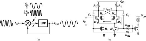
The Miller divider can achieve high speeds for two reasons: (1) the low-pass behavior can simply be due to the intrinsic time constant at the output node of the mixer, and (2) the circuit does not rely on latching and hence fails more gradually than flipflops as the input frequency increases. Note, however, that the divider loop requires some cycles to reach steady state, i.e., it does not divide correctly instantaneously.
Figure 10.61(b) shows an example of the Miller divider realization. A double-balanced mixer senses the input at its LO port, with C1 and C2 returning the output to the RF port.10 The loop gain at mid-band frequencies is equal to (2/π)gm1,2RD (Chapter 6) and must remain above unity. The maximum speed of the circuit is roughly given by the frequency at which the loop gain falls to unity. Note that RD and the total capacitance at the output nodes define the corner of the LPF. Of course, at high frequencies, the roll-off due to the pole at the drains of M1 and M2 may also limit the speed.

The reader may wonder why we said above that the component at 3fin/2 must be sufficiently small. After all, this component is merely the third harmonic of the desired output and would seem to only sharpen the output edges. However, this harmonic in fact creates a finite lower bound on the divider operation frequency. As fin decreases and the component at 3fin/2 falls below the corner frequency of the LPF, the circuit fails to divide.
To understand this point, let us open the loop as shown in Fig. 10.63(a) and write the output of the mixer as
where α is related to the mixer conversion gain. Illustrated in Fig. 10.63(b), this sum exhibits additional zero crossings, prohibiting frequency division if traveling through the LPF unchanged [14]. Thus, the third harmonic must be attenuated—at least by a factor of three [14]—to avoid the additional zero crossings.
Figure 10.63 (a) Open-loop equivalent circuit of Miller divider, (b) circuit’s waveforms.

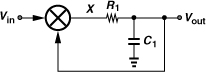
To avoid the additional zero crossings shown in Fig. 10.63(b), it is also possible to introduce phase shift in cos(ωint/2) and/or cos(3ωint/2). For example, if cos(3ωint/2) is attenuated by a factor of 2 but shifted by 45°, then the two components add up to the waveform shown in Fig. 10.65. In other words, the Miller divider operates properly if the third harmonic is attenuated and shifted so as to avoid the additional zero crossings [14]. This observation suggests that the topology of Fig. 10.61(b) divides successfully only if the pole at the drains of M1 and M2 provides enough phase shift, a difficult condition.
Figure 10.65 Proper Miller divider operation if third harmonic is shifted by 45° and halved in amplitude.
Miller Divider with Inductive Load
The topology of Fig. 10.61(b) suffers from the same gain-headroom trade-offs as those described for active mixers in Chapter 6. The limited voltage drop across the load resistors makes it difficult to achieve a high conversion gain. Wider input and LO transistors alleviate this issue but at the cost of speed. If the load resistors are replaced with inductors, the gain-headroom and gain-speed trade-offs are greatly relaxed, but the lower end of the frequency range rises. Also, the inductor complicates the layout. Figure 10.66 shows a Miller divider using inductive loads. Since the tanks significantly suppress the third harmonic of the desired output, this circuit proves more robust than the topology of Fig. 10.61(b) [14].
Figure 10.66 Miller divider using inductive loads.

The design of this circuit proceeds as follows. We assume a certain tolerable capacitance at the LO port and a certain load capacitance at the output node. The width of M3-M6 is chosen according to the former, and the LO common-mode level is preferably chosen equal to VDD, leaving maximum headroom for M1 and M2. Inductors L1 and L2 must resonate with the total capacitance at X and Y at about half of the input “mid-band” frequency. For example, if we wish to accommodate an input range of 40 GHz to 50 GHz, we may choose a resonance frequency around 22.5 GHz. In this step, the capacitance of M1 and M2 is unknown, requiring a reasonable guess and possible iterations. With the value of L1 and L2 known, their equivalent parallel resistance, Rp, must provide enough gain along with M1 and M2. [Recall that the mixer has a conversion gain of (2/π)gm1,2Rp.] The width and bias current of M1 and M2 are therefore chosen so as to maximize the gain. Of course, an excessively high bias current results in a low value for VP and VQ, driving M1 and M2 into the triode region. Some optimization is thus necessary. It can be shown that the input frequency range across which the circuit operates properly is given by
![]()
where ω0 and Q denote the tank resonance frequency and quality factor, respectively [14].
Solution:
Figure 10.67 (a) Inductively-loaded Miller divider with feedback to the switching quad, (b) alternative drawing of the circuit.

It is possible to construct a Miller divider using passive mixers. Figure 10.68 depicts an example, where M1-M4 constitute a passive mixer and M5-M6 an amplifier [16]. Since the output CM level is near VDD, the feedback path incorporates capacitive coupling, allowing the sources and drains of M1-M4 to remain about 0.4 V above ground. (As explained in Chapter 6, the LO CM level must still be near VDD to provide sufficient overdrive for M1-M4.) The cross-coupled pair M7-M8 can be added to increase the gain by virtue of its negative resistance. If excessively strong, however, this pair oscillates with the tanks, leading to a narrow frequency range (Section 10.6.6).
Figure 10.68 Miller divider using passive mixer.

While achieving speeds exceeding 100 GHz in CMOS technology [16], the Miller divider does not provide quadrature outputs, a drawback with respect to RF transceivers that operate the oscillator at twice the carrier frequency and employ a divider to generate the I and Q phases.
Miller Divider with Other Moduli
In his original paper, Miller also contemplates the use of dividers within the feedback loop of his topology so as to produce moduli other than 2. Shown in Fig. 10.69 is an example, where a ÷N circuit in the feedback path creates fb = fout/N, yielding fin ± fout/N at X. If the sum is suppressed by the LPF, then fout = fin − fout/N and hence
![]()
Figure 10.69 Miller divider having another divider stage in feedback.
Also,
![]()
For example, if N = 2, the input frequency is divided by 1.5 and 3, two moduli that are difficult to obtain at high speeds by means of flipflop-based dividers.
An important issue in the topology of Fig. 10.69 is that the sum component at X comes closer to the difference component as N increases, dictating a sharper LPF roll-off. In the above example, these two components lie at 4fin/3 and 2fin/3, respectively, i.e., only one octave apart. Consequently, the circuit suffers from a more limited frequency range.
Another critical issue in the Miller divider of Fig. 10.69 relates to the port-to-port feedthroughs of the mixer. The following example illustrates this point.
Solution:
Figure 10.70 (a) Miller divider with a ÷2 stage in feedback, (b) output spectrum, (c) spectrum at Y.
Does the original topology of Fig. 10.61(a) also suffer from spurs? In Problem 10.17, we prove that it does not.
The Miller divider frequency range can be extended through the use of a single-sideband mixer. Illustrated in Fig. 10.71(a), the idea is to suppress the sum component by SSB mixing rather than filtering, thereby avoiding the problem of additional zero crossings depicted in Fig. 10.63. In the absence of the sum component, the circuit divides properly at arbitrarily low frequencies. Unfortunately, however, this approach requires a broadband 90° phase shift, a very difficult design.
Figure 10.71 (a) Miller divider using SSB mixer, (b) divide-by-3 realization.
Nonetheless, the use of SSB mixing does prove useful if the loop contains a divider that generates quadrature outputs [17]. Shown in Fig. 10.71(b) is an example employing a ÷2 circuit and generating fin/3 at the output [17]. This topology achieves a wide frequency range and generates quadrature outputs, a useful property for multiband applications. By contrast, the flipflop-based ÷3 circuit in Fig. 10.28 does not provide quadrature outputs. We note from Example 10.28 that the ÷1.5 output available at X exhibits spurs and may not be suited to stringent systems.
The principal drawback of the circuit of Fig. 10.71(b) and its variants is that it requires quadrature LO phases. As explained in Chapter 8, quadrature oscillators exhibit a higher phase noise and two possible modes.
10.6.6 Injection-Locked Dividers
Another class of dividers is based on oscillators that are injection-locked to a harmonic of their oscillation frequency [15]. To understand this principle, let us return to the Miller divider of Fig. 10.68 and assume the cross-coupled pair is strong enough to produce oscillation. Transistors M5 and M6 can now be viewed as devices that couple the mixer output to the oscillator.11 The overall loop can thus be modeled as shown in Fig. 10.72, where the connection between X and the oscillator denotes injection rather than frequency control. If the loop operates properly, then fout = fin/2, yielding both fin/2 and 3fin/2 at X. The former couples to and locks the oscillator while the latter is suppressed by the selectivity of the oscillator. If fin varies across a certain “lock range,” the oscillator remains injection-locked to the fout − fin component at node X. On the other hand, if fin falls outside the lock range, the oscillator is injection-pulled, thus producing a corrupted output.
Figure 10.72 Injection-locked divider.

The reader may wonder if the injection-locked divider (ILD) of Fig. 10.72 is any different from the Miller loop of Fig. 10.61(a). The fundamental difference between the two is that the former oscillates even with the input amplitude set to zero, whereas the latter does not. For this reason, ILDs generally exhibit a narrower operation frequency range than Miller dividers.
Let us now implement an ILD. While the topology of Fig. 10.72 serves as a candidate, even a simpler arrangement is conceived if we recognize that the cross-coupled pair within an oscillator can also operate as a mixer. Indeed, we utilized this property to study the effect of the tail noise current on the phase noise in Chapter 8. The loop shown in Fig. 10.72 thus reduces to a single cross-coupled pair providing a negative resistance at its drains and a mixing input at its tail node. Figure 10.74(a) depicts the result: Iin (= gm3Vin) is commutated by M1 and M2 and hence translated to fout ± fin as it emerges at the drains of these transistors. The circuit can be equivalently viewed as shown in Fig. 10.74(b), where Ieq represents the current components at fout ± fin, with the amplitude of each component given by 2/π times the amplitude of Iin.12
Figure 10.74 (a) Example of injection-locked divider, (b) equivalent view.
Since the sum component is greatly attenuated by the oscillator, we can consider only the difference component as the input to the oscillator. From Chapter 8, the two-sided injection lock range is given by (ω0/Q)(Iinj/Iosc), where Iinj = (2/π)Iin. Thus, the output frequency range across which the circuit remains locked is given by [18]
![]()
The input lock range is twice this value:
![]()
As explained in Chapter 8, the phase noise of an injection-locked oscillator approaches that of the unlocked circuit if the oscillator is locked near the edge of the lock range. Equation (10.74) therefore points to a trade-off between the lock range and the phase noise: as Q is lowered, the former widens but the latter degrades.
As mentioned in Section 10.6.4, flipflop-based dividers can also be considered injection-locked ring oscillators. Achieving a much wider lock range than their LC oscillator counterparts, these dividers exhibit a low phase noise by virtue of strong locking to the input. It is important to bear in mind that LC oscillators exhibit injection-locking dynamics that require a settling time commensurate with their Q. That is, such dividers do not begin to operate correctly instantaneously.
It is also critical to note that, in a PLL environment, the divider lock range must exceed the VCO tuning range. During the lock transient, the VCO frequency swings up or down and, if the divider fails at any VCO frequency, the PLL may simply not lock.
10.6.7 Divider Delay and Phase Noise
A divider incorporating asynchronous logic may experience a significant delay from the input to the output. For example, in the pulse swallow divider of Fig. 10.24, all three counters contribute delay: on one edge of the main input, the prescaler incurs some delay before it produces a transition at node A, which must then propagate through the program counter to reach the output.
What is the effect of divider delay on an integer-N synthesizer? The transfer function of a stage having a constant delay of ΔT is given by exp(−ΔT · s), yielding an overall open-loop transfer function of
![]()
If the delay is small with respect to the time scales of interest, we can write exp(−ΔT · s) ≈ 1 − ΔT · s, recognizing that the delay results in a zero in the right-half plane. Such a zero contributes negative phase shift, −tan−1(ΔT · ω), making the loop less stable. Plotted in Fig. 10.75 is the open-loop frequency response in this case, revealing that the zero has two undesirable effects: it flattens the gain, pushing the gain crossover frequency to higher values (in principle, infinity), and it bends the phase profile downward. Thus, this zero must remain well above the original unity-gain bandwidth of the loop, e.g.,

Figure 10.75 Effect of divider delay on PLL phase margin.
In most practical designs, the divider delay satisfies the above condition, thus negligibly affecting the loop dynamics. Otherwise, the divider must employ more synchronous logic to reduce the delay.
The divider phase noise may also prove troublesome. As shown in Fig. 10.76, the output phase noise of the divider, φn,div, directly adds to the input phase noise, φn,in, experiencing the same low-pass response as it propagates to φout. In other words, φn,div is also multiplied by a factor of N within the loop bandwidth. Thus, for the divider to contribute negligible phase noise, we must have
![]()
Figure 10.76 Effect of divider phase noise on PLL.
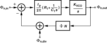
In narrowband synthesizers, of course, the output phase noise is dominated by that of the VCO, making φn,in and φn,div less critical. Nonetheless, if the divider phase noise is significant, a retiming flipflop can be used to suppress its effect. Illustrated in Fig. 10.77(a), the idea is to sample the divider output by the VCO waveform, thus presenting the edges to the PFD only at the VCO transitions. As depicted in Fig. 10.77(b), VY changes only when the VCO output changes, avoiding the jitter (phase noise) in VX (if the jitter is less than one cycle of Vout). In essence, the retiming operation bypasses the phase noise accumulated in the divider chain.
Figure 10.77 (a) Use of retiming FF to remove divider phase noise, (b) waveforms showing retiming operation, (c) problem of metastability.
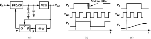
A concern in the use of the retiming FF in Fig. 10.77(a) arises if the VCO output edge occurs close to the transition at node X. Under this condition, the FF becomes “metastable,” i.e., it takes a long time to produce a well-defined logical level. Depicted in Fig. 10.77(c), this effect results in a distorted transition at node Y, confusing the PFD. It is therefore essential to guarantee by design that the sampling edges of the VCO remain safely away from the transitions at node X. If the divider delay varies by as much as one VCO period with process and temperature, then it becomes extremely difficult to avoid metastability.
References
[1] S. E. Meninger and M. H. Perrott, “A 1-MHz Bandwidth 3.6-GHz 0.18-μm CMOS Fractional-N Synthesizer Utilizing a Hybrid PFD/DAC Structure for Reduced Broadband Phase Noise,” IEEE J. Solid-State Circuits, vol. 41, pp. 966–981, April 2006.
[2] K. J. Wang, A. Swaminathan, and I. Galton, “Spurious Tone Suppression Techniques Applied to a Wide-Bandwidth 2.4 GHz Fractional-N PLL,” IEEE J. of Solid-State Circuits, vol. 43, pp. 2787–2797, Dec. 2008.
[3] A. Zolfaghari, A. Y. Chan, and B. Razavi, “A 2.4-GHz 34-mW CMOS Transceiver for Frequency-Hopping and Direct-Sequence Applications,” ISSCC Dig. Tech. Papers, pp. 418–419, Feb. 2001.
[4] G. Irvine et al., “An Upconversion Loop Transmitter IC for Digital Mobile Telephones,” ISSCC Dig. Tech. Papers, pp. 364–365, Feb. 1998.
[5] T. Yamawaki et al., “A 2.7-V GSM RF Transceiver IC,” IEEE J. of Solid-State Circuits, vol. 32, pp. 2089–2096, Dec. 1997.
[6] C. Lam and B. Razavi, “A 2.6-GHz/5.2-GHz Frequency Synthesizer in 0.4-μm CMOS Technology,” IEEE J. of Solid-State Circuits, vol. 35, pp. 788–794, May 2000.
[7] C. S. Vaucher et al., “A Family of Low-Power Truly Modular Programmable Dividers in Standard 0.35-μm CMOS Technology,” IEEE J. of Solid-State Circuits, vol. 35, pp. 1039–1045, July 2000.
[8] B. Razavi, Y. Ota, and R. G. Swartz, “Design Techniques for Low-Voltage High-Speed Digital Bipolar Circuits,” IEEE J. of Solid-State Circuits, vol. 29, pp. 332–339, March 1994.
[9] J. Lee and B. Razavi, “A 40-Gb/s Clock and Data Recovery Circuit in 0.18-μm CMOS Technology,” IEEE J. of Solid-State Circuits, vol. 38, pp. 2181–2190, Dec. 2003.
[10] D. D. Kim, K. Kim, and C. Cho, “A 94GHz Locking Hysteresis-Assisted and Tunable CML Static Divider in 65nm SOI CMOS,” ISSCC Dig. Tech. Papers, pp. 460–461, Feb. 2008.
[11] J. Yuan and C. Svensson, “High-Speed CMOS Circuit Technique,” IEEE J. Solid-State Circuits, vol. 24, pp. 62–70, Feb. 1989.
[12] B. Chang, J. Park, and W. Kim, “A 1.2-GHz CMOS Dual-Modulus Prescaler Using New Dynamic D-Type Flip-Flops,” IEEE J. Solid-State Circuits, vol. 31, pp. 749–754, May 1996.
[13] R. L. Miller, “Fractional-Frequency Generators Utilizing Regenerative Modulation,” Proc. IRE, vol. 27, pp. 446–456, July 1939.
[14] J. Lee and B. Razavi, “A 40-GHz Frequency Divider in 0.18-μm CMOS Technology,” IEEE J. of Solid-State Circuits, vol. 39, pp. 594–601, Apr. 2004.
[15] H. R. Rategh and T. H. Lee, “Superharmonic Injection-Locked Frequency Dividers,” IEEE J. of Solid-State Circuits, vol. 34, pp. 813–821, June 1999.
[16] B. Razavi, “A Millimeter-Wave CMOS Heterodyne Receiver with On-Chip LO and Divider,” IEEE J. of Solid-State Circuits, vol. 43, pp. 477–485, Feb. 2008.
[17] C.-C. Lin and C.-K. Wang, “A Regenerative Semi-Dynamic Frequency Divider for Mode-1 MB-OFDM UWB Hopping Carrier Generation,” ISSCC Dig. Tech. Papers, pp. 206–207, Feb. 2005.
[18] B. Razavi, “A Study of Injection Locking and Pulling in Oscillators,” IEEE J. of Solid-State Circuits, vol. 39, pp. 1415–1424, Sep. 2004.
Problems
10.1. Prove that insertion of a feedback divider in Fig. 10.14(b) results in Eqs. (10.25) and (10.26).
10.2. Prove that the far-out phase noise of the LO in Fig. 10.20 also appears as noise in the RX band. Neglecting other sources of noise, determine the phase noise at 25-MHz offset for GSM.
10.3. Does the sampling filter shown in Fig. 10.13(b) remove the effect of the mismatch between the Up and Down currents?
10.4. In practice, the sampling filter of Fig. 10.13(b) employs another capacitor tied from Vcont to ground. Explain why. How should this capacitor and C2 be chosen to negligibly degrade the loop stability?
10.5. Suppose S1 in Fig. 10.13(b) has a large on-resistance. Does this affect the loop stability?
10.6. Explain whether or not the charge injection and clock feedthrough of S1 in Fig. 10.13(b) produce ripple on the control voltage after the loop has locked.
10.7. An in-loop modulation scheme is shown in Fig. 10.78. Consider two cases: the baseband bit period is (I) much shorter, or (II) much longer than the loop time constant.
(a) Sketch the output waveform of the VCO for both cases.
(b) Sketch the output waveform of the divider for both cases.
Figure 10.78 PLL with in-loop modulation.
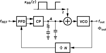
10.8. In the pulse swallow divider of Fig. 10.24, the modulus control of the prescaler is accidentally inverted. Explain what happens.
10.9. In the PLL shown in Fig. 10.79, the control voltage has a sinusoidal ripple at a frequency of fREF. Plot the spectra at A and B.
Figure 10.79 PLL with divide-by-two circuit preceding the dual-modulus divider.
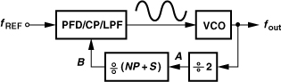
10.10. In the divider of Fig. 10.31, gate G1 is mistakenly realized as a NAND gate. Explain what happens.
10.11. How can the XOR of Fig. 10.42 be modified to provide differential outputs?
10.12. In the circuit of Fig. 10.44(a), the resistors are replaced with ideal current sources. Explain what happens.
10.13. In our study of oscillators in Chapter 8, we concluded that a loop containing only two poles cannot oscillate (unless both are at the origin). Why then does the circuit of Fig. 10.49 oscillate?
10.14. Example 10.18 suggests that τreg is independent of RD if gm3,4RD ![]() 1. Explain this property intuitively.
1. Explain this property intuitively.
10.15. Must the clock transition be abrupt for the D latch of Fig. 10.43(a) to operate properly? Consider a clock transition time (a) on the order of the time constant at X and Y, and (b) much longer than this time constant.
10.16. For the Miller divider of Fig. 10.68, determine the loop gain. Assume the tanks in the drains of M1 and M2 can be replaced by a resistance of Rp at resonance. Neglect all transistor capacitances and assume the resistors tied to the gates of M5 and M6 are large.
10.17. Prove that the Miller divider of Fig. 10.61(a) does not exhibit spurs at the output even if the mixer suffers from port-to-port feedthroughs.
10.18. Repeat the above problem if the mixer suffers from nonlinearity at each port.
10.19. Study the spurious response of the Miller divider shown in Fig. 10.69 if the mixer exhibits (a) port-to-port feedthrough, or (b) port nonlinearity.
10.20. Of the active mixer topologies studied in Chapter 6, which ones are suited to the Miller divider of Fig. 10.61(a)?