Chapter 1. Introduction to RF and Wireless Technology
Compare two RF transceivers designed for cell phones:
“A 2.7-V GSM RF Transceiver IC” [1] (published in 1997)
“A Single-Chip 10-Band WCDMA/HSDPA 4-Band GSM/EDGE SAW-Less CMOS Receiver with DigRF 3G Interface and +90-dBm IIP2” [2] (published in 2009)
Why is the latter much more complex than the former? Does the latter have a higher performance or only greater functionality? Which one costs more? Which one consumes a higher power? What do all the acronyms GSM, WCDMA, HSDPA, EDGE, SAW, and IIP2 mean? Why do we care?
The field of RF communication has grown rapidly over the past two decades, reaching far into our lives and livelihood. Our cell phones serve as an encyclopedia, a shopping terminus, a GPS guide, a weather monitor, and a telephone—all thanks to their wireless communication devices. We can now measure a patient’s brain or heart activity and transmit the results wirelessly, allowing the patient to move around untethered. We use RF devices to track merchandise, pets, cattle, children, and convicts.
1.1 A Wireless World
Wireless communication has become almost as ubiquitous as electricity; our refrigerators and ovens may not have a wireless device at this time, but it is envisioned that our homes will eventually incorporate a wireless network that controls every device and appliance. High-speed wireless links will allow seamless connections among our laptops, digital cameras, camcorders, cell phones, printers, TVs, microwave ovens, etc. Today’s WiFi and Bluetooth connections are simple examples of such links.
How did wireless communication take over the world? A confluence of factors has contributed to this explosive growth. The principal reason for the popularity of wireless communication is the ever-decreasing cost of electronics. Today’s cell phones cost about the same as those a decade ago but they offer many more functions and features: many frequency bands and communication modes, WiFi, Bluetooth, GPS, computing, storage, a digital camera, and a user-friendly interface. This affordability finds its roots in integration, i.e., how much functionality can be placed on a single chip—or, rather, how few components are left off-chip. The integration, in turn, owes its steady rise to (1) the scaling of VLSI processes, particularly, CMOS technology, and (2) innovations in RF architectures, circuits, and devices.
Along with higher integration levels, the performance of RF circuits has also improved. For example, the power consumption necessary for a given function has decreased and the speed of RF circuits has increased. Figure 1.1 illustrates some of the trends in RF integrated circuits (ICs) and technology for the past two decades. The minimum feature size of CMOS technology has fallen from 0.5 μm to 40 nm, the transit frequency,1 fT, of NMOS devices has risen from about 12 GHz to several hundred gigahertz, and the speed of RF oscillators has gone from 1.2 GHz to 300 GHz. Also shown is the number of RF and wireless design papers presented at the International Solid-State Circuits Conference (ISSCC) each year, revealing the fast-growing activity in this field.
Figure 1.1 Trends in RF circuits and technology.

1.2 RF Design Is Challenging
Despite many decades of work on RF and microwave theory and two decades of research on RF ICs, the design and implementation of RF circuits and transceivers remain challenging. This is for three reasons. First, as shown in Fig. 1.2, RF design draws upon a multitude of disciplines, requiring a good understanding of fields that are seemingly irrelevant to integrated circuits. Most of these fields have been under study for more than half a century, presenting a massive body of knowledge to a person entering RF IC design. One objective of this book is to provide the necessary background from these disciplines without overwhelming the reader.
Figure 1.2 Various disciplines necessary in RF design.

Second, RF circuits and transceivers must deal with numerous trade-offs, summarized in the “RF design hexagon” of Fig. 1.3. For example, to lower the noise of a front-end amplifier, we must consume a greater power or sacrifice linearity. We will encounter these trade-offs throughout this book.

Third, the demand for higher performance, lower cost, and greater functionality continues to present new challenges. The early RF IC design work in the 1990s strove to integrate one transceiver—perhaps along with the digital baseband processor—on a single chip. Today’s efforts, on the other hand, aim to accommodate multiple transceivers operating in different frequency bands for different wireless standards (e.g., Bluetooth, WiFi, GPS, etc.). The two papers mentioned at the beginning of this chapter exemplify this trend. It is interesting to note that the silicon chip area of early single-transceiver systems was dominated by the digital baseband processor, allowing RF and analog designers some latitude in the choice of their circuit and device topologies. In today’s designs, however, the multiple transceivers tend to occupy a larger area than the baseband processor, requiring that RF and analog sections be designed with much care about their area consumption. For example, while on-chip spiral inductors (which have a large footprint) were utilized in abundance in older systems, they are now used only sparingly.
1.3 The Big Picture
The objective of an RF transceiver is to transmit and receive information. We envision that the transmitter (TX) somehow processes the voice or data signal and applies the result to the antenna [Fig. 1.4(a)]. Similarly, the receiver (RX) senses the signal picked up by the antenna and processes it so as to reconstruct the original voice or data information. Each black box in Fig. 1.4(a) contains a great many functions, but we can readily make two observations: (1) the TX must drive the antenna with a high power level so that the transmitted signal is strong enough to reach far distances, and (2) the RX may sense a small signal (e.g., when a cell phone is used in the basement of a building) and must first amplify the signal with low noise. We now architect our transceiver as shown in Fig. 1.4(b), where the signal to be transmitted is first applied to a “modulator” or “upconverter” so that its center frequency goes from zero to, say, fc = 2.4 GHz. The result drives the antenna through a “power amplifier” (PA). On the receiver side, the signal is sensed by a “low-noise amplifier” (LNA) and subsequently by a “downconverter” or “demodulator” (also known as a “detector”).
Figure 1.4 (a) Simple view of RF communication, (b) more complete view, (c) generic RF transceiver.
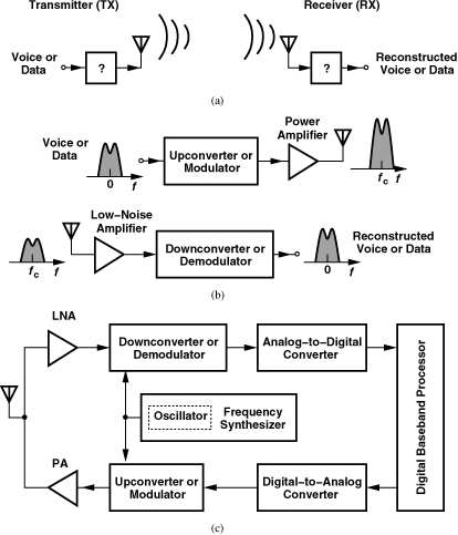
The upconversion and downconversion paths in Fig. 1.4(b) are driven by an oscillator, which itself is controlled by a “frequency synthesizer.” Figure 1.4(c) shows the overall transceiver.2 The system looks deceptively simple, but we will need the next 900 pages to cover its RF sections. And perhaps another 900 pages to cover the analog-to-digital and digital-to-analog converters.
References
[1] T. Yamawaki et al., “A 2.7-V GSM RF Transceiver IC,” IEEE J. Solid-State Circuits, vol. 32, pp. 2089–2096, Dec. 1997.
[2] D. Kaczman et al., “A Single-Chip 10-Band WCDMA/HSDPA 4-Band GSM/EDGE SAW-less CMOS Receiver with DigRF 3G Interface and +90-dBm IIP2,” IEEE J. Solid-State Circuits, vol. 44, pp. 718–739, March 2009.
[3] M. Banu, “MOS Oscillators with Multi-Decade Tuning Range and Gigahertz Maximum Speed,” IEEE J. Solid-State Circuits, vol. 23, pp. 474–479, April 1988.
[4] B. Razavi et al., “A 3-GHz 25-mW CMOS Phase-Locked Loop,” Dig. of Symposium on VLSI Circuits, pp. 131–132, June 1994.
[5] M. Soyuer et al., “A 3-V 4-GHz nMOS Voltage-Controlled Oscillator with Integrated Resonator,” IEEE J. Solid-State Circuits, vol. 31, pp. 2042–2045, Dec. 1996.
[6] B. Kleveland et al., “Monolithic CMOS Distributed Amplifier and Oscillator,” ISSCC Dig. Tech. Papers, pp. 70–71, Feb. 1999.
[7] H. Wang, “A 50-GHz VCO in 0.25-μm CMOS,” ISSCC Dig. Tech. Papers, pp. 372–373, Feb. 2001.
[8] L. Franca-Neto, R. Bishop, and B. Bloechel, “64 GHz and 100 GHz VCOs in 90 nm CMOS Using Optimum Pumping Method,” ISSCC Dig. Tech. Papers, pp. 444–445, Feb. 2004.
[9] E. Seok et al., “A 410GHz CMOS Push-Push Oscillator with an On-Chip Patch Antenna” ISSCC Dig. Tech. Papers, pp. 472–473, Feb. 2008.
[10] B. Razavi, “A 300-GHz Fundamental Oscillator in 65-nm CMOS Technology,” Symposium on VLSI Circuits Dig. Of Tech. Papers, pp. 113–114, June 2010.