
Chapter 5. Low-Noise Amplifiers
Following our system- and architecture-level studies in previous chapters, we move farther down to the circuit level in this and subsequent chapters. Beginning with the receive path, we describe the design of low-noise amplifiers. While our focus is on CMOS implementations, most of the concepts can be applied to other technologies as well. The outline of the chapter is shown below.
5.1 General Considerations
As the first active stage of receivers, LNAs play a critical role in the overall performance and their design is governed by the following parameters.
Noise Figure
The noise figure of the LNA directly adds to that of the receiver. For a typical RX noise figure of 6 to 8 dB, it is expected that the antenna switch or duplexer contributes about 0.5 to 1.5 dB, the LNA about 2 to 3 dB, and the remainder of the chain about 2.5 to 3.5 dB. While these values provide a good starting point in the receiver design, the exact partitioning of the noise is flexible and depends on the performance of each stage in the chain. In modern RF electronics, we rarely design an LNA in isolation. Rather, we view and design the RF chain as one entity, performing many iterations among the stages.
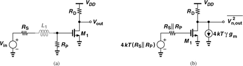
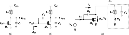
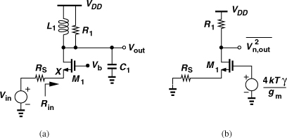
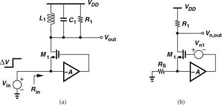
To gain a better feel for a noise figure of 2 dB, consider the simple example in Fig. 5.1(a), where the noise of the LNA is represented by only a voltage source. Rearranging the input network as shown in Fig. 5.1(b), we have from Chapter 2

Figure 5.1 (a) LNA with input-referred noise voltage, (b) simplified circuit.

Thus, a noise figure of 2 dB with respect to a source impedance of 50Ω translates to ![]() , an extremely low value. For the gate-referred thermal noise voltage of a MOSFET, 4kTγ/gm, to reach this value, the gm must be as high as (29Ω)−1 (if γ = 1). In this chapter, we assume RS = 50Ω.
, an extremely low value. For the gate-referred thermal noise voltage of a MOSFET, 4kTγ/gm, to reach this value, the gm must be as high as (29Ω)−1 (if γ = 1). In this chapter, we assume RS = 50Ω.
A student lays out an LNA and connects its input to a pad through a metal line 200 μm long. In order to minimize the input capacitance, the student chooses a width of 0.5 μm for the line. Assuming a noise figure of 2 dB for the LNA and a sheet resistance of 40 mΩ/![]() for the metal line, determine the overall noise figure. Neglect the input-referred noise current of the LNA.
for the metal line, determine the overall noise figure. Neglect the input-referred noise current of the LNA.
Solution:
We draw the equivalent circuit as shown in Fig. 5.2, pretending that the line resistance, RL, is part of the LNA. The total input-referred noise voltage of the circuit inside the box is therefore equal to ![]() . We thus write
. We thus write

where NFLNA denotes the noise figure of the LNA without the line resistance. Since NFLNA = 2 dB ≡ 1.58 and RL = (200/0.5) × 40 mΩ/![]() = 16Ω, we have
= 16Ω, we have
![]()
Figure 5.2 LNA with metal resistance in series with its input.
The low noise required of LNAs limits the choice of the circuit topology. This often means that only one transistor—usually the input device—can be the dominant contributor to NF, thus ruling out configurations such as emitter or source followers.
Gain
The gain of the LNA must be large enough to minimize the noise contribution of subsequent stages, specifically, the downconversion mixer(s). As described in Chapter 2, the choice of this gain leads to a compromise between the noise figure and the linearity of the receiver as a higher gain makes the nonlinearity of the subsequent stages more pronounced. In modern RF design, the LNA directly drives the downconversion mixer(s) with no impedance matching between the two. Thus, it is more meaningful and simpler to perform the chain calculations in terms of the voltage gain—rather than power gain—of the LNA.
It is important to note that the noise and IP3 of the stage following the LNA are divided by different LNA gains. Consider the LNA/mixer cascade shown in Fig. 5.3(a), where the input-referred noise voltages are denoted by ![]() and
and ![]() and input noise currents are neglected. Assuming a unity voltage gain for the mixer for simplicity, we write the total output noise as
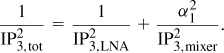
and input noise currents are neglected. Assuming a unity voltage gain for the mixer for simplicity, we write the total output noise as ![]() . The overall noise figure is thus equal to
. The overall noise figure is thus equal to

Figure 5.3 Appropriate choice of gain for referring (a) noise and (b) IP3 of a mixer to LNA input.
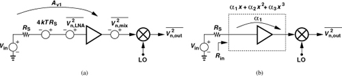
In other words, for NF calculations, the noise of the second stage is divided by the gain from the input voltage source to the LNA output.
Now consider the same cascade repeated in Fig. 5.3(b) with the nonlinearity of the LNA expressed as a third-order polynomial. From Chapter 2, we have1
In this case, α1 denotes the voltage gain from the input of the LNA to its output. With input matching, we have Rin = RS and α1 = 2Av1. That is, the mixer noise is divided by the lower gain and the mixer IP3 by the higher gain—both against the designer’s wish.
Input Return Loss
The interface between the antenna and the LNA entails an interesting issue that divides analog designers and microwave engineers. Considering the LNA as a voltage amplifier, we may expect that its input impedance must ideally be infinite. From the noise point of view, we may precede the LNA with a transformation network to obtain minimum NF. From the signal power point of view, we may realize conjugate matching between the antenna and the LNA. Which one of these choices is preferable?
We make the following observations. (1) the (off-chip) band-select filter interposed between the antenna and the LNA is typically designed and characterized as a high-frequency device and with a standard termination of 50Ω. If the load impedance seen by the filter (i.e., the LNA input impedance) deviates from 50Ω significantly, then the pass-band and stopband characteristics of the filter may exhibit loss and ripple. (2) Even in the absence of such a filter, the antenna itself is designed for a certain real load impedance, suffering from uncharacterized loss if its load deviates from the desired real value or contains an imaginary component. Antenna/LNA co-design could improve the overall performance by allowing even non-conjugate matching, but it must be borne in mind that, if the antenna is shared with the transmitter, then its impedance must contain a negligible imaginary part so that it radiates the PA signal. (3) In practice, the antenna signal must travel a considerable distance on a printed-circuit board before reaching the receiver. Thus, poor matching at the RX input leads to significant reflections, an uncharacterized loss, and possibly voltage attenuation. For these reasons, the LNA is designed for a 50-Ω resistive input impedance. Since none of the above concerns apply to the other interfaces within the RX (e.g., between the LNA and the mixer or between the LO and the mixer), they are typically designed to maximize voltage swings rather than power transfer.
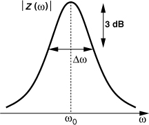
The quality of the input match is expressed by the input “return loss,” defined as the reflected power divided by the incident power. For a source impedance of RS, the return loss is given by2

where Zin denotes the input impedance. An input return loss of −10 dB signifies that one-tenth of the power is reflected—a typically acceptable value. Figure 5.4 plots contours of constant Γ in the Zin plane. Each contour is a circle with its center shown. For example, Re{Zin} = 1.22 × 50Ω = 61Ω and Im{Zin} = 0.703 × 50Ω = 35.2Ω yield S11 = −10 dB. In Problem 5.1, we derive the equations for these contours. We should remark that, in practice, a Γ of about −15 dB is targeted so as to allow margin for package parasitics, etc.
Figure 5.4 Constant-Γ contours in the input impedance plane.

Stability
Unlike the other circuits in a receiver, the LNA must interface with the “outside world,” specifically, a poorly-controlled source impedance. For example, if the user of a cell phone wraps his/her hand around the antenna, the antenna impedance changes.3 For this reason, the LNA must remain stable for all source impedances at all frequencies. One may think that the LNA must operate properly only in the frequency band of interest and not necessarily at other frequencies, but if the LNA begins to oscillate at any frequency, it becomes highly nonlinear and its gain is very heavily compressed.
A parameter often used to characterize the stability of circuits is the “Stern stability factor,” defined as
![]()
where Δ = S11S22 − S12S21. If K > 1 and Δ < 1, then the circuit is unconditionally stable, i.e., it does not oscillate with any combination of source and load impedances. In modern RF design, on the other hand, the load impedance of the LNA (the input impedance of the on-chip mixer) is relatively well-controlled, making K a pessimistic measure of stability. Also, since the LNA output is typically not matched to the input of the mixer, S22 is not a meaningful quantity in such an environment.
The above example suggests that LNAs can be stabilized by maximizing their reverse isolation. As explained in Section 5.3, this point leads to two robust LNA topologies that are naturally stable and hence can be optimized for other aspects of their performance with no stability concerns. A high reverse isolation is also necessary for suppressing the LO leakage to the input of the LNA.
LNAs may become unstable due to ground and supply parasitic inductances resulting from the packaging (and, at frequencies of tens of gigahertz, the on-chip line inductances). For example, if the gate terminal of a common-gate transistor sees a large series inductance, the circuit may suffer from substantial feedback from the output to the input and become unstable at some frequency. For this reason, precautions in the design and layout as well as accurate package modeling are essential.
Linearity
In most applications, the LNA does not limit the linearity of the receiver. Owing to the cumulative gain through the RX chain, the latter stages, e.g., the baseband amplifiers or filters tend to limit the overall input IP3 or P1dB. We therefore design and optimize LNAs with little concern for their linearity.
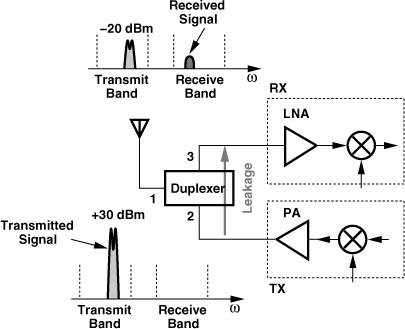
An exception to the above rule arises in “full-duplex” systems, i.e., applications that transmit and receive simultaneously (and hence incorporate FDD). Exemplified by the CDMA systems studied in Chapter 3, full-duplex operation must deal with the leakage of the strong transmitted signal to the receiver. To understand this issue, let us consider the front end shown in Fig. 5.5, where a duplexer separates the TX and RX bands. Modeling the duplexer as a three-port network, we note that S31 and S21 represent the losses in the RX and TX paths, respectively, and are about 1 to 2 dB. Unfortunately, leakages through the filter and the package yield a finite isolation between ports 2 and 3, as characterized by an S32 of about −50 dB. In other words, if the PA produces an average output power of +30 dBm (1 W), then the LNA experiences a signal level of −20 dBm in the TX band while sensing a much smaller received signal. Since the TX signal exhibits a variable envelope, its peak level may be about 2 dB higher. Thus, the receiver must remain uncompressed for an input level of −18 dBm. We must therefore choose a P1dB of about −15 dBm to allow some margin.
Figure 5.5 TX leakage to RX in a full-duplex system.
Such a value for P1dB may prove difficult to realize in a receiver. With an LNA gain of 15 to 20 dB, an input of −15 dBm yields an output of 0 to +5 dBm (632 to 1124 mVpp), possibly compressing the LNA at its output. The LNA linearity is therefore critical. Similarly, the 1-dB compression point of the downconversion mixer(s) must reach 0 to +5 dBm. (The corresponding mixer IP3 is roughly +10 to +15 dBm.) Thus, the mixer design also becomes challenging. For this reason, some CDMA receivers interpose an off-chip filter between the LNA and the mixer(s) so as to remove the TX leakage [1].
The linearity of the LNA also becomes critical in wideband receivers that may sense a large number of strong interferers. Examples include “ultra-wideband” (UBW), “software-defined,” and “cognitive” radios.
Bandwidth
The LNA must provide a relatively flat response for the frequency range of interest, preferably with less than 1 dB of gain variation. The LNA −3-dB bandwidth must therefore be substantially larger than the actual band so that the roll-off at the edges remains below 1 dB.
In order to quantify the difficulty in achieving the necessary bandwidth in a circuit, we often refer to its “fractional bandwidth,” defined as the total −3-dB bandwidth divided by the center frequency of the band. For example, an 802.11g LNA requires a fractional bandwidth greater than 80 MHz/2.44 GHz = 0.0328.
LNA designs that must achieve a relatively large fractional bandwidth may employ a mechanism to switch the center frequency of operation. Depicted in Fig. 5.7(a) is an example, where an additional capacitor, C2, can be switched into the tank, thereby changing the center frequency from ![]() to
to ![]() [Fig. 5.7(b)]. We return to this concept in Section 5.5.
[Fig. 5.7(b)]. We return to this concept in Section 5.5.
Figure 5.7 (a) Band switching, (b) resulting frequency response.

Power Dissipation
The LNA typically exhibits a direct trade-off among noise, linearity, and power dissipation. Nonetheless, in most receiver designs, the LNA consumes only a small fraction of the overall power. In other words, the circuit’s noise figure generally proves much more critical than its power dissipation.
5.2 Problem of Input Matching
As explained in Section 5.1, LNAs are typically designed to provide a 50-Ω input resistance and negligible input reactance. This requirement limits the choice of LNA topologies. In other words, we cannot begin with an arbitrary configuration, design it for a certain noise figure and gain, and then decide how to create input matching.
Let us first consider the simple common-source stage shown in Fig. 5.8, where CF represents the gate-drain overlap capacitance. At very low frequencies, RD is much smaller than the impedances of CF and CL and the input impedance is roughly equal to [(CGS + CF)s]−1. At very high frequencies, CF shorts the gate and drain terminals of M1, yielding an input resistance equal to RD||(1/gm). More generally, the reader can prove that the real and imaginary parts of the input admittance are, respectively, equal to
![]()
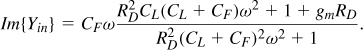
Figure 5.8 Input admittance of a CS stage.
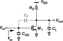
Is it possible to select the circuit parameters so as to obtain Re{Yin} = 1/(50Ω)? For example, if CF = 10 fF, CL = 30 fF, gmRD = 4, and RD = 100Ω, then Re{Yin} = (7.8 kΩ)−1 at 5 GHz, far from (50Ω)−1. This is because CF introduces little feedback at this frequency.
Can we employ simple resistive termination at the input? Illustrated in Fig. 5.9(a), such a topology is designed in three steps: (1) M1 and RD provide the required noise figure and gain, (2) RP is placed in parallel with the input to provide Re{Zin} = 50Ω, and (3) an inductor is interposed between RS and the input to cancel Im{Zin}. Unfortunately, as explained in Chapter 2, the termination resistor itself yields a noise figure of 1 + RS/RP. To calculate the noise figure at low frequencies, we can utilize Friis’ equation4 or simply treat the entire LNA as one circuit and, from Fig. 5.9(b), express the total output noise as
![]()
where channel-length modulation is neglected. Since the voltage gain from Vin to Vout in Fig. 5.9(a) is equal to −[RP/(RP + RS)]gmRD, the noise figure is given by
![]()
Figure 5.9 (a) Use of resistive termination for matching, (b) simplified circuit.
For RP ≈ RS, the NF exceeds 3 dB—perhaps substantially.
The key point in the foregoing study is that the LNA must provide a 50-Ω input resistance without the thermal noise of a physical 50-Ω resistor. This becomes possible with the aid of active devices.
Figure 5.10 (a) Use of matching circuit to transform the value of RP, (b) general representation of (a), (c) inclusion of noise of RP, (d) simplified circuit of (c), (e) simplified circuit of (d).

Solution:
![]()
![]()
Let us now compute the output noise with the aid of Fig. 5.10(c). The output noise due to the noise of RS is readily obtained from Eq. (5.19) by the substitution ![]() :
:
![]()
![]()
![]()
![]()
In summary, proper input (conjugate) matching of LNAs requires certain circuit techniques that yield a real part of 50Ω in the input impedance without the noise of a 50-Ω resistor. We study such techniques in the next section.
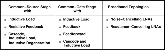
5.3 LNA Topologies
Our preliminary studies thus far suggest that the noise figure, input matching, and gain constitute the principal targets in LNA design. In this section, we present a number of LNA topologies and analyze their behavior with respect to these targets. Table 5.1 provides an overview of these topologies.
Table 5.1 Overview of LNA topologies.
5.3.1 Common-Source Stage with Inductive Load
As noted in Section 5.1, a CS stage with resistive load (Fig. 5.8) proves inadequate because it does not provide proper matching. Furthermore, the output node time constant may prohibit operation at high frequencies. In general, the trade-off between the voltage gain and the supply voltage in this circuit makes it less attractive as the latter scales down with technology. For example, at low frequencies,
where VRD denotes the dc voltage drop across RD and is limited by VDD. With channel-length modulation, the gain is even lower.
In order to circumvent the trade-off expressed by Eq. (5.29) and also operate at higher frequencies, the CS stage can incorporate an inductive load. Illustrated in Fig. 5.11(a), such a topology operates with very low supply voltages because the inductor sustains a smaller dc voltage drop than a resistor does. (For an ideal inductor, the dc drop is zero.) Moreover, L1 resonates with the total capacitance at the output node, affording a much higher operation frequency than does the resistively-loaded counterpart of Fig. 5.8.
Figure 5.11 (a) Inductively-loaded CS stage, (b) input impedance in the presence of CF, (c) equivalent circuit.
How about the input matching? We consider the more complete circuit shown in Fig. 5.11(b), where CF denotes the gate-drain overlap capacitance. Ignoring the gate-source capacitance of M1 for now, we wish to compute Zin. We redraw the circuit as depicted in Fig. 5.11(c) and note that the current flowing through the output parallel tank is equal to IX − gmVX. In this case, the inductor loss is modeled by a series resistance, RS, because this resistance varies much less with frequency than the equivalent parallel resistance does.5 The tank impedance is given by
![]()
and the tank voltage by (IX − gmVX)ZT. Adding the voltage drop across CF to the tank voltage, we have
![]()
Substitution of ZT from (5.30) gives
![]()
For s = jω,
![]()
Since the real part of a complex fraction (a + jb)/(c + jd) is equal to (ac + bd)/(c2 + d2), we have
![]()
where D is a positive quantity. It is thus possible to select the values so as to obtain Re{Zin} = 50Ω.
While providing the possibility of Re{Zin} = 50Ω at the frequency of interest, the feedback capacitance in Fig. 5.11(b) gives rise to a negative input resistance at other frequencies, potentially causing instability. To investigate this point, let us rewrite Eq. (5.34) as
![]()
We note that the numerator falls to zero at a frequency given by
![]()
Thus, at this frequency (if it exists), Re{Zin} changes sign. For example, if CF = 10fF, C1 = 30fF, gm = (20Ω)−1, L1 = 5 nH, and RS = 20Ω, then gmL1 dominates in the numerator, yielding ![]() and hence ω1 ≈ 2π × (11.3 GHz).
and hence ω1 ≈ 2π × (11.3 GHz).
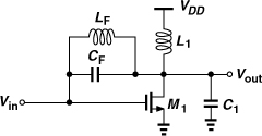
It is possible to “neutralize” the effect of CF in some frequency range through the use of parallel resonance (Fig. 5.12), but, since CF is relatively small, LF must assume a large value, thereby introducing significant parasitic capacitances at the input and output (and even between the input and output) and degrading the performance. For these reasons, this topology is rarely used in modern RF design.
Figure 5.12 Neutralization of CF by LF.
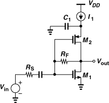
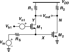
5.3.2 Common-Source Stage with Resistive Feedback
If the frequency of operation remains an order of magnitude lower than the fT of the transistor, the feedback CS stage depicted in Fig. 5.13(a) may be considered as a possible candidate. Here, M2 operates as a current source and RF senses the output voltage and returns a current to the input. We wish to design this stage for an input resistance equal to RS and a relatively low noise figure.
If channel-length modulation is neglected, we have from Fig. 5.13(b),
![]()
because RF is simply in series with an ideal current source and M1 appears as a diode-connected device. We must therefore choose
![]()
Figure 5.13 (a) CS stage with resistive feedback, (b) simplified circuit.
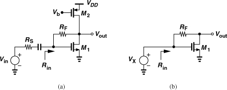
Figure 5.13(b) also implies that the small-signal drain current of M1, gm1VX, entirely flows through RF, generating a voltage drop of gm1VXRF. It follows that
![]()
and hence
In practice, RF ![]() RS, and the voltage gain from Vin to Vout in Fig. 5.13(a) is equal to
RS, and the voltage gain from Vin to Vout in Fig. 5.13(a) is equal to
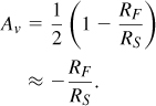
In contrast to the resistively-loaded CS stage of Fig. 5.8, this circuit does not suffer from a direct trade-off between gain and supply voltage because RF carries no bias current.
Let us determine the noise figure of the circuit, assuming that gm1 = 1/RS. We first compute the noise contributions of RF, M1, and M2 at the output. From Fig. 5.14(a), the reader can show the noise of RF appears at the output in its entirety:
![]()
Figure 5.14 Effect of noise of (a) RF and (b) M1 in CS stage.

The noise currents of M1 and M2 flow through the output impedance of the circuit, Rout, as shown in Fig. 5.14(b). The reader can prove that
![]()
The noise of RS is multiplied by the gain when referred to the output, and the result is divided by the gain when referred to the input. We thus have
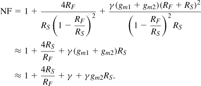
For γ ≈ 1, the NF exceeds 3 dB even if 4RS/RF + γgm2RS ![]() 1.
1.
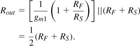
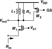
5.3.3 Common-Gate Stage
The low input impedance of the common-gate (CG) stage makes it attractive for LNA design. Since a resistively-loaded stage suffers from the same gain-headroom trade-off as its CS counterpart, we consider only a CG circuit with inductive loading [Fig. 5.16(a)]. Here, L1 resonates with the total capacitance at the output node (including the input capacitance of the following stage), and R1 represents the loss of L1. If channel-length modulation and body effect are neglected, Rin = 1/gm. Thus, the dimensions and bias current of M1 are chosen so as to yield gm = 1/RS = (50Ω)−1. The voltage gain from X to the output node at the output resonance frequency is then equal to

and hence Vout/Vin = R1/(2RS).
Figure 5.16 (a) CG stage, (b) effect of noise of M1.
Let us now determine the noise figure of the circuit under the condition gm = 1/RS and at the resonance frequency. Modeling the thermal noise of M1 as a voltage source in series with its gate, ![]() [Fig. 5.16(b)], and multiplying it by the gain from the gate of M1 to the output, we have
[Fig. 5.16(b)], and multiplying it by the gain from the gate of M1 to the output, we have
The output noise due to R1 is simply equal to 4kTR1. To obtain the noise figure, we divide the output noise due to M1 and R1 by the gain and 4kTRS and add unity to the result:
Even if 4RS/R1 ![]() 1 + γ, the NF still reaches 3 dB (with γ ≈ 1), a price paid for the condition gm = 1/RS. In other words, a higher gm yields a lower NF but also a lower input resistance. In Problem 5.8, we show that the NF can be lower if some impedance mismatch is permitted at the input.
1 + γ, the NF still reaches 3 dB (with γ ≈ 1), a price paid for the condition gm = 1/RS. In other words, a higher gm yields a lower NF but also a lower input resistance. In Problem 5.8, we show that the NF can be lower if some impedance mismatch is permitted at the input.
Figure 5.17 CG stage biasing with (a) current source and (b) resistor.
Solution:
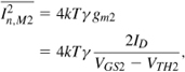
Figure 5.18 Proper biasing of CG stage.
In deep-submicron CMOS technologies, channel-length modulation significantly impacts the behavior of the CG stage. As shown in Fig. 5.19, the positive feedback through rO raises the input impedance. Since the drain-source current of M1 (without rO) is equal to −gmVX (if body effect is neglected), the current flowing through rO is given by IX − gmVX, yielding a voltage drop of rO(IX − gmVX) across it. Also, IX flows through the output tank, producing a voltage of IXR1 at the resonance frequency. Adding this voltage to the drop across rO and equating the result to VX, we obtain
![]()
Figure 5.19 Input impedance of CG stage in the presence of rO.
That is,
![]()
If the intrinsic gain, gmrO, is much greater than unity, then VX/IX ≈ 1/gm + R1/(gmrO). However, in today’s technology, gmrO hardly exceeds 10. Thus, the term R1/(gmrO) may become comparable with or even exceed the term 1/gm, yielding an input resistance substantially higher than 50Ω.
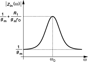
With the strong effect of R1 on Rin, we must equate the actual input resistance to RS to guarantee input matching:
![]()
The reader can prove that the voltage gain of the CG stage shown in Fig. 5.16(a) with a finite rO is expressed as
![]()
which, from Eq. (5.65), reduces to
This is a disturbing result! If rO and R1 are comparable, then the voltage gain is on the order of gmrO/4, a very low value.
In summary, the input impedance of the CG stage is too low if channel-length modulation is neglected and too high if it is not! A number of circuit techniques have been introduced to deal with the former case (Section 5.3.5), but in today’s technology, we face the latter case.
In order to alleviate the above issue, the channel length of the transistor can be increased, thus reducing channel-length modulation and raising the achievable gmrO. Since the device width must also increase proportionally so as to retain the transconductance value, the gate-source capacitance of the transistor rises considerably, degrading the input return loss.
Cascode CG Stage
An alternative approach to lowering the input impedance is to incorporate a cascode device as shown in Fig. 5.21. Here, the resistance seen looking into the source of M2 is given by Eq. (5.64):
![]()

This load resistance is now transformed to a lower value by M1, again according to (5.64):
![]()
If gmrO ![]() 1, then
1, then
![]()
Since R1 is divided by the product of two intrinsic gains, its effect remains negligible. Similarly, the third term is much less than the first if gm1 and gm2 are roughly equal. Thus, Rin ≈ 1/gm1.
The addition of the cascode device entails two issues: the noise contribution of M2 and the voltage headroom limitation due to stacking two transistors. To quantify the former, we consider the equivalent circuit shown in Fig. 5.22(a), where RS ( = 1/gm1) and M1 are replaced with an output resistance equal to 2rO1 (why?), and CX = CDB1 + CGD1 + CSB2. For simplicity, we have also replaced the tank with a resistor R1, i.e., the output node has a broad bandwidth. Neglecting the gate-source capacitance, channel-length modulation, and body effect of M2, we express the transfer function from Vn2 to the output at the resonance frequency as
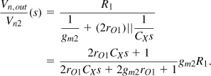
Figure 5.22 (a) Cascode transistor noise, (b) output contribution as a function of frequency.
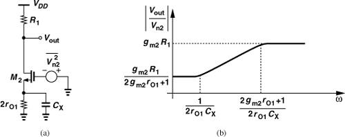
Figure 5.22(b) plots the frequency response, implying that the noise contribution of M2 is negligible for frequencies up to the zero frequency, (2rO1CX)−1, but begins to manifest itself thereafter. Since CX is comparable with CGS and 2rO1 ![]() 1/gm, we note that (2rO1CX)−1
1/gm, we note that (2rO1CX)−1 ![]() gm/CGS (≈ ωT). That is, the zero frequency is much lower than the fT of the transistors, making this effect potentially significant.
gm/CGS (≈ ωT). That is, the zero frequency is much lower than the fT of the transistors, making this effect potentially significant.
Assuming 2rO1 ![]() |CXs|−1 at frequencies of interest so that the degeneration impedance in the source of M2 reduces to CX, recompute the above transfer function while taking CGS2 into account. Neglect the effect of rO2.
|CXs|−1 at frequencies of interest so that the degeneration impedance in the source of M2 reduces to CX, recompute the above transfer function while taking CGS2 into account. Neglect the effect of rO2.
Solution:
![]()
Figure 5.23 Computation of gain from the gate of cascode device to output.

![]()
At frequencies well below the fT of the transistor, |(CGS2 + CX)s| ![]() gm2 and
gm2 and
![]()
The second issue stemming from the cascode device relates to the limited voltage headroom. To quantify this limitation, let us determine the required or allowable values of Vb1 and Vb2 in Fig. 5.21. Since the drain voltage of M2 begins at VDD and can swing below its gate voltage by as much as VTH2 while keeping M2 in saturation, we can simply choose Vb2 = VDD. Now, VX = VDD − VGS2, allowing a maximum value of VDD − VGS2 + VTH1 for Vb1 if M1 must remain saturated. Consequently, the source voltage of M1 cannot exceed VDD − VGS2 − (VGS1 − VTH1). We say the two transistors consume a voltage headroom of one VGS plus one overdrive (VGS1 − VTH1).
It may appear that, so long as VDD > VGS2 + (VGS1 − VTH1), the circuit can be properly biased, but how about the path from the source of M1 to ground? In comparison with the CG stages in Fig. 5.17, the cascode topology consumes an additional voltage headroom of VGS1 − VTH1, leaving less for the biasing transistor or resistor and hence raising their noise contribution. For example, suppose ID1 = ID2 = 2 mA. Since gm1 = (50Ω)−1 = 2ID/(VGS1 − VTH1), we have VGS1 − VTH1 = 200 mV. Also assume VGS2 ≈ 500 mV. Thus, with VDD = 1 V, the voltage available for a bias resistor, RB, tied between the source of M1 and ground cannot exceed 300 mV/2mA = 150Ω. This value is comparable with RS = 50Ω and degrades the gain and noise behavior of the circuit considerably.
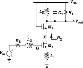
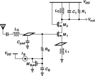
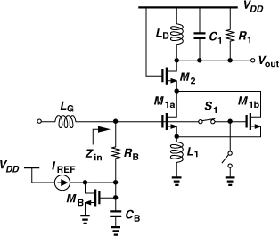
In order to avoid the noise-headroom trade-off imposed by RB, and also cancel the input capacitance of the circuit, CG stages often employ an inductor for the bias path. Illustrated in Fig. 5.24 with proper biasing for the input transistor, this technique minimizes the additional noise due to the biasing element (LB) and significantly improves the input matching. In modern RF design, both LB and L1 are integrated on the chip.
Figure 5.24 Biasing of cascode CG stage.

Design Procedure
With so many devices present in the circuit of Fig. 5.24, how do we begin the design? We describe a systematic procedure that provides a “first-order” design, which can then be refined and optimized.
The design procedure begins with two knowns: the frequency of operation and the supply voltage. In the first step, the dimensions and bias current of M1 must be chosen such that a transconductance of (50Ω)−1 is obtained. The length of the transistor is set to the minimum allowable by the technology, but how should the width and the drain current be determined?
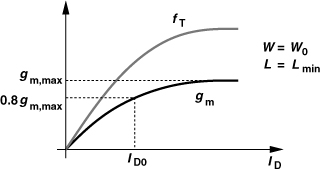
Using circuit simulations, we plot the transconductance and fT of an NMOS transistor with a given width, W0, as a function of the drain current. For long-channel devices, ![]() , but submicron transistors suffer from degradation of the mobility with the vertical field in the channel, exhibiting the saturation behavior shown in Fig. 5.25. To avoid excessive power consumption, we select a bias current, ID0, that provides 80 to 90% of the saturated gm. That is, the combination of W0 and ID0 (the “current density”) is nearly optimum in terms of speed (transistor capacitances) and power consumption.
, but submicron transistors suffer from degradation of the mobility with the vertical field in the channel, exhibiting the saturation behavior shown in Fig. 5.25. To avoid excessive power consumption, we select a bias current, ID0, that provides 80 to 90% of the saturated gm. That is, the combination of W0 and ID0 (the “current density”) is nearly optimum in terms of speed (transistor capacitances) and power consumption.
Figure 5.25 Behavior of gm and fT as a function of drain current.
With W0 and ID0 known, any other value of transconductance can be obtained by simply scaling the two proportionally. The reader can prove that if W0 and ID0 scale by a factor of α, then so does gm, regardless of the type and behavior of the transistor. We thus arrive at the required dimensions and bias current of M1 (for 1/gm1 = 50Ω), which in turn yield its overdrive voltage.
In the second step, we compute the necessary value of LB in Fig. 5.24. As shown in Fig. 5.26, the input of the circuit sees a pad capacitance to the substrate.6 Thus, LB must resonate with Cpad + CSB1 + CGS1 and its own capacitance at the frequency of interest. (Here, Rp models the loss of LB.) Since the parasitic capacitance of LB is not known a priori, some iteration is required. (The design and modeling of spiral inductors are described in Chapter 7.)
Figure 5.26 Effect of pad capacitance on CG stage.
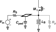
Does LB affect the performance of the circuit at resonance? Accompanying LB is the parallel equivalent resistance Rp = QLBω, which contributes noise and possibly attenuates the input signal. Thus, Rp must be at least ten times higher than RS = 50Ω. In other words, if the total capacitance at the input is so large as to dictate an excessively small inductor and Rp, then the noise figure is quite high. This situation may arise only at frequencies approaching the fT of the technology.
In the third step, the bias of M1 is defined by means of MB and IREF in Fig. 5.24. For example, WB = 0.2W1 and IREF = 0.2ID1 so that the bias branch draws only one-fifth of the current of the main branch.7 Capacitor CB provides a sufficiently low impedance (much less than 50Ω) from the gate of M1 to ground and also bypasses the noise of MB and IB to ground. The choice of a solid, low-inductance ground is critical here because the high-frequency performance of the CG stage degrades drastically if the impedance seen in series with the gate becomes comparable with RS.
Next, the width of M2 in Fig. 5.24 must be chosen (the length is the minimum allowable value). With the bias current known (ID2 = ID1), if the width is excessively small, then VGS2 may be so large as to drive M1 into the triode region. On the other hand, as W2 increases, M2 contributes an increasingly larger capacitance to node X while its gm reaches a nearly constant value (why?). Thus, the optimum width of M2 is likely to be near that of M1, and that is the initial choice. Simulations can be used to refine this choice, but in practice, even a twofold change from this value negligibly affects the performance.
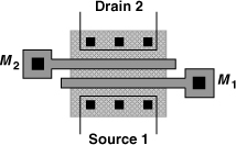
In order to minimize the capacitance at node X in Fig. 5.24, transistors M1 and M2 can be laid out such that the drain area of the former is shared with the source area of the latter. Furthermore, since no other connection is made to this node, the shared area need not accommodate contacts and can therefore be minimized. Depicted in Fig. 5.27 and feasible only if W1 = W2, such a structure can be expanded to one with multiple gate fingers.
Figure 5.27 Layout of cascode devices.
In the last step, the value of the load inductor, L1, must be determined (Fig. 5.24). In a manner similar to the choice of LB, we compute L1 such that it resonates with CGD2 + CDB2, the input capacitance of the next stage, and its own capacitance. Since the voltage gain of the LNA is proportional to R1 = QL1ω, R1 must be sufficiently large, e.g., 500 to 1000Ω. This condition is met in most designs without much difficulty.
The design procedure outlined above leads to a noise figure around 3 dB [Eq. (5.58)] and a voltage gain, Vout/Vin = R1/(2RS), of typically 15 to 20 dB. If the gain is too high, i.e., if it dictates an unreasonably high mixer IP3, then an explicit resistor can be placed in parallel with R1 to obtain the required gain. As studied in Section 5.7, this LNA topology displays a high IIP3, e.g., +5to +10 dBm.
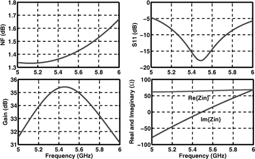
Solution:
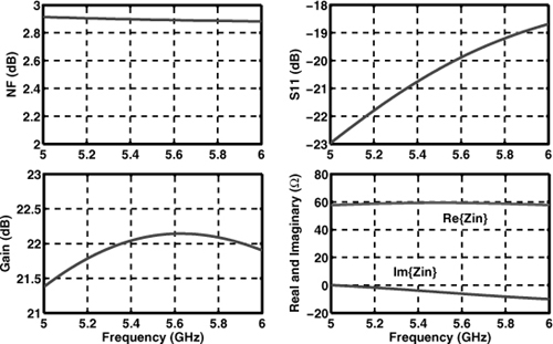
Figure 5.28 Transcoductance of a 10 μm/60 nm NMOS device as a function of drain current.
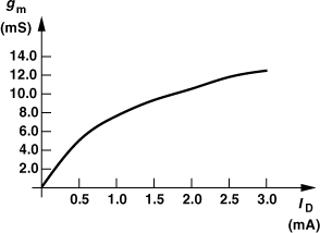

Figure 5.30 Simulated charactersitics of CG LNA example.
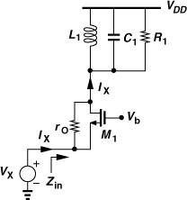
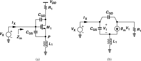
5.3.4 Cascode CS Stage with Inductive Degeneration
Our study of the CS stage of Fig. 5.11(a) indicates that the feedback through the gate-drain capacitance many be exploited to produce the required real part, but it also leads to a negative resistance at lower frequencies. We must therefore seek a topology in which the input is “isolated” from the inductive load and the input resistance is established by means other than CGD.
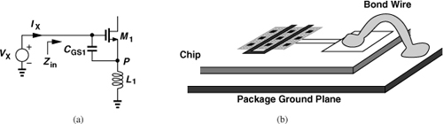
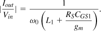
Let us first develop the latter concept. As mentioned in Section 5.2, we must employ active devices to provide a 50-Ω input resistance without the noise of a 50-Ω resistor. One such method employs a CS stage with inductive degeneration, as shown in Fig. 5.31(a). We first compute the input impedance of the circuit while neglecting CGD and CSB.9 Flowing entirely through CGS1, IX generates a gate-source voltage of IX/(CGS1s) and hence a drain current of gmIX/(CGS1s). These two currents flow through L1, producing a voltage
![]()
Figure 5.31 (a) Input impedance of inductively-degenerated CS stage, (b) use of bond wire for degeneration.
Since VX = VGS1 + VP, we have
![]()
Interestingly, the input impedance contains a frequency-independent real part given by gmL1/CGS1. Thus, the third term can be chosen equal to 50Ω.
The third term in Eq. (5.77) carries a profound meaning: since gm/CGS1 ≈ ωT(= 2πfT), the input resistance is approximately equal to L1ωT and directly related to the fT of the transistor. For example, in 65-nm technology, ωT ≈ 2π × (160 GHz), dictating L1 ≈ 50 pH (!) for a real part of 50Ω.
In practice, the degeneration inductor is often realized as a bond wire with the reasoning that the latter is inevitable in packaging and must be incorporated in the design. To minimize the inductance, a “downbond” can directly connect the source pad to a ground plane in the package [Fig. 5.31(b)], but even this geometry yields a value in the range of 0.5 to 1 nH—far from the 50-pH amount calculated above! That is, the input resistance provided by modern MOSFETs tends to be substantially higher than 50Ω if a bond wire inductance is used.10
How do we obtain a 50-Ω resistance with L1 ≈ 0.5 nH? At operation frequencies far below fT of the transistor, we can reduce the fT. This is accomplished by increasing the channel length or simply placing an explicit capacitor in parallel with CGS. For example, if L1 = 0.5 nH, then fT must be lowered to about 16 GHz.
Figure 5.32 (a) Input impedance of CS stage in the presence of CGD, (b) equivalent circuit.
Solution:
![]()
![]()
If R1 ≈ 1/gm ![]() |CGDs|−1 and CGS/CGD dominates in the denominator, (5.80) reduces to
|CGDs|−1 and CGS/CGD dominates in the denominator, (5.80) reduces to
![]()
Effect of Pad Capacitance
In addition to CGD, the input pad capacitance of the circuit also lowers the input resistance. To formulate this effect, we construct the equivalent circuit shown in Fig. 5.33(a), where CGS1, L1, and R1 represent the three terms in Eq. (5.77), respectively. Denoting the series combination jL1ω − j/(CGS1ω) by jX1 and −j/(Cpadω) by jX2, we first transform jX1 + R1 to a parallel combination [Fig. 5.33(b)]. From Chapter 2,
![]()
Figure 5.33 (a) Equivalent circuit for inclusion of pad capacitance, (b) simplified circuit of (a), (c) simplified circuit of (b).
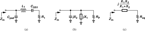
We now merge the two parallel reactances into jX1X2/(X1 + X2) and transform the resulting circuit to a series combination [Fig. 5.33(c)], where
In most cases, we can assume L1ω ![]() 1/(CGS1ω) + 1/(Cpadω) at the frequency of interest, obtaining
1/(CGS1ω) + 1/(Cpadω) at the frequency of interest, obtaining
![]()
For example, if CGS1 ≈ Cpad, then the input resistance falls by a factor of four.
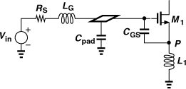
We can now make two observations. First, the effect of the gate-drain and pad capacitance suggests that the transistor fT need not be reduced so much as to create R1 = 50Ω. Second, since the degeneration inductance necessary for Re{Zin} = 50Ω is insufficient to resonate with CGS1 + Cpad, another inductor must be placed in series with the gate as shown in Fig. 5.34, where it is assumed LG is off-chip.
Figure 5.34 Addition of LG for input matching.
NF Calculation
Let us now compute the noise figure of the CS circuit, excluding the effect of channel-length modulation, body effect, CGD, and Cpad for simplicity (Fig. 5.35). The noise of M1 is represented by In1. For now, we assume the output of interest is the current Iout. We have
![]()
Figure 5.35 Equivalent circuit for computation of NF.
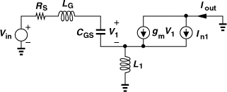
Also, since L1 sustains a voltage of L1s(Iout + V1CGS1s), a KVL around the input loop yields
![]()
Substituting for V1 from (5.86) gives
![]()
The input network is designed to resonate at the frequency of interest, ω0. That is, ![]() and hence, (L1 + LG)CGS1s2 + 1 = 0 at s = jω0. We therefore obtain
and hence, (L1 + LG)CGS1s2 + 1 = 0 at s = jω0. We therefore obtain
![]()
The coefficient of Iout represents the transconductance gain of the circuit (including RS):
Now, recall from Eq. (5.77) that, for input matching, gmL1/CGS1 = RS. Since gm/CGS1 ≈ ωT,
![]()
Interestingly, the transconductance of the circuit remains independent of L1, LG, and gm so long as the input is matched.
Setting Vin to zero in Eq. (5.89), we compute the output noise due to M1:
![]()
which, for gmL1/CGS1 = RS, reduces to
![]()
and hence
![]()
Dividing the output noise current by the transconductance of the circuit and by 4kTRS and adding unity to the result, we arrive at the noise figure of the circuit [2]:
![]()
It is important to bear in mind that this result holds only at the input resonance frequency and if the input is matched.
The above example suggests that maximizing LG can minimize the noise figure by providing voltage gain from Vin to the gate of M1. The reader can prove that this gain is given by
![]()
Note that LGω0/RS represents the Q of the series combination of LG and RS. Indeed, as explained below, the design procedure begins with the maximum available value of LG (typically an off-chip inductor) whose parasitic capacitances are negligible. The voltage gain in the input network (typically as high as 6 dB) does lower the IP3 and P1dB of the LNA, but the resulting values still prove adequate in most applications.
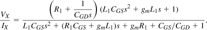
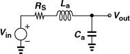
We now turn our attention to the output node of the circuit. As explained in Section 5.3.1, an inductive load attached to a common-source stage introduces a negative resistance due to the feedback through CGD. We therefore add a cascode transistor in the output branch to suppress this effect. Figure 5.37 shows the resulting circuit, where R1 models the loss of LD. The voltage gain is equal to the product of the circuit’s transconductance [Eq. (5.91)] and the load resistance, R1:12
Figure 5.37 Inductively-degenerated cascode CS LNA.
The effect of CGD1 on the input impedance may still require attention because the impedance seen at the source of M2, RX, rises sharply at the output resonance frequency. From Eq. (5.64),
![]()
Using the transconductance expression in (5.90) and VG/Vin in (5.96), we compute the voltage gain from the gate to the drain of M1:
![]()
Since RS ![]() L1ω0 (why?) and the second fraction is typically near or higher than unity, CGD1 may suffer from substantial Miller multiplication at the output resonance frequency.
L1ω0 (why?) and the second fraction is typically near or higher than unity, CGD1 may suffer from substantial Miller multiplication at the output resonance frequency.
In the foregoing noise figure calculation, we have not included the noise contribution of M2. As formulated for the cascode CG stage in Section 5.3.3, the noise of the cascode device begins to manifest itself if the frequency of operation exceeds roughly (2rO1CX)−1.
Design Procedure
Having developed a good understanding of the cascode CS LNA of Fig. 5.37, we now describe a procedure for designing the circuit. The reader is encouraged to review the CG design procedure. The procedure begins with four knowns: the frequency of operation, ω0, the value of the degeneration inductance, L1, the input pad capacitance, Cpad, and the value of the input series inductance, LG. Each of the last three knowns is somewhat flexible, but it is helpful to select some values, complete the design, and iterate if necessary.
Governing the design are the following equations:
With ω0 known, CGS1 is calculated from (5.102), and ωT and gm (=ωTCGS1) from (5.103). We then return to the plots of gm and fT in Fig. 5.25 and determine whether a transistor width can yield the necessary gm and fT simultaneously. In deep-submicron technologies and for operation frequencies up to a few tens of gigahertz, the fT is likely to be “too high,” but the pad capacitance alleviates the issue by transforming the input resistance to a lower value. If the requisite fT is quite low, a capacitance can be added to Cpad. On the other hand, if the pad capacitance is so large as to demand a very high fT, the degeneration inductance can be increased.
In the next step, the dimensions of the cascode device are chosen equal to those of the input transistor. As mentioned in Section 5.3.3 for the cascode CG stage, the width of the cascode device only weakly affects the performance. Also, the layout of M1 and M2 can follow the structure shown in Fig. 5.27 to minimize the capacitance at node X.
The design procedure now continues with selecting a value for LD such that it resonates at ω0 with the drain-bulk and drain-gate capacitances of M2, the input capacitance of the next stage, and the inductors’s own parasitic capacitance. If the parallel equivalent resistance of LD results in a gain, R1/(2L1ω0), greater than required, then an explicit resistor can be placed in parallel with LD to lower the gain and widen the bandwidth.
In the last step of the design, we must examine the input match. Due to the Miller multiplication of CGD1 (Example 5.12), it is possible that the real and imaginary parts depart from their ideal values, necessitating some adjustment in LG.
The foregoing procedure typically leads to a design with a relatively low noise figure, around 1.5 to 2 dB—depending on how large LG can be without displaying excessive parasitic capacitances. Alternatively, the design procedure can begin with known values for NF and L1 and the following two equations:

where the noise of the cascode transistor and the load is neglected. The necessary values of ωT and gm1 can thus be computed (gm1/CGS1 ≈ ωT). If the plots in Fig. 5.25 indicate that the device fT is too high, then additional capacitance can be placed in parallel with CGS1. Finally, LG is obtained from Eq. (5.102). (If advanced packaging minimizes inductances, then L1 can be integrated on the chip and assume a small value.)
The overall LNA appears as shown in Fig. 5.38, where the antenna is capacitively tied to the receiver to isolate the LNA bias from external connections. The bias current of M1 is established by MB and IB, and resistor RB and capacitor CB isolate the signal path from the noise of IB and MB. The source-bulk capacitance of M1 and the capacitance of the pad at the source of M1 may slightly alter the input impedance and must be included in simulations.
Figure 5.38 Inductively-degenerated CS stage with pads and bias network.
Solution:
Figure 5.39 (a) Effect of bias resistor RB on CS LNA, (b) conversion of RS and LG to a parallel network, (c) effect of distributed capacitance of RB.

The choice between the CG and CS LNA topologies is determined by the trade-off between the robustness of the input match and the lower bound on the noise figure. The former provides an accurate input resistance that is relatively independent of package parasitics, whereas the latter exhibits a lower noise figure. We therefore select the CG stage if the required LNA noise figure can be around 4 dB, and the CS stage for lower values.
An interesting point of contrast between the CG and CS LNAs relates to the contribution of the load resistor, R1, to the noise figure. Equation (5.58) indicates that in a CG stage, this contribution, 4RS/R1, is equal to 4 divided by the voltage gain from the input source to the output. Thus, for a typical gain of 10, this contribution reaches 0.4, a significant amount. For the inductively-degenerated CS stage, on the other hand, Eq. (5.101) reveals that the contribution is equal to 4RS/R1 multiplied by (ω0/ωT)2. Thus, for operation frequencies well below the fT of the transistor, the noise contribution of R1 becomes negligible.
Solution:
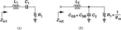
Figure 5.40 Input networks of (a) CS and (b) CG LNAs.
![]()
![]()
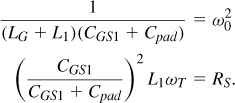
If the center frequency of interest is ![]() and ω = ω0 + Δω, then
and ω = ω0 + Δω, then
![]()
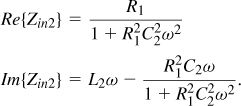
In practice, 1/(R1C2) is comparable with the ωT of the transistor [e.g., if R1 = 1/gm and C2 = CGS, then 1/(R1C2) ≈ ωT]. Thus, for ω ![]() ωT,
ωT,
![]()
![]()
Interestingly, if ![]() , then Im{Zin2} falls to zero and becomes independent of frequency. Thus the CG stage indeed provides a much broader band at its input, another advantage of this topology.
, then Im{Zin2} falls to zero and becomes independent of frequency. Thus the CG stage indeed provides a much broader band at its input, another advantage of this topology.
5.3.5 Variants of Common-Gate LNA
As revealed by Eq. (5.57), the noise figure and input matching of the CG stage are inextricably related if channel-length modulation is negligible, a common situation in older CMOS technologies. For this reason, a number of efforts have been made to add another degree of freedom to the design so as to avoid this relationship. In this section, we describe two such examples.
Figure 5.43 shows a topology incorporating voltage-voltage feedback [3].13 The block having a gain (or attenuation factor) of α senses the output voltage and subtracts a fraction thereof from the input. (Note that M1 operates as a subtractor because ID1 ∝ VF − Vin.) The loop transmission can be obtained by breaking the loop at the gate of M1 and is equal to gmZL · α.14 If channel-length modulation and body effect are neglected, the closed-loop input impedance is equal to the open-loop input impedance, 1/gm, multiplied by 1+gmZLα:
![]()
Figure 5.43 CG LNA with feedback.
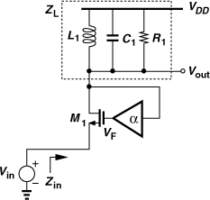
At resonance,
![]()
The input resistance can therefore be substantially higher than 1/gm, but how about the noise figure? We first calculate the gain with the aid of the circuit depicted in Fig. 5.44(a). The voltage gain from X to the output is equal to the open-loop gain, gmR1, divided by 1 + αgmR1 (at the resonance frequency). Thus,

Figure 5.44 (a) Input impedance and (b) noise behavior of CG stage with feedback.

which reduces to R1/(2RS) if the input is matched.
For output noise calculation, we construct the circuit of Fig. 5.44(b), where Vn1 represents the noise voltage of M1 and noise of the feedback circuit is neglected. Since RS carries a current equal to −Vn,out/R1 (why?), we recognize that VGS1 = αVn,out + Vn1 + Vn,outRS/R1. Equating gmVGS1 to −Vn,out/R1 yields
![]()
The noise current of R1 is multiplied by the output impedance of the circuit, Rout. The reader can show that Rout is equal to R1 in parallel with (1 + gmRS)/(αgm). Summing this noise and that of M1, dividing the result by the square of (5.116) and 4kTRS, and assuming the input is matched, we have
![]()
That is, the NF can be lowered by raising gm. Note that this result is identical to that expressed by Eq. (5.57) for the simple CG stage, except that gmRS need not be equal to unity here. For example, if gmRS = 4 and γ = 1, then the first two terms yield a noise figure of 0.97 dB. In Problem 5.15 we reexamine these results if channel-length modulation is not neglected.
Another variant of the CG LNA employs feedforward to avoid the tight relationship between the input resistance and the noise figure [4]. Illustrated in Fig. 5.45(a), the idea is to amplify the input by a factor of −A and apply the result to the gate of M1. For an input voltage change of ΔV, the gate-source voltage changes by −(1 + A)ΔV and the drain current by −(1 + A)gmΔV. Thus, the gm is “boosted” by a factor of 1 + A [4], lowering the input impedance to Rin = [gm(1 + A)]−1 and raising the voltage gain from the source to the drain to (1 + A)gmR1 (at resonance).
Figure 5.45 (a) CG stage with feedforward, (b) calculation of NF.
We now compute the noise figure with the aid of the equivalent circuit shown in Fig. 5.45(b). Since the current flowing through RS is equal to −Vn,out/R1, the source voltage is given by −Vn,outRS/R1 and the gate voltage by (−Vn,outRS/R1)(−A) + Vn1. Multiplying the gate-source voltage by gm and equating the result to −Vn,out/R1, we have
![]()
and hence
![]()
This expression reduces to −gmR1Vn1/2 if the input is matched, indicating that half of the noise current of M1 flows through R1.15 With input matching, the voltage gain from the left terminal of RS in Fig. 5.45(b) to the output is equal to (1 + A)gmR1/2. We therefore sum the output noise contribution of M1 and R1, divide the result by the square of this gain and the noise of RS, and add unity:
![]()
This equation reveals that the NF can be lowered by raising A with the constraint ![]() (for input matching).
(for input matching).
The above analysis has neglected the noise of the gain stage A in Fig. 5.45(a). We show in Problem 5.17 that the input-referred noise of this stage, ![]() , is multiplied by A and added to Vn1 in Eq. (5.122), leading to an overall noise figure equal to
, is multiplied by A and added to Vn1 in Eq. (5.122), leading to an overall noise figure equal to
In other words, ![]() is referred to the input by a factor of A2/(1 + A)2, which is not much less than unity. For this reason, it is difficult to realize A by an active circuit.
is referred to the input by a factor of A2/(1 + A)2, which is not much less than unity. For this reason, it is difficult to realize A by an active circuit.
It is possible to obtain the voltage gain through the use of an on-chip transformer. As shown in Fig. 5.46 [4], for a coupling factor of k between the primary and the secondary and a turns ratio of ![]() , the transformer provides a voltage gain of kn. The direction of the currents is chosen so as to yield a negative sign. However, on-chip transformer geometries make it difficult to achieve a voltage gain higher than roughly 3, even with stacked spirals [5]. Also, the loss in the primary and secondary contributes noise.
, the transformer provides a voltage gain of kn. The direction of the currents is chosen so as to yield a negative sign. However, on-chip transformer geometries make it difficult to achieve a voltage gain higher than roughly 3, even with stacked spirals [5]. Also, the loss in the primary and secondary contributes noise.
Figure 5.46 CG stage with transformer feedforward.
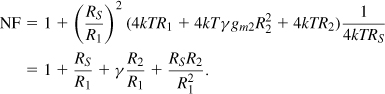
5.3.6 Noise-Cancelling LNAs
In our previous derivations of the noise figure of LNAs, we have observed three terms: a value of unity arising from the noise of RS itself, a term representing the contribution of the input transistor, and another related to the noise of the load resistor. “Noise-cancelling LNAs” aim to cancel the second term [6]. The underlying principle is to identify two nodes in the circuit at which the signal appears with opposite polarities but the noise of the input transistor appears with the same polarity. As shown in Fig. 5.47, if nodes X and Y satisfy this condition, then their voltages can be properly scaled and summed such that the signal components add and the noise components cancel.
Figure 5.47 Conceptual illustration of noise-cancelling LNAs.
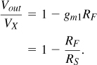
The CS stage with resistive feedback studied in Section 5.3.2 serves as a good candidate for noise cancellation because, as shown in Fig. 5.48(a), the noise current of M1 flows through RF and RS, producing voltages at the gate and drain of the transistor with the same polarity. The signal, on the other hand, experiences inversion. Thus, as conceptually shown in Fig. 5.48(b), if VX is amplified by −A1 and added to VY, the noise of M1 can be removed [6]. Since the noise voltages at nodes Y and X bear a ratio of 1 + RF/RS (why?), we choose A1 = 1+RF/RS. The signal experiences two additive gains: the original gain, VY/VX = 1 − gmRF = 1 − RF/RS (if the input is matched), and the additional gain, −(1 + RF/RS). It follows that
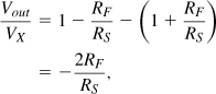
if the input is matched. The gain Vout/Vin is half of this value.
Figure 5.48 (a) Noise of input transistor in a feedback CS stage, (b) cancellation of noise of M1.

Let us now compute the noise figure of the circuit, assuming that the auxiliary amplifier exhibits an input-referred noise voltage VnA1 and a high input impedance. Recall from Section 5.3.2 that the noise voltage of RF appears directly at the output as 4kTRF. Adding this noise to ![]() , dividing the result by (RF/RS)2 and 4kTRS, and adding unity, we obtain the noise figure as
, dividing the result by (RF/RS)2 and 4kTRS, and adding unity, we obtain the noise figure as
![]()
Since A1 = 1 + RF/RS,

The NF can therefore be minimized by maximizing RF and minimizing ![]() . Note that RS/RF is the inverse of the gain and hence substantially less than unity, making the third term approximately equal to
. Note that RS/RF is the inverse of the gain and hence substantially less than unity, making the third term approximately equal to ![]() . That is, the noise of the auxiliary amplifier is directly referred to the input and must therefore be much less than that of RS.
. That is, the noise of the auxiliary amplifier is directly referred to the input and must therefore be much less than that of RS.
The input capacitance, Cin, arising from M1 and the auxiliary amplifier degrades both S11 and the noise cancellation, thereby requiring a series (or parallel) inductor at the input for operation at very high frequencies. It can be proved [6] that the frequency-dependent noise figure is expressed as
![]()
where NF(0) is given by (5.128) and f0 = 1/(πRSCin).
Figure 5.49 depicts an implementation of the circuit [6]. Here, M2 and M3 serve as a CS amplifier, providing a voltage gain of gm2/(gm3 + gmb3), and also as the summing circuit. Transistor M3 operates as a source follower, sensing the signal and noise at the drain of M1. The first stage is similar to that studied in Example 5.7.
Figure 5.49 Example of noise-cancelling LNA.
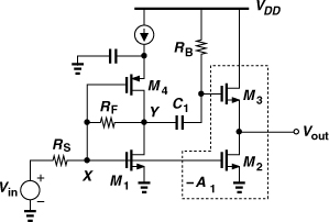
Figure 5.50 CG/CS stage as a noise-cancelling LNA.
Solution:
![]()
![]()
If the noise of M1 is cancelled, the noise figure arises from the contributions of M2, R1, and R2. The noise at Y is equal to 4kTR1 and at N equal to ![]() . Since the total voltage gain, Vout/Vin, is given by (gm1R1 + gm2R2)/2 = gm1R1 = R1/RS, we have
. Since the total voltage gain, Vout/Vin, is given by (gm1R1 + gm2R2)/2 = gm1R1 = R1/RS, we have
The principal advantage of the above noise cancellation technique is that it affords the broadband characteristics of feedback or CG stages but with a lower noise figure. It is therefore suited to systems operating in different frequency bands or across a wide frequency range, e.g., 900 MHz to 5 GHz.
5.3.7 Reactance-Cancelling LNAs
It is possible to devise an LNA topology that inherently cancels the effect of its own input capacitance. Illustrated in Fig. 5.51(a) [7], the idea is to exploit the inductive input impedance of a negative-feedback amplifier so as to cancel the input capacitance, Cin. If the open-loop transfer function of the core amplifier is modeled by a one-pole response, A0/(1 + s/ω0), then the input admittance is given by
![]()
Figure 5.51 (a) Reactance-cancelling LNA topology, (b) behavior of components of Y1 with frequency.


![]()
At frequencies well below ω0, 1/Re{Y1} reduces to RF/(1 + A0), which can be set equal to RS, and Im{Y1} is roughly −A0ω/(RFω0), which can be chosen to cancel Cinω. Figure 5.51(b) illustrates the behavior of 1/Re{Y1} and −Im{Y1}.
The input matching afforded by the above technique holds for frequencies up to about ω0, dictating that the open-loop bandwidth of the core amplifier reach the maximum frequency of interest. The intrinsic speed of deep-submicron devices provides the gain and bandwidth required here.
The reader may wonder if our modeling of the core amplifier by a one-pole response applies to multistage implementations as well. We return to this point below.
Figure 5.52 shows a circuit realization of the amplifier concept for the frequency range of 50 MHz to 10 GHz [7]. Three common-source stages provide gain and allow negative feedback. Cascodes and source followers are avoided to save voltage headroom. The input transistor, M1, has a large width commensurate with flicker noise requirements at 50 MHz, thus operating with a VGS of about 200 mV. If this voltage also appears at node Y, it leaves no headroom for output swings, limiting the linearity of the circuit. To resolve this issue, current I1 is drawn from RF so as to shift up the quiescent voltage at Y by approximately 250 mV. Since RF = 1 kΩ, I1 need be only 200 μA, contributing negligible noise at the LNA input.16
Figure 5.52 Implementation of reactance-cancelling LNA.
With three gain stages, the LNA can potentially suffer from a small phase margin and exhibit substantial peaking in its frequency response. In this design, the open-loop poles at nodes A, B, X, and Y lie at 10 GHz, 24.5 GHz, 22 GHz, and 75 GHz, respectively, creating a great deal of phase shift. Nonetheless, due to the small feedback factor, RS/(RS + RF) = 0.048, simulations indicate that the circuit provides a phase margin of about 50° and a peaking of 1 dB in its closed-loop frequency response.
The multi-pole LNA of Fig. 5.52 contains an inductive component in its input impedance but with a behavior more complex than the above analysis suggests. Fortunately, behavioral simulations confirm that, if the poles at B, X, and Y are “lumped” (i.e., their time constants are added), then the one-pole approximation still predicts the input admittance accurately. The pole frequencies mentioned above collapse to an equivalent value of ω0 = 2π (9.9 GHz), suggesting that the real and imaginary parts of Y1 retain the desired behavior up to the edge of the cognitive radio band.
The LNA output is sensed between nodes X and Y. Even though these nodes provide somewhat unequal swings and a phase difference slightly greater than 180°, the pseudo-differential sensing still raises both the gain and the IP2, the latter because second-order distortion at X also appears at Y and is thus partially cancelled in VY − VX.17
5.4 Gain Switching
The dynamic range of the signal sensed by a receiver may approach 100 dB. For example, a cell phone may receive a signal level as high as −10 dBm if it is close to a base station or as low as −110 dBm if it is in an underground garage. While designed for the highest sensitivity, the receiver chain must still detect the signal correctly as the input level continues to increase. This requires that the gain of each stage be reduced so that the subsequent stages remain sufficiently linear with the large input signal. Of course, as the gain of the receiver is reduced, its noise figure rises. The gain must therefore be lowered such that the degradation in the sensitivity is less than the increase in the received signal level, i.e., the SNR does not fall. Figure 5.53 shows a typical scenario.
Figure 5.53 Effect of gain switching on NF and P1dB.

Gain switching in an LNA must deal with several issues: (1) it must negligibly affect the input matching; (2) it must provide sufficiently small “gain steps”; (3) the additional devices performing the gain switching must not degrade the speed of the original LNA; (4) for high input signal levels, gain switching must also make the LNA more linear so that this stage does not limit the receiver linearity. As seen below, some LNA topologies lend themselves more easily to gain switching than others do.
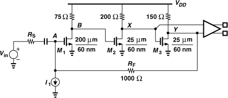
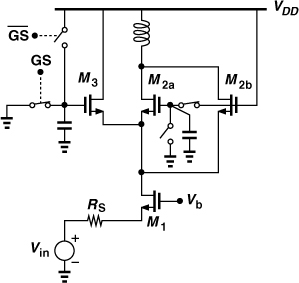
Let us first consider a common-gate stage. Can we reduce the transconductance of the input transistor to reduce the gain? To switch the gain while maintaining input matching, we can insert a physical resistance in parallel with the input as gm is lowered. Figure 5.54 shows an example [8], where the input transistor is decomposed into two, M1x and M1y, and transistor M2 introduces a parallel resistance if it is on. In the “high-gain mode,” the gain select line, GS, is high, placing M1x and M1y in parallel, and M2 is off. In the “low-gain mode,” M1y turns off, reducing the gain, and M2 turns on, ensuring that Ron2||(gm1x + gmb1x)−1 = RS. For example, to reduce the gain by 6 dB, we choose equal dimensions for M1x and M1y and Ron2 = (gm1x + gmb1x)−1 = 2RS (why?). Also, the gate of M1y is secured to ground by a capacitor to avoid the on-resistance of the switch at high frequencies.
Figure 5.54 Example of gain switching in CG stage.
Solution:
To reduce the voltage gain by ![]() , we have
, we have
![]()
and hence ![]() . We also note that, with M1y off, the input resistance rises to
. We also note that, with M1y off, the input resistance rises to ![]() . Thus,
. Thus, ![]() and hence
and hence
![]()
In the above calculation, we have neglected the effect of channel-length modulation. If the upper bound expressed by Eq. (5.67) restricts the design, then the cascode CG stage of Fig. 5.24 can be used.
Another approach to switching the gain of a CG stage is illustrated in Fig. 5.55, where the on-resistance of M2 appears in parallel with R1. With input matching and in the absence of channel-length modulation, the gain is given by
![]()
Figure 5.55 Effect of load switching on input impedance.
For multiple gain steps, a number of PMOS switches can be placed in parallel with R1. The following example elaborates on this point.
Solution:
![]()
Figure 5.56 Load switching for 3-dB gain steps.
i.e., ![]() . For the second 3-dB reduction, both M2a and M2b are turned on and
. For the second 3-dB reduction, both M2a and M2b are turned on and
![]()
i.e., ![]() . Note that if only M2b were on in this case, then it would need to be wider, thus contributing a greater capacitance to the output node.
. Note that if only M2b were on in this case, then it would need to be wider, thus contributing a greater capacitance to the output node.
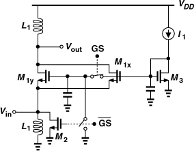
The principal difficulty with switching the load resistance in a CG stage is that it alters the input resistance, as expressed by Rin = (R1 + rO)/(1 + gmrO). This effect can be minimized by adding a cascode transistor as in Fig. 5.24. The use of a cascode transistor also permits a third method of gain switching. Illustrated in Fig. 5.57, the idea is to route part of the drain current of the input device to VDD—rather than to the load—by means of another cascode transistor, M3. For example, if M2 and M3 are identical, then turning M3 on yields α = 0.5, dropping the voltage gain by 6 dB.
Figure 5.57 Gain switching by cascode device.

The advantage of the above technique over the previous two is that the gain step depends only on W3/W2 (if M2 and M3 have equal lengths) and not the absolute value of the on-resistance of a MOS switch. The bias and signal currents produced by M1 split between M3 and M2 in proportion to W3/W2, yielding a gain change by a factor of 1 + W3/W2. As a result, gain steps in the circuit of Fig. 5.57 are more accurate than those in Figs. 5.54 and 5.55. However, the capacitance introduced by M3 at node Y degrades the performance at high frequencies. For a single gain step of 6 dB, we have W3 = W2, nearly doubling the capacitance at this node. For a gain reduction by a factor of N, W3 = (N − 1)W2, possibly degrading the performance considerably.
Solution:
In the high-gain mode, the input impedance is given by Eq. (5.70). In the low-gain mode, the impedance seen looking into the source of M2 changes because both gm2 and rO2 change. For a square-law device, a twofold reduction in the bias current (while the dimensions remain unchanged) translates to a twofold increase in rO and a ![]() reduction in gm. Thus, in Fig. 5.57,
reduction in gm. Thus, in Fig. 5.57,
![]()
![]()
![]()
In order to reduce the capacitance contributed by the gain switching transistor, we can turn off part of the main cascode transistor so as to create a greater imbalance between the two. Shown in Fig. 5.58 (on page 310) is an example where M2 is decomposed into two devices so that, when M3 is turned on, M2a is turned off. Consequently, the gain drops by a factor of 1 + W3/W2b rather than 1 + W3/(W2b + W2a).
Figure 5.58 Gain switching by programmable cascode devices.
We now turn our attention to gain switching in an inductively-degenerated cascode LNA. Can we switch part of the input transistor to switch the gain (Fig. 5.59)? Turning M1b off does not alter ωT because the current density remains constant. Thus, Re{Zin} = L1ωT is relatively constant, but Im{Zin} changes, degrading the input match. If the input match is somehow restored, then the voltage gain, R1/(2L1ω), does not change! Furthermore, the thermal noise of S1 degrades the noise figure in the high gain mode. For these reasons, gain switching must be realized in other parts of the circuit.
Figure 5.59 Gain switching in CS stage.
As with the CG LNA of Fig. 5.55, the gain can be reduced by placing one or more PMOS switches in parallel with the load [Fig. 5.60(a)]. Alternatively, the cascode switching scheme of Fig. 5.57 can be applied here as well [Fig. 5.60(b)]. The latter follows the calculations outlined in Example 5.24, providing well-defined gain steps with a moderate additional capacitance at node Y. It is important to bear in mind that cascode switching is attractive because it reduces the current flowing through the load by a well-defined ratio and it negligibly alters the input impedance of the LNA.
Figure 5.60 Gain switching in cascode CS stage by (a) load switching, (b) additional cascode device.
For the two variants of the CG stage studied in Section 5.3.3, gain switching can be realized by cascode devices as illustrated in Fig. 5.57. The use of feedback or feedforward in these topologies makes it difficult to change the gain through the input transistor without affecting the input match.
Lastly, let us consider gain switching in the noise-cancelling LNA of Fig. 5.48(b). Since VY/VX = 1 − RF/RS and Rin is approximately equal to 1/gm1 and independent of RF, the gain can be reduced simply by lowering the value of RF. Though not essential in the low-gain mode, noise cancellation can be preserved by adjusting A1 so that it remains equal to 1 + RF/RS.
Which one of the foregoing gain reduction techniques also makes the LNA more linear? None, except for the last one! Since the CG and CS stages retain the gate-source voltage swing (equal to half of the input voltage swing), their linearity improves negligibly. In the feedback LNA of Fig. 5.48(b), on the other hand, a lower RF strengthens the negative feedback, raising the linearity to some extent.
Receiver designs in which the LNA nonlinearity becomes problematic at high input levels can “bypass” the LNA in very-low-gain modes. Illustrated conceptually in Fig. 5.61, the idea is to omit the LNA from the signal path so that the mixer (presumably more linear) directly senses the received signal. The implementation is not straightforward if input matching must be maintained. Figure 5.62 depicts a common-gate example, where M1 is turned off, M2 is turned on to produce a 50-Ω resistance, and M3 is turned on to route the signal to the mixer.

Figure 5.62 Realization of LNA bypass.
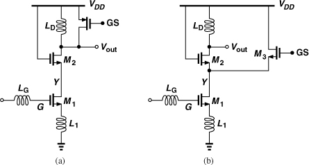
5.5 Band Switching
As mentioned in Section 5.1, LNAs that must operate across a wide bandwidth or in different bands can incorporate band switching. Figure 5.63(a) repeats the structure of Fig. 5.7(a), with the switch realized by a MOS transistor. Since the bias voltage at the output node is near VDD, the switch must be a PMOS device, thus contributing a larger capacitance for a given on-resistance than an NMOS transistor. This capacitance lowers the tank resonance frequency when S1 is off, reducing the maximum tolerable value of C1 and hence limiting the size of the input transistor of the following stage. (If L1 is reduced to compensate for the higher capacitance, then so are R1 and the gain.) For this reason, we prefer the implementation in Fig. 5.63(b), where S1 is formed as an NMOS device tied to ground.
Figure 5.63 (a) Band switching, (b) effect of switch parasitics.

The choice of the width of S1 in Fig. 5.63(b) proves critical. For a very narrow transistor, the on-resistance, Ron1, remains so high that the tank does not “feel” the presence of C2 when S1 is on. For a moderate device width, Ron1 limits the Q of C2, thereby lowering the Q of the overall tank and hence the voltage gain of the LNA. This can be readily seen by transforming the series combination of C2 and Ron1 to a parallel network consisting of C2 and RP1 ≈ Q2Ron1, where Q = (C2ωRon1)−1. That is, R1 is now shunted by a resistance ![]() .
.
The foregoing observation implies that Ron1 must be minimized such that RP1 ![]() R1. However, as the width of S1 in Fig. 5.63(b) increases, so does the capacitance that it introduces in the off state. The equivalent capacitance seen by the tank when S1 is off is equal to the series combination of C2 and CGD1 + CDB1, which means C1 must be less than its original value by this amount. We therefore conclude that the width of S1 poses a trade-off between the tolerable value of C1 when S1 is off and the reduction of the gain when S1 is on. (Recall that C1 arises from Ma, the input capacitance of the next stage, and the parasitic capacitance of L1.)
R1. However, as the width of S1 in Fig. 5.63(b) increases, so does the capacitance that it introduces in the off state. The equivalent capacitance seen by the tank when S1 is off is equal to the series combination of C2 and CGD1 + CDB1, which means C1 must be less than its original value by this amount. We therefore conclude that the width of S1 poses a trade-off between the tolerable value of C1 when S1 is off and the reduction of the gain when S1 is on. (Recall that C1 arises from Ma, the input capacitance of the next stage, and the parasitic capacitance of L1.)
An alternative method of band switching incorporates two or more tanks as shown in Fig. 5.64 [8]. To select one band, the corresponding cascode transistor is turned on while the other remains off. This scheme requires that each tank drive a copy of the following stage, e.g., a mixer. Thus, when M1 and band 1 are activated, so is mixer MX1. The principal drawback of this approach is the capacitance contributed by the additional cascode device(s) to node Y. Also, the spiral inductors have large footprints, making the layout and routing more difficult.
Figure 5.64 Band switching by programmable cascode branches.

5.6 High-IP2 LNAs
As explained in Chapter 4, even-order distortion can significantly degrade the performance of direct-conversion receivers. Since the circuits following the downconversion mixers are typically realized in differential form,18 they exhibit a high IP2, leaving the LNA and the mixers as the IP2 bottleneck of the receivers. In this section, we study techniques of raising the IP2 of LNAs, and in Chapter 6, we do the same for mixers.
5.6.1 Differential LNAs
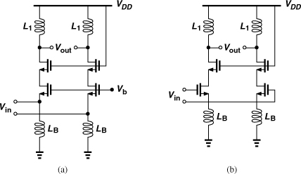
Differential LNAs can achieve high IP2’s because, as explained in Chapter 2, symmetric circuits produce no even-order distortion. Of course, some (random) asymmetry plagues actual circuits, resulting in a finite, but still high, IP2.
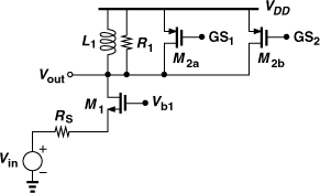
In principle, any of the single-ended LNAs studied thus far can be converted to differential form. Figure 5.65 depicts two examples. Not shown here, the bias network for the input transistors is similar to those described in Sections 5.3.3 and 5.3.4.
Figure 5.65 Differential (a) CG and (b) CS stages.
But what happens to the noise figure of the circuit if it is converted to differential form? Before answering this question, we must determine the source impedance driving the LNA. Since the antenna and the preselect filter are typically single-ended, a transformer must precede the LNA to perform single-ended to differential conversion. Illustrated in Fig. 5.66(a), such a cascade processes the signal differentially from the input port of the LNA to the end of the baseband section. The transformer is called a “balun,” an acronym for “balanced-to-unbalanced” conversion because it can also perform differential to single-ended conversion if its two ports are swapped.
Figure 5.66 (a) Use of balun at RX input, (b) simplified circuit.

If the source impedance provided by the antenna and the band-pass filter in Fig. 5.66(a) is RS1 (e.g., 50Ω), what is the differential source impedance seen by the LNA, RS2? For a lossless 1-to-1 balun, i.e., for a lossless transformer with an equal number of turns in its primary and secondary, we have RS2 = RS1. We must thus obtain the noise figure of the differential LNA with respect to a differential source impedance of RS1. Figure 5.66(b) shows the setup for output noise calculation.
Note that the differential input impedance of the LNA, Rin, must be equal to RS1 for proper input matching. Thus, in the LNAs of Figs. 5.66(a) and (b), the single-ended input impedance of each half circuit must be equal to RS1/2, e.g., 25Ω.
Differential CG LNA
We now calculate the noise figure of the differential CG LNA of Fig. 5.65(a), assuming it is designed such that the impedance seen between each input node and ground is equal to RS1/2. In other words, each CG transistor must provide an input resistance of 25Ω. Figure 5.67(a) shows the simplified environment, emphasizing that the noise figure is calculated with respect to a source impedance of RS1. Redrawing Fig. 5.67(a) as shown in Fig. 5.67(b), we recognize from the symmetry of the circuit that we can compute the output noise of each half circuit as in Fig. 5.67(c) and add the output powers:
![]()
Figure 5.67 (a) Cascade of balun and LNA, (b) simplified circuit of (a), and (c) simplified circuit of (b).
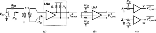
Since each half circuit provides matching at the input, the CG results of Section 5.3.3 apply here as well with the substitution RS = RS1/2. Specifically, the voltage gain from X to Y is equal to R1/(2RS1/2), where R1 denotes the load resistance of the CG half circuit. The output noise consists of (1) the input transistor contribution, given by Eq. (5.56), (2) the load resistor contribution, 4kTR1, and (3) the source impedance contribution, (4kTRS1/2)[R1/(2R1/2)]:
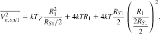
From Eq. (5.148), the total output noise power is twice this amount. Noting that the total voltage gain Av = (VY − VW)/(VX − VZ) is equal to that of half of the circuit, VY/VX( = R1/RS1), we compute the noise figure with respect to a source impedance of RS1 as
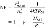
Interestingly, this value is lower than that of the single-ended counterpart [Eq. (5.58)]. But why? Since in Fig. 5.67(c), VY/VX = R1/(2RS1/2) = R1/RS1, we observe that the voltage gain is twice that of the single-ended CG LNA. (After all, the transconductance of the input transistor is doubled to lower the input impedance to RS1/2.) On the other hand, the overall differential circuit contains two R1’s at its output, each contributing a noise power of 4kTR1. The total, 8kTR1, divided by (R1/RS1)2 and 4kTRS1 yields 2RS1/R1. Of course, the value stipulated by Eq. (5.151) can be readily obtained in a single-ended CG LNA by simply doubling the load resistance. Figure 5.68 summarizes the behavior of the two circuits, highlighting the greater voltage gain in the differential topology. If identical gains are desired, the value of the load resistors in the differential circuit must be halved, thereby yielding identical noise figures.
Figure 5.68 Comparison of (a) single-ended and (b) differential CG LNAs.
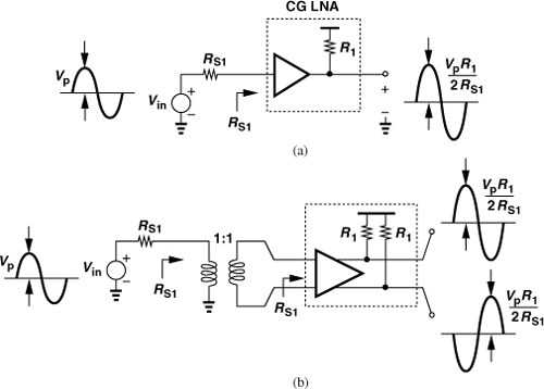
In summary, a single-ended CG LNA can be converted to differential form according to one of three scenarios: (1) simply copy the circuit, in which case the differential input resistance reaches 100Ω, failing to provide matching with a 1-to-1 balun; (2) copy the circuit but double the transconductance of the input transistors, in which case the input is matched but the overall voltage gain is doubled; (3) follow the second scenario but halve the load resistance to retain the same voltage gain. The second choice is generally preferable. Note that, for a given noise figure, a differential CG LNA consumes four times the power of a single-ended stage.19
Our NF calculations have assumed an ideal balun. In reality, even external baluns have a loss as high as 0.5 dB, raising the NF by the same amount.
Figure 5.69 (a) NF of an LNA with resistive termination, (b) differential version of (a), (c) simplified circuit of (b).

Solution:
In the circuit of Fig. 5.69(a), the amplifier input-referred noise current is negligible and the total noise at the output is equal to ![]() . The noise figure of the single-ended circuit is therefore given by
. The noise figure of the single-ended circuit is therefore given by

For the differential version, we write from the simplified half circuit shown in Fig. 5.69(c), ![]() . The total output noise power of the differential circuit is twice this amount. The corresponding noise figure is then given by
. The total output noise power of the differential circuit is twice this amount. The corresponding noise figure is then given by

Differential CS LNA
The differential CS LNA of Fig. 5.65(b) behaves differently from its CG counterpart. From Section 5.3.4, we recall that the input resistance of each half circuit is equal to L1ωT and must now be halved. This is accomplished by halving L1. With input matching and a degeneration inductance of L1, the voltage gain was found in Section 5.3.4 to be R1/(2L1ω0), which is now doubled. Figure 5.70(a) illustrates the overall cascade of the balun and the differential LNA. We assume that the width and bias current of each input transistor are the same as those of the single-ended LNA.
Figure 5.70 (a) Differential CS LNA and (b) its half circuit.
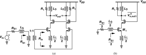
To compute the noise figure, let us first determine the output noise of the half circuit depicted in Fig. 5.70(b). Neglecting the contribution of the cascode device, we note from Section 5.3.4 that, if the input is matched, half of the noise current of the input transistor flows from the output node. Thus,
![]()
Multiplying this power by two, dividing it by ![]() and 4kTRS1, and noting that L1ωT/2 = RS1/2, we have
and 4kTRS1, and noting that L1ωT/2 = RS1/2, we have
![]()
How does this compare with the noise figure of the original single-ended LNA [Eq. (5.101)]? We observe that both the transistor contribution and the load contribution are halved. The transistor contribution is halved because gm1 and hence the transistor noise current remain unchanged while the overall transconductance of the circuit is doubled. To understand this point, recall from Section 5.3.4 that Gm = ωT/(2ω0RS) for the original single-ended circuit. Now consider the equivalent circuit shown in Fig. 5.71, where the differential transconductance, (I1 − I2)/Vin, is equal to ωT/(ω0RS1) (why?). The differential output current contains the noise currents of both M1 and M2 and is equal to 2(kTγgm1). If this power is divided by the square of the transconductance and 4kTRS1, the first term in Eq. (5.157) is obtained.
Figure 5.71 Differential CS stage viewed as a transconductor.
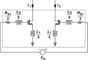
The reduction of the input transistor noise contribution in Eq. (5.157) is a remarkable property of differential operation, reinforcing the NF advantage of the degenerated CS stage over the CG LNA. However, this result holds only if the design can employ two degeneration inductors, each having half the value of that in the single-ended counterpart. This is difficult with bond wires as their physical length cannot be shortened arbitrarily. Alternatively, the design can incorporate on-chip degeneration inductors while converting the effect of the (inevitable) bond wire to a common-mode inductance. Figure 5.72 shows such a topology. With perfect symmetry, the bond wire inductance has no effect on the differential impedance seen between the gates. Nonetheless, as explained in Chapter 7, on-chip inductors suffer from a low quality factor (e.g., a high series resistance), possibly degrading the noise figure. We compare the power consumptions of the single-ended and differential implementations in Problem 5.22.
Figure 5.72 Differential CS stage with on-chip degeneration inductors.
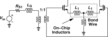
The NF advantage implied by Eq. (5.157) may not materialize in reality because the loss of the balun is not negligible.
Is it possible to use a differential pair to convert the single-ended antenna signal to differential form? As shown in Fig. 5.73(a), the signal is applied to one input while the other is tied to a bias voltage. At low to moderate frequencies, VX and VY are differential and the voltage gain is equal to gm1,2RD. At high frequencies, however, two effects degrade the balance of the phases: the parasitic capacitance at node P attenuates and delays the signal propagating from M1 to M2, and the gate-drain capacitance of M1 provides a non-inverting feedforward path around M1 (whereas M2 does not contain such a path).
Figure 5.73 Single-ended to differential conversion by (a) a simple differential pair, (b) a differential pair including tail resonance.
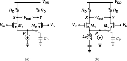
The capacitance at P can be nulled through the use of a parallel inductor [Fig. 5.73(b)] [9], but the CGD1 feedforward persists. The tail inductor can be realized on-chip because its parallel equivalent resistance at resonance (RP = QLPω0) is typically much greater than 1/gm1,2.
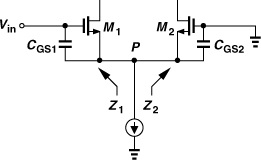
The topology of Fig. 5.73(b) still does not provide input matching. We must therefore insert (on-chip) inductances in series with the sources of M1 and M2 (Fig. 5.75). Here, LP1 and LP2 resonate with CP1 and CP2, respectively, and LS1 + LS2 provides the necessary input resistance. Of course, LS1 + LS2 is realized as one inductor. However, as explained in Section 5.7, this topology exhibits a lower IP3 than that of Fig. 5.65(b).
Figure 5.75 Use of on-chip inductors for resonance and degeneration.
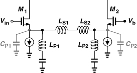
Balun Issues
The foregoing development of differential LNAs has assumed ideal 1-to-1 baluns. Indeed, external baluns with a low loss (e.g., 0.5 dB) in the gigahertz range are available from manufacturers, but they consume board space and raise the cost. Integrated baluns, on the other hand, suffer from a relatively high loss and large capacitances. Shown in Fig. 5.76 is an example, where two spiral inductors LAC and LCB are intertwined to create a high mutual coupling. As explained in Chapter 7, the resistance and capacitance associated with the spirals and the sub-unity coupling factor make such baluns less attractive.
Figure 5.76 Simple planar 1-to-1 balun.


The reader may wonder if an N-to-1 (rather than 1-to-N) balun proves beneficial in the above example as it would multiply the first two terms of Eq. (5.160) by 1/N2 rather than N2. Indeed, off-chip baluns may provide a lower noise figure if L1 (a bond wire) can be reduced by a factor of N2. On the other hand, on-chip baluns with a non-unity turns ratio are difficult to design and suffer from a higher loss and a lower coupling factor. Figure 5.78(a) shows an example [5], where one spiral forms the primary (secondary) of the balun and the series combination of two spirals constitutes the secondary (primary). Alternatively, as shown in Fig. 5.78(b), spirals having different numbers of turns can be embedded [10].
Figure 5.78 Realization of 1-to-2 balun as (a) stacked spirals, (b) embedded spirals.
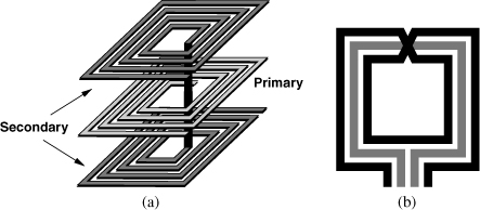
5.6.2 Other Methods of IP2 Improvement
The difficulty with the use of off-chip or on-chip baluns at the input of differential LNAs makes single-ended topologies still an attractive choice. A possible approach to raising the IP2 entails simply filtering the low-frequency second-order intermodulation product, called the beat component in Chapter 4. Illustrated in Fig. 5.79, the idea is to remove the beat by a simple high-pass filter (HPF) following the LNA. For example, suppose two interferers are located at the edges of the 2.4-GHz band, f1 = 2.4 GHz and f2 = 2.480 GHz. The beat therefore lies at 80 MHz and is attenuated by approximately a factor of 2400/80 = 30 for a first-order HPF. With this substantial suppression, the IP2 of the LNA is unlikely to limit the RX performance, calling for techniques that improve the IP2 of mixers (Chapter 6).
Figure 5.79 Removal of low-frequency beat by first-order high-pass filter.
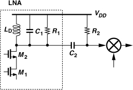
The filtration of the IM2 product becomes less effective for wider communication bands. For example, if a receiver must accommodate frequencies from 1 GHz to 10 GHz, then two interferers can produce a beat within the band, prohibiting the use of filters to remove the beat. In this case, the LNA may become the receiver’s IP2 bottleneck.
5.7 Nonlinearity Calculations
The general behavior of nonlinear systems was formulated in Chapter 2. In this section, we develop a methodology for computing the nonlinear characteristics of some circuits.
Recall from Chapter 2 that systems with weak static nonlinearity can be approximated by a polynomial such as y = α1x + α2x2 + α3x3. Let us devise a method for computing α1-α3 for a given circuit. In many circuits, it is difficult to derive y as an explicit function of x. However, we recognize that
![]()
![]()
![]()
These expressions prove useful because we can obtain the derivatives by implicit differentiation. It is important to note that in most cases, x = 0 in fact corresponds to the bias point of the circuit with no input perturbation. In other words, the total y may not be zero for x = 0. For example, in the common-source stage of Fig. 5.80, M1 is biased at a gate-source voltage of VGS0 = Vb and Vin is superimposed on this voltage.
Figure 5.80 CS stage with gate bias.

5.7.1 Degenerated CS Stage
As an example, let us study the resistively-degenerated common-source stage shown in Fig. 5.81, assuming the drain current is the output of interest. We wish to compute the IP3 of the circuit. For a simple square-law device
![]()
where K = (1/2)μnCox(W/L) and channel-length modulation and body effect are neglected. Since VGS = Vin − RSID,
![]()
and hence
![]()
Figure 5.81 CS stage for nonlinearity calculations.

We also note that
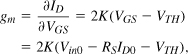
where Vin0 ( = Vb) and ID0 denote the bias values. Thus, in the absence of signals,
![]()
an expected result.
We now compute the second derivative from Eq. (5.166):
![]()
With no signals, (5.168) and (5.169) can be substituted in (5.170) to produce
![]()
Lastly, we determine the third derivative from (5.170):

which, from (5.169) and (5.171) reduces to
![]()
While lengthy, the foregoing calculations lead to interesting results. Equation (5.173) reveals that α3 = 0 if RS = 0, an expected outcome owing to the square-law behavior assumed for the transistor. Additionally, α1 and α3 have opposite signs, implying a compressive characteristic—whereas the undegenerated transistor would exhibit an expansive behavior. In other words, resistive degeneration of a square-law device creates third-order distortion.
To compute the IP3 of the stage, we write from Chapter 2,

The 1-dB compression point follows the same expression but lowered by a factor of 3.03 (9.6 dB).
The reader may wonder if the above analysis of nonlinearity confuses large-signal and small-signal operations by expression α1-α3 in terms of the device transconductance. It is helpful to bear in mind that gm in the above expressions is merely a short-hand notation for a constant value, 2K(Vin0 − RSID0 − VTH), and independent of the input. It is, of course, plausible that α1-α3 must be independent of the input; otherwise, the polynomial’s order exceeds 3.


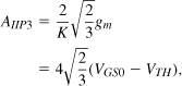
5.7.2 Undegenerated CS Stage
Consider the CS stage shown in Fig. 5.80. Submicron transistors substantially depart from square-law characteristics. The effect of mobility degradation due to both vertical and lateral fields in the channel can be approximated as
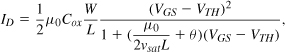
where μ0 denotes the zero-field mobility, vsat the saturation velocity of the carriers, and θ the effect of the vertical field [11]. If the second term in the denominator remains much less than unity, we can write (1 + ε)−1 ≈ 1 − ε and hence
![]()
The input signal, Vin, is superimposed on a bias voltage, VGS0 = Vb. We therefore replace VGS with Vin + VGS0, obtaining
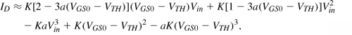
where K = (1/2)μ0Cox(W/L) and a = μ0/(2vsatL)+θ. We recognize the coefficient of Vin as the transconductance (∂ID/∂Vin) and the last two terms as the bias current. It follows that
![]()
![]()
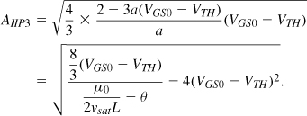
We note that the IP3 rises with the bias overdrive voltage, reaching a maximum of
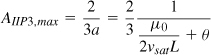
at VGS0 − VTH = (3a)−1 (Fig. 5.84).
Figure 5.84 Behavior of IP3 as a function of overdrive.

Solution:
The additional term a2(VGS − VTH)2 is multiplied by K(VGS − VTH)2, yielding two terms of interest: 4Ka2Vin(VGS − VTH)3 and ![]() . The former contributes to α1 and the latter to α3. It follows that
. The former contributes to α1 and the latter to α3. It follows that
![]()
![]()
5.7.3 Differential and Quasi-Differential Pairs
In RF systems, differential signals can be processed using the differential pair shown in Fig. 5.85(a) or the “quasi-differential” pair depicted in Fig. 5.85(b). The two topologies exhibit distinctly different nonlinear characteristics. We know from our above analysis that the dependence of the mobility upon vertical and lateral fields in the channel results in third-order nonlinearity in the quasi-differential pair and an IP3 given by Eq. (5.189). To study the nonlinearity of the standard differential pair, we recall from basic analog circuits that
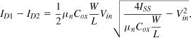
Figure 5.85 (a) Differential and (b) quasi-differential pairs.
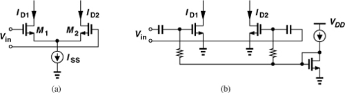
where Vin denotes the input differential voltage. If |Vin| ![]() ISS/(μnCoxW/L), then
ISS/(μnCoxW/L), then
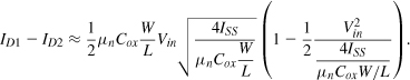
That is,
![]()
![]()
and hence
where (VGS0 − VTH) is the overdrive voltage of each transistor in equilibrium (Vin = 0).23
Interestingly, the standard differential pair suffers from third-order nonlinearity even in the absence of field-dependent mobility (i.e., with square-law devices). For this reason, the quasi-differential pair of Fig. 5.85(b) is preferred in cases where linearity is important. In fact, it is for this reason that the differential CS LNA of Fig. 5.65(b) does not employ a tail current source. The quasi-differential pair also saves the voltage headroom associated with the tail current source, proving more attractive as the supply voltage is scaled down.
5.7.4 Degenerated Differential Pair
Consider the degenerated pair shown in Fig. 5.86, where ID1 − ID2 is the output of interest. Since ID1 + ID2 = 2I0, we have ∂(ID1 − ID2)/∂Vin = 2∂ID1/∂Vin. Also, Vin1 − VGS1 − ISRS = Vin2 − VGS2 and IS = ID1 − I0. It follows that
![]()
Figure 5.86 Degenerated differential pair.
where Vin = Vin1 − Vin2 and K = (1/2)μnCox(W/L). Differentiating both sides with respect to Vin yields
![]()
At Vin = 0, ID1 = ID2 and

where gm = 2I0/(VGS0 − VTH). Differentiating both sides of (5.200) with respect to Vin gives
![]()
Note that for Vin = 0, we have ![]() because ∂ID1/∂Vin = −∂ID2/∂Vin and the term in the second set of square brackets vanishes. Differentiating once more and exploiting this fact, we have
because ∂ID1/∂Vin = −∂ID2/∂Vin and the term in the second set of square brackets vanishes. Differentiating once more and exploiting this fact, we have

It follows that ![]() . We now have that
. We now have that
![]()
References
[1] J. Rogin et al., “A 1.5-V 45-mW Direct-Conversion WCDMA Receiver IC in 0.13-m CMOS,” IEEE Journal of Solid-State Circuits, vol. 38, pp. 2239–2248, Dec. 2003.
[2] D. K. Shaeffer and T. H. Lee, “A 1.5-V, 1.5-GHz CMOS Low Noise Amplifier,” IEEE J. Solid-State Circuits, vol. 32, pp. 745–759, May 1997.
[3] P. Rossi et al., “A Variable-Gain RF Front End Based on a Voltage-Voltage Feedback LNA for Multistandard Applications,” IEEE J. Solid-State Circuits, vol. 40, pp. 690–697, March 2005.
[4] X. Li, S. Shekar, and D. J. Allstot, “Gm-Boosted Common-Gate LNA and Differential Colpitts VCO/QVCO in 0.18-um CMOS,” IEEE J. Solid-State Circuits, vol. 40, pp. 2609–2618, Dec. 2005.
[5] A. Zolfaghari, A. Y. Chan, and B. Razavi, “Stacked Inductors and 1-to-2 Transformers in CMOS Technology,” IEEE Journal of Solid-State Circuits, vol. 36, pp. 620–628, April 2001.
[6] F. Bruccoleri, E. A. M. Klumperink, and B. Nauta, “Wideband CMOS Low-Noise Amplifier Exploiting Thermal Noise Canceling,” IEEE J. Solid-State Circuits, vol. 39, pp. 275–281, Feb. 2004.
[7] B. Razavi, “Cognitive Radio Design Challenges and Techniques,” IEEE Journal of Solid-State Circuits, vol. 45, pp. 1542–1553, Aug. 2010.
[8] B. Razavi et al., “A UWB CMOS Transceiver,” IEEE Journal of Solid-State Circuits, vol. 40, pp. 2555–2562, Dec. 2005.
[9] M. Zargari et al., “A Single-Chip Dual-Band Tri-Mode CMOS Transceiver for IEEE 802.11a/b/g Wireless LAN,” IEEE Journal of Solid-State Circuits, vol. 39, pp. 2239–2249, Dec. 2004.
[10] J. R. Long and M. A. Copeland, “The Modeling, Characterization, and Design of Monolithic Inductors for Silicon RF ICs,” IEEE J. Solid-State Circuits, vol. 32, pp. 357–369, March 1997.
[11] B. Razavi, Design of Analog CMOS Integrated Circuits, Boston: McGraw-Hill, 2001.
Problems
5.1. Assuming Zin = x + jy, derive an equation for constant-τ contours in Fig. 5.4.
5.2. If Rp = RS and gmRS ≈ 1, determine the NF in Eq. (5.18) by considering the first three terms. What value of gm is necessary to achieve a noise figure of 3.5 dB?
5.3. Repeat Example 5.5 by solving the specific network shown in Fig. 5.10(a).
5.4. Determine the noise figure of the stages shown in Fig. 5.87 with respect to a source impedance of RS. Neglect channel-length modulation and body effect.
Figure 5.87 Stages for NF calculation.
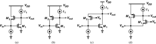
5.5. For the inductively-loaded CS stage of Fig. 5.11(b), determine Vout/Vin and find the voltage gain at the resonance frequency, ![]() , if |jC1ω0|
, if |jC1ω0| ![]() gm.
gm.
5.6. For the CS stage of Fig. 5.13(a), determine the closed-loop gain and noise figure if channel-length modulation is not neglected. Assume matching at the input.
5.7. For the complementary stage shown in Fig. 5.15, determine the closed-loop gain and noise figure if channel-length modulation is not neglected. Assume matching at the input.
5.8. For the CG stage of Fig. 5.16(a), compute the noise figure at the output resonance frequency if gm ≠ 1/RS. How can gm be chosen to yield a noise figure lower than 1 + γ + 4RS/Ra?
5.9. A circuit exhibits a noise figure of 3 dB. What percentage of the output noise power is due to the source resistance, RS? Repeat the problem for NF = 1 dB.
5.10. Determine the noise figure of the CG circuits shown in Fig. 5.17.
5.11. In Example 5.10, we concluded that the noise of M2 reaches the output unattenuated if ω is greater than (R1CX)−1 but much less than gm2/(CGS2 + CX). Does such a frequency range exist? In other words, under what conditions do we have (R1CX)−1 < ω ![]() gm2/(CGS2 + CX) >? Assume gm2 ≈ gm1 and recall that gm1R1 is the gain of the LNA and CX is on the order of CSG2.
gm2/(CGS2 + CX) >? Assume gm2 ≈ gm1 and recall that gm1R1 is the gain of the LNA and CX is on the order of CSG2.
5.12. If LG in Fig. 5.34 suffers from a series resistance of Rt, determine the noise figure of the circuit.
5.13. The LNA shown in Fig. 5.88 is designed to operate with low supply voltages. Each inductor is chosen to resonate with the total capacitance at its corresponding node at the frequency of interest. Neglect channel-length modulation and body effect and the noise due to the loss in L2. Determine the noise figure of the LNA with respect to a source resistance RS assuming that L1 can be viewed as a resistance equal to Rp at the resonance frequency. Make sure the result reduces to a familiar form if Rp → ∞. (Hint: the equivalent transconductance of a degenerated common-source stage is given by gm/(1 + gmR1), where R1 denotes the degeneration resistance.)
Figure 5.88 Folded-cascode LNA.

5.14. Determine S11 for both topologies in Fig. 5.40 and compute the maximum deviation of the center frequency for which S11 remains lower than −10 dB.
5.15. Repeat the analysis of the CG stage in Fig. 5.43 while including channel-length modulation.
5.16. Repeat the NF analysis of the CG stage in Fig. 5.43 while including the noise of the feedback network as a voltage, ![]() , in series with its input.
, in series with its input.
5.17. Prove that the input-referred noise of the feedforward amplifier in Fig. 5.45(a) manifests itself as the fourth term in Eq. (5.124).
5.18. Repeat the analysis of the CG stage of Fig. 5.45(a) while including channel-length modulation.
5.19. Is the noise of RF in Fig. 5.48(b) cancelled? Explain.
5.20. For the circuit shown in Fig. 5.89, we express the input-output characteristic as
![]()
where I0 and V0 denote the bias values, i.e., the values in the absence of signals. We note that ∂Iout/∂Vin = α1 at Vin = V0 (or Iout = I0). Similarly, ![]() at Vin = V0 (or Iout = I0).
at Vin = V0 (or Iout = I0).
Figure 5.89 Stage for IP2 calculation.
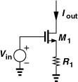
(a) Write a KVL around the input network in terms of Vin and Iout (with no VGS). Differentiate both sides implicitly with respect to Vin. You will need this equation in part (b). Noting that ![]() , where K = μnCoxW/L, find ∂Iout/∂Vin and hence α1.
, where K = μnCoxW/L, find ∂Iout/∂Vin and hence α1.
(b) Differentiate the equation obtained in part (a) with respect to Vin once more and compute α2 in terms of I0 and gm.
(c) Determine the IP2 of the circuit.
5.21. Determine the noise figure in Example 5.21 if the gain is reduced by 3 dB.
5.22. Compare the power consumptions of the single-ended and differential CS stages discussed in Section 5.6.1. Consider two cases: (a) the differential stage is derived by only halving L1 (and hence has a lower noise figure), or (b) the differential stage is designed for the same NF as the single-ended circuit.
5.23. Repeat the analysis of the differential CG stage NF if a 1-to-2 balun is used. Such a balun provides a voltage gain of 2.
5.24. Consider a MOS transistor configured as a CS stage and operating in saturation. Determine the IP3 and P1dB if the device (a) follows the square-law behavior, ID ∝ (VGS − VTH)2, or (b) exhibits field-dependent mobility [Eq. (5.183)]. (Hint: IP3 and P1dB may not be related by a 9.6-dB difference in this case.)