
Chapter 11. Fractional-N Synthesizers
Our study of integer-N synthesizers in Chapter 10 points to a fundamental shortcoming of these architectures: the output channel spacing is equal to the reference frequency, limiting the loop bandwidth, settling speed, and the extent to which the VCO phase noise can be suppressed. “Fractional-N” architectures permit a fractional relation between the channel spacing and the reference frequency, relaxing the above limitations.
This chapter deals with the analysis and design of fractional-N synthesizers (FNS’s). The chapter outline is shown below.

11.1 Basic Concepts
A PLL containing a ÷N circuit in the feedback multiplies the reference frequency by a factor of N. What happens if N is not constant with time? For example, what happens if the divider divides by N for half of the time and by N + 1 for the other half? We surmise that the “average” modulus of the divider is now equal to [N + (N + 1)]/2 = N + 0.5, i.e., the PLL, on the average, multiplies the reference frequency by a factor of N + 0.5. We also expect to obtain other fractional ratios between N and N + 1 by simply changing the percentage of the time during which the divider divides by N or N + 1.
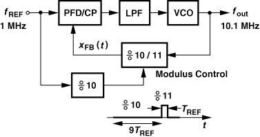
As an example, consider the circuit shown in Fig. 11.1, where fREF = 1 MHz and N = 10. Let us assume the prescaler divides by 10 for 90% of the time (nine reference cycles) and by 11 for 10% of the time (one reference cycle). Thus, for every 10 reference cycles, the output produces 9 × 10 + 11 = 101 pulses, yielding an average divide ratio of 10.1 and hence fout = 10.1 MHz. In principle, the architecture can provide arbitrarily fine frequency steps if the durations of the ÷N and ÷(N + 1) modes can be adjusted by small percentages.
Figure 11.1 Example of fractional-N loop.
The above example illustrates the efficacy of fractional-N synthesis with respect to creating fine channel spacings while running from a relatively high reference frequency. In addition to a wider loop bandwidth than that of integer-N architectures, this approach also reduces the in-band “amplification” of the reference phase noise (Chapter 10) because it requires a smaller N (≈ fout/fREF). (In the above example, an integer-N loop would multiply the reference phase noise by a factor of 100.)
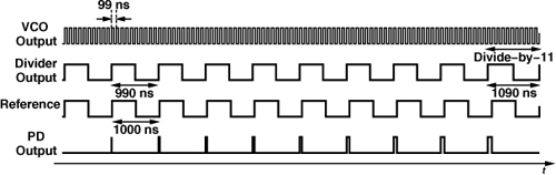
The principal challenge in the design of FNS’s stems from “fractional spurs.” To understand this effect, let us return to the loop of Fig. 11.1 and reexamine its operation in the time domain. If the circuit operates as desired, then the output period is constant and equal to (10.1 MHz)−1 ≈ 99 ns. Recall that, for nine reference cycles, this output period is multiplied by 10, and for one reference cycle, by 11. As shown in Fig. 11.2, each of the first nine cycles of the divided signal is 990 ns long, slightly shorter than the reference cycles. Consequently, the phase difference between the reference and the feedback signal grows in every period of fREF, until it returns to zero when divide-by-11 occurs.1 Thus, the phase detector generates progressively wider pulses, leading to a periodic waveform at the LPF output. Note that this waveform repeats every 10 reference cycles, modulating the VCO at a rate of 0.1 MHz and producing sidebands at ±0.1 MHz × n around 10.1 MHz, where n denotes the harmonic number. These sidebands are called fractional spurs. More generally, for a nominal output frequency of (N + α)fREF, the LPF output exhibits a repetitive waveform with a period of 1/(αfREF).
Figure 11.2 Detailed operation of fractional-N loop.
The appearance of fractional spurs can be explained from another perspective. Depicted in Fig. 11.3, the overall feedback signal, xFB(t) can be written as the sum of two waveforms, each of which repeats every 10,000 ns. The first waveform consists of nine periods of 990 ns and a “dead” time of 1090 ns, while the second is simply a pulse of width 1090/2 ns. Since each waveform repeats every 10,000 ns, its Fourier series consists of only harmonics at 0.1 MHz, 0.2 MHz, etc. If the phase detector is viewed as a mixer, we observe that the harmonics near 1 MHz are translated to “baseband” as they emerge from the PD, thus modulating the VCO.
Figure 11.3 Long periodicity in a fractional-N loop.

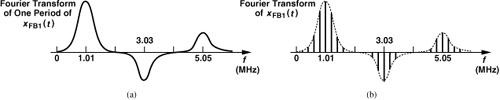
If the feedback signal is considered a 1-MHz waveform (while its fundamental frequency is in fact 0.1 MHz), then it contains many sidebands at integer multiples of 0.1 MHz. As explained in Chapter 3, the sidebands can be considered FM (and AM) components, leading to periodic phase modulation:
![]()
Comparing xFB(t) with an ideal reference at fREF, the PFD produces an output proportional to φ(t), driving the loop filter with a periodic waveform at 0.1 MHz. This perspective does not need to consider the PFD as a mixer.
In summary, the feedback signal in the above example has a period of 10 μs and hence harmonics at n × 0.1 MHz, but we roughly view it as a signal with an average frequency of 1 MHz and sidebands that are offset by ±0.1 MHz, etc. These sidebands yield components at n × 0.1 MHz at the PFD output, modulating the VCO and creating fractional spurs.
11.2 Randomization and Noise Shaping
The fractional spurs are quite large, requiring means of “compensation.” The field of fractional-N synthesizers has introduced hundreds of compensation techniques in the past several decades. A class of techniques that lends itself to integration in CMOS technology and has become popular employs “noise shaping” [1]. This chapter is dedicated to this class of FNS’s. We begin our study with the concepts of “modulus randomization” and noise shaping.
11.2.1 Modulus Randomization
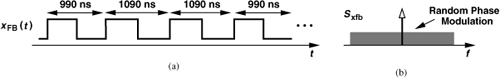
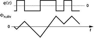
Our analysis of the synthesizer in Fig. 11.1 reveals a periodicity in the behavior of the loop given by 10 reference cycles (0.1 MHz). What happens if the divider modulus is randomly set to 10 or 11 but such that its average value is still 10.1? As shown in Fig. 11.5(a), xFB(t) exhibits a random sequence of 990-ns and 1090-ns periods. Thus, unlike the situation portrayed in Fig. 11.4(b), xFB(t) now contains random phase modulation [Fig. 11.5(b)],
![]()
leading to a random waveform (i.e., noise) at the PFD output. In other words, randomization of the modulus breaks the periodicity in the loop behavior, converting the deterministic sidebands to noise.
Figure 11.5 (a) Randomization of divide ratio, (b) effect on spectrum of feedback signal.
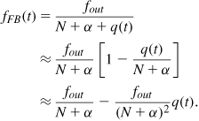
Let us now compute the noise, φn(t), in the feedback signal. Suppose the divider has two moduli, N and N + 1, and must provide an average modulus of N + α. We can write the instantaneous modulus as N + b(t), where b(t) randomly assumes a value of 0 or 1 and has an average value of α. The instantaneous frequency of the feedback signal is therefore expressed as
![]()
where fout denotes the VCO output frequency. In the ideal case, b(t) would be constant and equal to α, but our technique approximates α by a binary stream (i.e., with one-bit resolution), thereby introducing substantial noise. Since b(t) is a random variable with a nonzero mean, we may write it in terms of its mean and another random variable with a zero mean:
![]()
We call q(t) the “quantization noise” because it denotes the error incurred by b(t) in approximating the value of α. In Problem 11.1, we apply this result to the example in Fig. 11.1 with N = 10, α = 0.1 but without randomization of b(t).
Solution:
Figure 11.6 (a) Random binary waveform having an average value of α, (b) quantization noise waveform.

If q(t) ![]() N + α, we have
N + α, we have
The feedback waveform arriving at the PFD is thus expressed as
![]()
because the phase is given by the time integral of the frequency. As expected, the divider output has an average frequency of fout/(N + α) and a phase noise given by
![]()
In Problem 11.2, we compute this phase for the example in Fig. 11.1.
Using the above results, we now determine the synthesizer output phase noise within the loop bandwidth. Viewing the phase noise as a component in the reference, we simply multiply Eq. (11.10) by the square of the average divide ratio, N + α:
![]()
Alternatively, since fout = (N + α)fREF,
![]()
11.2.2 Basic Noise Shaping
While suppressing the fractional spurs, modulus randomization gives rise to a high phase noise. The high quantization noise arises from approximating a precise value, α, by only two coarse levels, namely, 0 and 1. Since the prescaler modulus cannot assume any other value between N and N + 1, the resolution is limited to 1 bit, and the quantization noise cannot be reduced directly. Modern FNS’s cope with this issue by performing the randomization such that the resulting phase noise exhibits a high-pass spectrum. Illustrated in Fig. 11.9, the idea is to minimize the spectral density near the center frequency of the feedback signal and allow the limited synthesizer loop bandwidth to suppress the noise farther away from the center frequency. The generation of the sequence b(t) so as to create a high-pass phase spectrum is called “noise shaping.”
Figure 11.9 Synthesizer employing modulus randomization.
Let us summarize our thoughts. We wish to generate a random binary sequence, b(t), that switches the divider modulus between N and N + 1 such that (1) the average value of the sequence is α, and (2) the noise of the sequence exhibits a high-pass spectrum. The first goal is fulfilled if the number of ONEs divided by the number of ONEs and ZEROs is equal to α (over a long duration). We now focus on the second goal.
In our first step toward understanding the concept of noise shaping, we consider the negative feedback system shown in Fig. 11.10, where X(s) denotes the main input and Q(s) a secondary input, e.g., additive noise. The transfer function from Q(s) to Y(s) [with X(s) set to zero] is equal to
![]()
Figure 11.10 Feedback system with noise injected near the output.
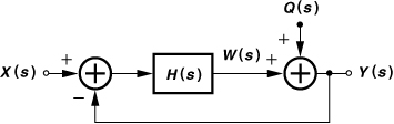
For example, if H(s) is an ideal integrator,
![]()
In other words, a negative feedback loop containing an integrator acts as a high-pass system on the noise injected “near” the output. The reader may recognize the similarity of this behavior to the effect of VCO phase noise in PLLs (Chapter 9). If Q varies slowly with time, then the loop gain is large, making W a close replica of Q and hence Y small. From another point of view, the integrator provides a high loop gain at low frequencies, forcing Y to be approximately equal to X. Note that these results remain valid whether the system is analog, digital, or a mixture of analog and digital blocks.
Solution:
![]()
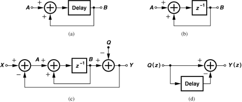
Figure 11.11 (a) Discrete-time integrator, (b) integrator z-domain model, (c) use of integrator in a feedback loop, (d) simplified diagram of the feedback loop.
![]()
![]()
The last point in the above example merits further investigation. Shown in Fig. 11.12 is a system that subtracts a delayed version of a(t) from a(t). The delay is equal to one clock cycle, Tck. Figure 11.12(a) depicts a case where a(t) changes significantly during one clock cycle, leading to an appreciable value for a2 − a1. That is, if a(t) changes slowly, g(t) ≈ 0. If the clock frequency increases [Fig. 11.12(b)], a(t) finds less time to change, and a1 and a2 exhibit a small difference (i.e., they are strongly correlated). The key result here is that the systems in Figs. 11.11(c) and (d) reject Q by a greater amount if the delay element is clocked faster.
Figure 11.12 Addition of a signal and its delayed version (a) for high and (b) low clock frequencies.

We now assemble the concepts described thus far and construct a system that produces a binary output with an average value of α and a shaped noise spectrum. As shown in Fig. 11.14, we begin with an m-bit representation of α that is sufficiently accurate (X in Fig. 11.13). This value is applied to a feedback loop derived from that in Fig. 11.11(c), except that the high-resolution output of the integrator drives a flipflop (i.e., a one-bit quantizer), thereby generating a single-bit binary stream at the output. The quantization from m + 2 bits to 1 bit introduces significant noise, but the feedback loop shapes this noise in proportion to 1 − z−1. As explained in Example 11.7, the high integrator gain ensures that the average of the output is equal to X. This feedback system is called a “ΣΔ modulator.” The choice of m in Fig. 11.14 is given by the accuracy with which the synthesizer output frequency must be defined. For example, for a frequency error of 10 ppm, m ≈ 17 bits.
Figure 11.14 ΣΔ modulator with one-bit output.

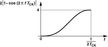
In the next step, we examine the shape of 1 − z−1 in the frequency domain. Recall from the definition of the z-transform that z = exp(j2πfTCK), where TCK denotes the sampling or clock period. Thus, in the systems of Figs. 11.11(c) and 11.13,
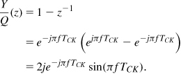
It follows that

Plotted in Fig. 11.15, the noise shaping function begins from zero at f = 0 and climbs to 4 at f = (2TCK)−1 (half the clock frequency). As predicted previously, a higher clock rate expands the function horizontally, thus reducing the noise density at low frequencies. The system of Fig. 11.14 is called a “first-order 1-bit ΣΔ modulator” because it contains one integrator.
Figure 11.15 Noise-shaping function in a first-order modulator.
What can we say about the shape of Sy(f)? From Eq. (11.14),
![]()
As explained below, the clock frequency, fCK, is in fact equal to the synthesizer reference frequency, fREF. Since the PLL bandwidth is much smaller than fREF, we can consider Sq(f) relatively flat for the frequency range of interest (Fig. 11.16). We hereafter assume that the shape of Sy(f) is approximately the same as that of the noise-shaping function.
Figure 11.16 Product of binary waveform quantization spectrum and noise-shaping function.
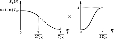
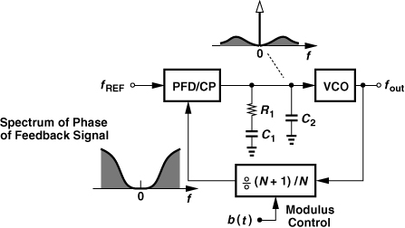
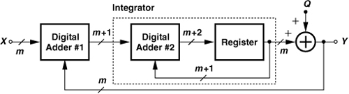
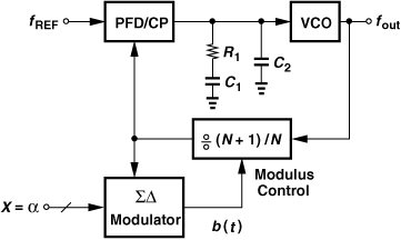
Figure 11.17 shows the fractional-N synthesizer developed thus far. Clocked by the feedback signal, the ΣΔ modulator toggles the divide ratio between N and N + 1 so that the average is equal to N + α.
Figure 11.17 Basic fractional-N loop using a ΣΔ modulator to randomize the divide ratio.
Problem of Tones
The output spectrum of ΣΔ modulators contains the shaped noise shown in Fig. 11.15, but also discrete tones. If lying at low frequencies, such tones are not removed by the PLL, thereby corrupting the synthesizer output.
To understand the origin of tones, we return to the modulator of Fig. 11.14 and ask, if X is constant, is the output binary sequence random? Since the system has no random inputs, we suspect that the output may not be random, either. For example, suppose X = 0.1. Then, as shown in Fig. 11.18, the output contains one pulse every ten clock cycles. In fact, after each output pulse, the integrator output falls to zero and subsequently rises in steps of 0.1 each clock cycle until it reaches 1 and drives the FF output high. In other words, the system exhibits a periodic behavior (“limit cycle”). Repeating every ten clock cycles, the output waveform of Fig. 11.18 consists of harmonics of fCK/10, some of which are likely to fall within the bandwidth of the PLL and hence appear as spurs at the output.
Figure 11.18 Generation of idle tones in a ΣΔ loop.

To suppress these tones, the periodicity of the system must be broken. For example, if the LSB of X randomly toggles between 0 and 1, then the pulses in the output waveform of Fig. 11.18 occur randomly, yielding a spectrum with relatively small tones (but a higher noise floor). Called “dithering,” this randomization must be performed at a certain rate: if excessively slow, it does not sufficiently break the periodicity. (Dithering may still produce tones in a nonlinear system.)
11.2.3 Higher-Order Noise Shaping
The noise shaping function expressed by Eq. (11.24) and illustrated in Fig. 11.15 does not adequately suppress the in-band noise. This can be seen by noting that, for f ![]() (π TCK)−1, Eq. (11.23) reduces to
(π TCK)−1, Eq. (11.23) reduces to
![]()
i.e., the spectrum has a second-order roll-off as f approaches zero.2 We therefore seek a system that exhibits a sharper roll-off, e.g., an output spectrum in proportion to fn with n > 2. The following development will call for a “non-delaying integrator,” shown in Fig. 11.19. The transfer function is given by
![]()
Figure 11.19 Non-delaying integrator.

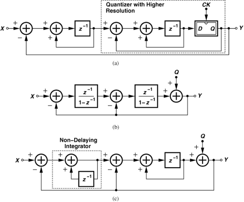
In order to arrive at a system with a higher-order noise shaping, let us revisit the system of Fig. 11.14 and seek to increase the resolution of the quantizer (the flipflop) itself, i.e., a quantizer that produces lower quantization noise. From the foregoing developments, we recognize that a ΣΔ modulator can serve such a purpose because it suppresses the quantization noise at low frequencies. We therefore replace the 1-bit quantizer with a ΣΔ modulator [Fig. 11.20(a)]. To determine the noise shaping function, we write from the equivalent model shown in Fig. 11.20(b),
![]()
Figure 11.20 (a) Use of a ΣΔ modulator as a quantizer within a ΣΔ loop, (b) simplified model of (a), (c) use of a non-delaying integrator.
It follows that
![]()
The numerator indeed represents a sharper shaping, but the denominator exhibits two poles. Modifying the first integrator to a non-delaying topology [Fig. 11.20(c)], we have
![]()
and hence
![]()
Following the derivations leading to Eq. (11.23), we have
![]()
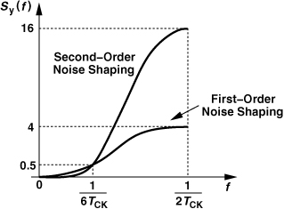
i.e., the noise shaping falls in proportion to f4 as f approaches zero. The system in Fig. 11.20(c) is called a “second-order 1-bit ΣΔ modulator.” Plotted in Fig. 11.21 are the noise shaping functions given by (11.23) and (11.32), revealing that the latter remains lower than the former for frequencies up to (6TCK)−1.
Figure 11.21 Noise shaping in first- and second-order modulators.
Is it possible to further raise the order of the ΣΔ modulator loop, thereby obtaining even sharper noise shaping functions? Yes, additional integrators in the loop provide a higher-order noise shaping. However, feedback loops containing more than two integrators are potentially unstable, requiring various stabilization techniques. Examples are described in [2].
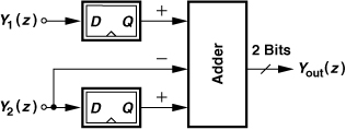
Another approach to high-order ΣΔ modulator design employs “cascaded loops.” Consider the first-order 1-bit loop shown in Fig. 11.22(a), where a subtractor finds the difference between the input and output of the quantizer, producing U = Y1 − W = Q, i.e., the quantization error introduced by the quantizer. We postulate that if this error is subtracted from Y1, the result contains a smaller amount of quantization noise. However, U has m bits. Thus, we must first convert it to a 1-bit representation with reasonable accuracy, a task well done by a ΣΔ modulator. As illustrated in Fig. 11.22(b), U drives a second loop, producing a 1-bit stream, Y2. Since the quantization error due to approximating the m-bit U by the 1-bit Y2 is shaped by the second loop, we observe that Y2 is a relatively accurate replica of U. Lastly, Y2 is combined with Y1, yielding Yout as a more accurate representation of X. This system is called a “1-1 cascade” to signify that each loop is of first order.
Figure 11.22 (a) Reconstruction of quantization noise, (b) cascaded modulators.

Let us compute the residual quantization noise present in Yout. Redrawing the system of Fig. 11.22(b) as shown in Fig. 11.23, where Q′ denotes the noise introduced by the second loop’s quantizer, we have
![]()
and
![]()
Figure 11.23 Cascaded modulators showing quantization noise components.

We wish to combine Y1(z) and Y2(z) such that Q(z) is cancelled. To this end, the “combiner” multiplies both sides of (11.33) by z−1 and both sides of (11.35) by (1 − z−1) and subtracts the latter result from the former:
![]()
Interestingly, the 1-1 cascade exhibits the same noise shaping behavior as the second-order modulator of Fig. 11.20(c).
Also known as the “MASH architecture,” cascaded modulators can achieve high-order noise shaping without the risk of instability inherent in high-order single-loop modulators. However, as illustrated by the above example, the final output of a cascade is more than one bit wide, dictating a multi-modulus divider. For example, if Yout assumes four possible levels, then a divider with moduli equal to N − 1, N, N + 1, and N + 2 is necessary. Examples of multi-modulus dividers are described in [3, 4].
11.2.4 Problem of Out-of-Band Noise
The trend illustrated in Fig. 11.21 makes it desirable to raise the order of noise shaping so as to lower the in-band quantization noise. Unfortunately, however, higher orders inevitably lead to a sharper rise in the quantization noise at higher frequencies, a serious issue because the noise spectrum is multiplied by only a second-order low-pass transfer function as it travels to the PLL output.
To investigate this point, recall from Eq. (11.7) that the shaped noise spectrum expressed by Eq. (11.32), for example, is in fact frequency noise (as it represents modulation of the divide ratio). To compute the phase noise spectrum, we return to the transfer function from the quantization noise to the frequency noise:
![]()
Now, since the phase noise, φ(z), is the time integral of the frequency noise, φ(z) = Y(z)/(1 − z−1),
![]()
The spectrum of the phase noise is thus obtained as
Appearing directly at one input of the phase detector, this phase noise spectrum is indistinguishable from the phase noise of the synthesizer reference, thus experiencing the low-pass transfer function of the PLL:
![]()
where N is the divider ratio and ω = 2πf. Illustrated in Fig. 11.25 are the noise-shaped spectrum and the PLL transfer function.3 If the ΣΔ modulator is clocked at a rate equal to the PLL reference (as is usually the case), then we note from Chapter 9 that f−3dB ≈ 0.1fREF ≈ 1/(10TCK). For small values of f, the noise shaping function in Eq. (11.42) can be approximated as ![]() , whereas the PLL transfer function is equal to N2. The product, Sout(f), therefore begins from zero and rises to some extent. For larger values of f, the f2 behavior of the noise shaping function cancels the roll-off of the PLL, leading to a relatively constant plateau. At values of f approaching 1/(2TCK) = fREF/2, the product is dominated by the PLL roll-off. If comparable with the shaped VCO phase noise, this peaking of the ΣΔ phase noise spectrum proves troublesome. Figure 11.26 summarizes the phase noise effects at the synthesizer output.
, whereas the PLL transfer function is equal to N2. The product, Sout(f), therefore begins from zero and rises to some extent. For larger values of f, the f2 behavior of the noise shaping function cancels the roll-off of the PLL, leading to a relatively constant plateau. At values of f approaching 1/(2TCK) = fREF/2, the product is dominated by the PLL roll-off. If comparable with the shaped VCO phase noise, this peaking of the ΣΔ phase noise spectrum proves troublesome. Figure 11.26 summarizes the phase noise effects at the synthesizer output.
Figure 11.25 Synthesizer output quantization noise.
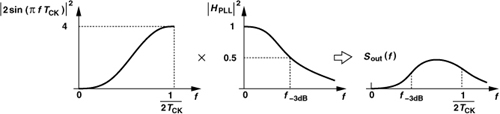
Figure 11.26 Phase noise effects at the output of a fractional-N loop.

The above study suggests that ΣΔ modulators having an order higher than 2 generate considerable phase noise at the synthesizer output unless the PLL bandwidth is reduced significantly, a trade-off violating the large bandwidth premise of fractional-N synthesizers. We quantify this behavior for a third-order modulator in Problem 11.4.
11.2.5 Effect of Charge Pump Mismatch
Our extensive study of PFD/CP nonidealities in Chapter 9 has revealed a multitude of effects that produce ripple on the control voltage of the oscillator and hence sidebands at the output. In particular, the mismatch between the Up and Down currents due to both
random effects and channel-length modulation proves quite serious in today’s designs. This mismatch creates additional issues in fractional-N synthesizers [5].
In order to understand the effect of charge pump mismatch, we consider the PFD/CP/LPF combination shown in Fig. 11.27(a) and study the net charge delivered to C1 as a function of the input phase difference, ΔTin [5]. Note that the current sources are called I1 and I2 and the current waveforms arriving at the output node, IUp and IDown. Also, Inet = IUp − IDown. Depicted in Fig. 11.27(b) are the waveforms for the case where A leads B by ΔTin seconds. The Up pulse goes high first, pumping a current of I1. The Down pulse goes high ΔTin seconds later, drawing a current of I2, and lasts ΔT1 seconds, where ΔT1 denotes the PFD reset pulsewidth (about five gate delays). The net current, Inet, thus assumes a value of I1 for ΔTin seconds and a value of I1 − I2 for ΔT1 seconds. Consequently, the total charge delivered to the loop filter is equal to
![]()
Figure 11.27 (a) PFD/CP with current mismatches, (b) effect for Up ahead of Down, (c) effect for Up behind Down, (d) resulting characteristic.
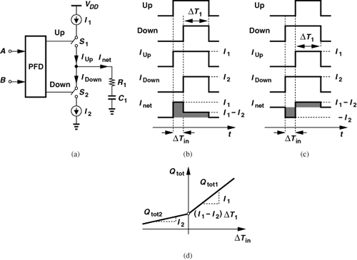
Now, let us reverse the polarity of the input phase difference. As shown in Fig. 11.27(c), the Down pulse goes high first, creating a net current of −I2 until the Up pulse goes high and Inet jumps to I1 − I2. In this case,
![]()
(Note that ΔTin is negative here.) The key observation here is that the slope of Qtot as a function of ΔTin jumps from I2 to I1 as ΔTin goes from negative values to positive values [Fig. 11.27(d)]. In other words, the PFD/CP characteristic suffers from nonlinearity. This nonlinearity adversely affects the broadband noise generated by the ΣΔ modulator and hence the feedback divider.
Solution:
Figure 11.28 Effect of current mismatch in an integer-N loop: (a) steady state, (b) random phase lead, (c) random phase lag, (d) resulting characteristic.
The nonlinearity depicted in Fig. 11.27(d) becomes critical in ΣΔ fractional-N synthesizers because the feedback divider output contains large, random phase excursions. Since the phase difference sensed by the PFD fluctuates between large positive and negative values, the charge delivered to the loop filter is randomly proportional to I1 or I2.
What is the effect of the above nonlinearity on a ΣΔ fractional-N synthesizer? Let us decompose the characteristic of Fig. 11.27(d) into two components: a straight line passing through the “end points” and a nonmonotonic “error” (Fig. 11.29).
Figure 11.29 Decomposition of characteristic to nonlinear and linear components.
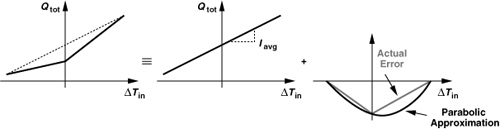
The end points correspond to the maximum negative and positive phase fluctuations that appear at the divider output. We roughly approximate the error by a parabola, ![]() , and write
, and write
![]()
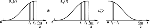
where Iavg denotes the slope of the straight line. We expect that the second term alters the spectrum of the ΣΔ phase noise. In fact, the multiplication of ΔTin (phase noise) by itself is a mixing effect and translates to the convolution of its spectrum with itself. We must therefore perform the convolution depicted in Fig. 11.30. Decomposing the spectrum into narrow channels and viewing each as an impulse, we note that the convolution of a channel centered at + f1 (and −f1) with another centered at + f2 (and −f2) results in a component at f2 − f1 and another at f2 + f1. Similarly, the convolution of a channel at f1 with another near zero yields one near f1 but with a small amount of energy. As shown in Fig. 11.30, the overall spectrum now exhibits a peak near zero frequency, falls to zero at fCK/2, and rises again to reach another peak at fCK. Of course, the height of each peak is proportional to a2 and hence relatively small, but possibly quite higher than the original shaped noise near zero frequency. That is, charge pump nonlinearity translates the ΣΔ modulator’s high-frequency quantization noise to in-band noise, thus modulating the VCO. We also note that this “noise folding” effect becomes more pronounced as the order of the ΣΔ modulator and hence the high-frequency quantization noise increase. Similar folding may also occur for the idle tones described in Section 11.2.2.
Figure 11.30 Downconversion of high-frequency quantization noise as a result of CP nonlinearity.
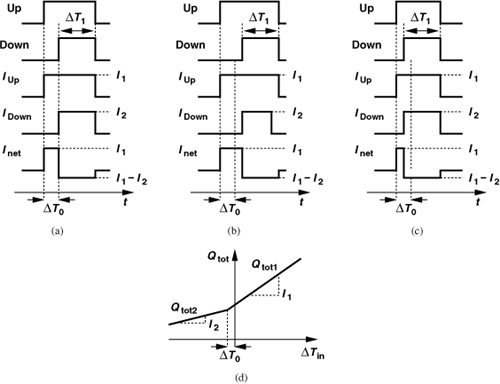
In order to alleviate the charge pump mismatch issue, we can consider some of the solutions studied in Chapter 9. For example, the topology of Fig. 9.53 suppresses both random and deterministic mismatches, but it requires an op amp with a nearly rail-to-rail input common-mode range. Alternatively, we can return to Example 11.9 and observe that the nonlinearity does not manifest itself so long as the static phase offset is greater than the phase fluctuations produced by the feedback divider. In other words, if a deliberate mismatch is introduced between the Up and Down currents so as to establish a large static phase offset, then the slope of the characteristic remains constant around zero. As shown in Fig. 11.28(d), a mismatch of ΔI = I1 − I2 affords a peak-to-peak phase fluctuation of
![]()
where I denotes the smaller of I1 and I2 and ΔT1, the width of the PFD reset pulses. Unfortunately, such a large mismatch also leads to a large ripple on the control voltage and a higher charge pump noise (because the CP current flows for a longer time).
Another approach to creating a static phase error splits the PFD reset pulse as depicted in Fig. 11.31(a) [6]. Since FF1 is reset later than FF2 by an amount equal to TD, the Up pulse falls TD seconds later than the Down pulse. The PLL must lock with a zero net charge, thus settling such that
![]()
Figure 11.31 Split reset pulses in a PFD to avoid slope change.
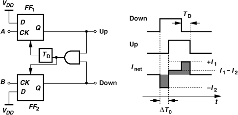
The static phase offset is now given by
![]()
That is, for a sufficiently large TD and hence ΔT0, phase fluctuations simply modulate the width of the negative current pulse in Inet, leading to a characteristic with a slope of I2. Unfortunately, this technique also introduces significant ripple (a peak voltage of I2 ΔT0) on the control voltage.
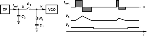
The above two approaches cope with the charge pump mismatch problem while producing ripple on the control voltage. Fortunately, as mentioned in Chapter 10, a sampling circuit interposed between the charge pump and the loop filter can “mask” the ripple, ensuring that the oscillator control line sees only the settled voltage produced by the CP (Fig. 11.32). In other words, a deliberate current offset or Up/Down misalignment along with a sampling circuit removes the nonlinearity resulting from the charge pump and yields a small ripple.
Figure 11.32 Sampling filter to mask the control voltage from charge pump activity.
11.3 Quantization Noise Reduction Techniques
As explained in Section 11.2.4, the sharp rise in the quantization noise of ΣΔ modulators leads to substantial phase noise at the output of fractional-N synthesizers. In fact, this phase noise contribution can well exceed that of the VCO itself. This issue is ameliorated by reducing the PLL bandwidth, but at the cost of the advantages envisioned for fractional-N operation, namely, fast settling and suppression of the VCO phase noise across a large bandwidth. In this section, we study a number of techniques that lower the ΣΔ modulator phase noise contribution without reducing the synthesizer’s loop bandwidth.
11.3.1 DAC Feedforward
Let us begin by reconstructing the quantization noise of the ΣΔ modulator. Figure 11.33 illustrates an example where a first-order, one-bit modulator produces
![]()
Figure 11.33 Reconstruction of quantization noise.
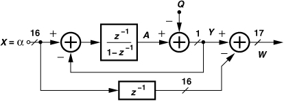
We then delay X(z) by one clock cycle and subtract the result from Y(z) to reconstruct the quantization error:
![]()
This operation yields the total (shaped) quantization error present in Y(z). Note that, in this example, W(z) has a 17-bit representation.
The reader must not confuse this operation with the quantization error reconstruction in cascaded modulators. Here, W is the shaped noise, whereas in cascaded modulators, we computed Q = Y − A, which is unshaped.
What can be done with the reconstructed error? Ideally, we wish to subtract W(z) from Y(z) to “clean up” the latter. However, such a subtraction would simply yield X = α with a 16-bit word length! We must therefore seek another point in the system where W(z) can be subtracted from Y(z), but not lead to a multi-bit digital signal.
Following the above line of thought, suppose, as shown in Fig. 11.34(a), we convert W(z) to analog charge and inject the result into the loop filter with a polarity that cancels the effect of the (1 − z−1)Q(z) noise arriving from the ΣΔ modulator. In the absence of analog and timing mismatches, each ΣΔ modulator output pulse traveling through the divider, the PFD, and the charge pump is met by another pulse produced by the DAC, facing perfect cancellation. We call this method “DAC feedforward cancellation.”
Figure 11.34 (a) Basic DAC feedforward, (b) use of integrator in DAC path, (c) use of second modulator to relax required DAC resolution.
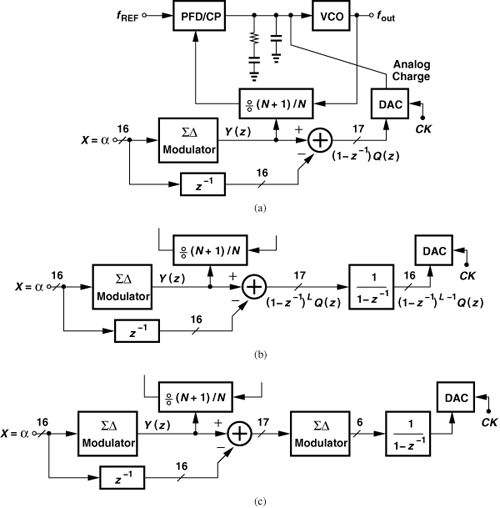
The system of Fig. 11.34(a) entails a number of issues, requiring some modifications. First, we note that the PFD/CP combination generates a charge proportional to the phase of the divider output, i.e., the time integral of the frequency. Thus, the quantization noise arriving at the loop filter is of the form (1 − z−1)Q(z)/(1 − z−1) = Q(z), whereas the DAC output is of the form (1 − z−1)Q(z). We must then interpose an integrator between the subtractor and the DAC. Figure 11.34(b) illustrates the result with a more general ΣΔ modulator of order L.
The second issue relates to the accuracy required of the DAC. Since it is extremely difficult to realize a 17-bit DAC, we may be tempted to truncate the DAC input to, say, 6 bits, but the truncation folds the high-frequency quantization noise to low frequencies [5] in a manner similar to the convolution shown in Fig. 11.30. It is thus necessary to “requantize” the 17-bit representation by another ΣΔ modulator, thereby generating a, say, 6-bit representation whose quantization noise is shaped [5] [Fig. 11.34(c)].
The third issue arises from the nature of the pulses travelling through the two paths. The Up and Down pulses activate the CP for only a fraction of the reference period, producing a current pulse of constant height each time. The DAC, on the other hand, generates current pulses of constant width. As shown in Fig. 11.35, the areas under the CP and DAC pulses are equal in the ideal case, but their arrival times and durations are not. Consequently, some ripple still appears on the control voltage. For this reason, the sampling loop filter of Fig. 11.32 is typically used to mask the ripple.
Figure 11.35 CP and DAC output current waveforms.

The mismatch studied in the above example is also called the “DAC gain error.” Figure 11.36(a) conceptually shows a 3-bit DAC whose output current is given by
![]()
where D3D2D1 represents the binary input. Figure 11.36(b) plots the input/output characteristic, revealing that an error in IREF translates to an error in the slope, i.e., a gain error. Since both the charge pump current and the DAC current are defined by means of current mirrors, mismatches between these mirrors lead to incomplete cancellation of the quantization noise. Methods of DAC gain calibration are described in [7].
Figure 11.36 (a) Current-mode DAC implementation, (b) input/output characteristic.
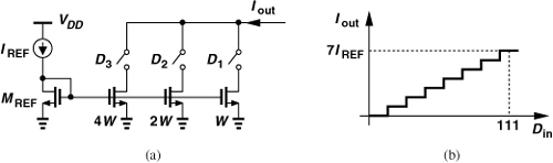
How should the full-scale current of the DAC (e.g., 7IREF in the above example) be chosen? The tallest pulse generated by the DAC must cancel the widest pulse produced by the CP, which in turn is given by the largest phase step at the output of the feedback divider. Interestingly, the maximum divider phase step depends on the order of the ΣΔ modulator, reaching three VCO cycles for an order of two and seven for an order of three. The DAC full scale is set accordingly.
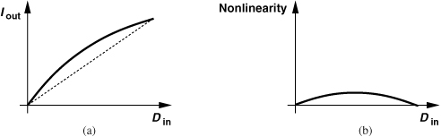
In the feedforward approach described above, the DAC resolution need not exceed 5 or 6 bits, but its linearity must be quite higher [5]. Suppose, as shown in Fig. 11.37(a), the DAC characteristic exhibits some nonlinearity. Finding the difference between this characteristic and the straight line passing through the end points, we obtain the nonlinearity profile depicted in Fig. 11.37(b). In a manner similar to the study of charge pump nonlinearity in Section 11.2.5, we can approximate this profile by a polynomial, concluding that the DAC input is raised to powers of 2, 3, etc. As a result, the shaped high-frequency components of the quantization noise applied to the DAC are convolved and folded to low frequencies, raising the in-band phase noise (Fig. 11.30). For this reason, the DAC must employ additional measures to achieve a high linearity [5].
Figure 11.37 (a) DAC characteristic and (b) nonlinearity profile.
11.3.2 Fractional Divider
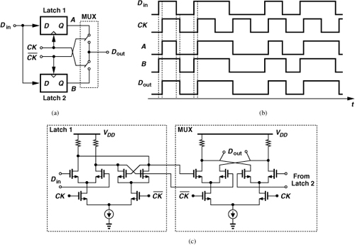
Another approach to reducing the ΣΔ modulator quantization noise employs “fractional” dividers, i.e., circuits that can divide the input frequency by noninteger values such as 1.5 or 2.5. For example, if a circuit can divide by 2 or 2.5, then the quantization error is halved, exhibiting a spectrum that is shifted down by 6 dB.4 But how can a circuit divide by, say, 1.5? The key to this operation is the notion of “double-edge-triggered” (DET) flipflops. Illustrated in Fig. 11.38(a), a DET flipflop incorporates two D latches driven by CK and ![]() and a multiplexer (MUX). When CK is high, the top latch is in the sense mode and the bottom latch in the hold mode, and vice versa. Also, the MUX selects A when CK is low and B when it is high.5 Let us now drive the circuit with a “half-rate clock,” i.e., one whose period is twice the input bit period. Thus, as depicted in Fig. 11.38(b), even with a half-rate clock, Dout tracks Din. In other words, for a given clock rate, the input data to a DET flipflop can be twice as fast as that applied to a single-edge-triggered counterpart. Figure 11.38(c) shows a CML realization of the circuit.
and a multiplexer (MUX). When CK is high, the top latch is in the sense mode and the bottom latch in the hold mode, and vice versa. Also, the MUX selects A when CK is low and B when it is high.5 Let us now drive the circuit with a “half-rate clock,” i.e., one whose period is twice the input bit period. Thus, as depicted in Fig. 11.38(b), even with a half-rate clock, Dout tracks Din. In other words, for a given clock rate, the input data to a DET flipflop can be twice as fast as that applied to a single-edge-triggered counterpart. Figure 11.38(c) shows a CML realization of the circuit.
Figure 11.38 (a) Double-edge-triggered flipflop, (b) input and output waveforms, (c) CML implementation.
Let us now return to the ÷3 circuit studied in Chapter 9 and replace the flipflops with the DET circuit of Fig. 11.39(a).6 Noting that each FF now “reads” its input both when CK is high and when it is low, we begin with ![]() and observe that the first high clock level maintains Q1 at ZERO (because
and observe that the first high clock level maintains Q1 at ZERO (because ![]() was ZERO) and raises
was ZERO) and raises ![]() to ONE (because Q1 was ZERO) [Fig. 11.39(b)]. When CK falls, the flipflops read their inputs again, producing Q1 = 1 and
to ONE (because Q1 was ZERO) [Fig. 11.39(b)]. When CK falls, the flipflops read their inputs again, producing Q1 = 1 and ![]() . Finally, when CK goes high again, Q1 remains high while
. Finally, when CK goes high again, Q1 remains high while ![]() falls. The circuit therefore produces one output period for every 1.5 input periods.
falls. The circuit therefore produces one output period for every 1.5 input periods.
Figure 11.39 (a) Divide-by-1.5 circuit, (b) input and output waveforms.

DET flipflops can be used in other dividers having an odd modulus to obtain a fractional divide ratio. For example, a ÷5 circuit is readily transformed to a ÷2.5 stage. Note, however, that DET flipflops suffer from a larger clock input capacitance than their single-edge-triggered counterparts. Also, clock duty cycle distortion leads to unwanted spurs at the output.
11.3.3 Reference Doubling
Our derivation of the noise shaping function in Section 11.2.2 indicates a direct dependence on the clock frequency. In fact, Eq. (11.26) suggests that if TCK is halved, the noise power falls by 6 dB, making it desirable to use the highest available reference frequency. Generated by a crystal oscillator, the reference frequency is typically limited to less than 100 MHz, especially if power consumption, phase noise, and cost are critical. We then surmise that if the reference frequency can be doubled by means of an on-chip circuit preceding the PLL, then the phase noise due to the ΣΔ modulator quantization can be reduced by 6 dB (for a first-order loop) [8].
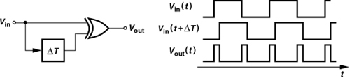
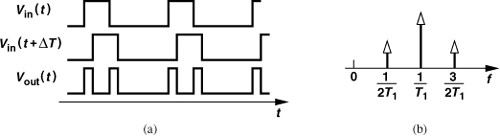
Figure 11.40 shows a frequency doubler circuit: the input is delayed and XORed with itself, producing an output pulse each time Vin(t) and Vin(t − ΔT) are unequal.
Figure 11.40 Frequency doubler.

Unfortunately, the circuit of Fig. 11.40 produces unevenly-spaced pulses if the input duty cycle deviates from 50% [Fig. 11.42(a)]. Following the above example [8], we decompose the output into two waveforms having a period of 2T1 and recognize that the time shift between V1(t) and V2(t), ΔT, now deviates from T1. Thus, the odd harmonics are not completely cancelled, appearing as sidebands around the main component at 1/T1 [Fig. 11.42(b)]. Since the PLL bandwidth is chosen about one-tenth of 1/T1, the sidebands are attenuated to some extent. We prove in Problem 11.10 that a loop bandwidth of 2.5ωn = 0.1 × (2π/T1) lowers the magnitude of the sidebands at 1/(2T1) by about 16 dB. However, while traveling to the synthesizer output, the sidebands grow by a factor equal to the feedback divide ratio.
Figure 11.42 (a) Doubler output in the presence of input duty cycle distortion, (b) resulting spectrum.
The foregoing analysis reveals that the duty cycle of the input waveform must be tightly controlled. The synthesizer described in [8] employs a duty cycle correction circuit. Such circuits still suffer from residual duty cycle errors due to their internal mismatches, possibly yielding unacceptably large reference sidebands at the synthesizer output—unless the loop bandwidth is reduced.
11.3.4 Multiphase Frequency Division
It is possible to reduce the quantization error in the divide ratio through the use of multiple phases of the VCO. From our analysis in Section 11.1, we note that when the divider modulus switches from N to N + 1 (or vice versa), the divider output phase jumps by one VCO period (Fig. 11.43). On the other hand, if finer phases of the VCO are available, the phase jumps can become proportionally smaller, resulting in lower quantization noise.
Figure 11.43 Phase jumps at the output of dual-modulus divider.
It is possible to create a fractional divide ratio by means of a multiphase VCO and a multiplexer. Suppose a VCO generates M output phases with a minimum spacing of 2π/M, and the MUX selects one phase each time, producing an output given by
![]()
where k is an integer. Now, let us assume that k varies linearly with time, sequencing through 0, 1, ..., M − 1, M, M + 1, .... Thus, k = βt, where β denotes the rate of change of k, and hence
![]()
revealing a frequency of ωc−β(2π/M). The divide ratio is therefore equal to 1−(β/ωc)(2π/M).
As an example, consider the circuit shown in Fig. 11.44(a), where the quadrature phases of a VCO are multiplexed to generate an output. Initially, VI is selected and Vout tracks VI until t = t1, at which point, VQ is selected. Similarly, Vout tracks VQ until t = t2, and then ![]() until t = t3, etc. We therefore observe that this periodic “stitching” of the quadrature phases yields an output with a period of Tin + Tin/4 = 5Tin/4, equivalently, a ÷1.25 operation. In other words, this technique affords a frequency divider having a modulus of 1 and a modulus of 1.25 [10]. Since the divide ratio can be adjusted in a step of 0.25, the quantization noise falls by 20 log 4 = 12 dB [10].
until t = t3, etc. We therefore observe that this periodic “stitching” of the quadrature phases yields an output with a period of Tin + Tin/4 = 5Tin/4, equivalently, a ÷1.25 operation. In other words, this technique affords a frequency divider having a modulus of 1 and a modulus of 1.25 [10]. Since the divide ratio can be adjusted in a step of 0.25, the quantization noise falls by 20 log 4 = 12 dB [10].
Figure 11.44 (a) Multiplexed VCO phases, (b) waveforms showing divide-by-1.25 operation.

The use of quadrature LO phases in the above example does not pose additional constraints on the system because direct-conversion transceivers require such phases for upconversion and downconversion anyway. However, finer fractional increments necessitate additional LO phases, making the oscillator design more complex and power-hungry.
Multiphase fractional division must deal with two issues. First, the MUX select command (which determines the phase added to the carrier each time) is difficult to generate. This is because, to avoid glitches at the MUX output, this command must change only when none of the MUX inputs is changing. Viewing the MUX in Fig. 11.44(a) as four differential pairs whose output nodes are shared and whose tail currents are sequentially enabled, we draw the input and select waveforms of the ÷1.25 circuit as shown in Fig. 11.45. Note that the edges of the select waveforms have a small margin with respect to the input edges. Moreover, if the divide ratio must switch from 1.25 to 1, a different set of select waveforms must be applied, complicating the generation and routing of the select logic.
Figure 11.45 Problem of phase selection timing margin.

The second issue in multiphase fractional dividers relates to phase mismatches. In the circuit of Fig. 11.44(a), for example, the quadrature LO phases and the paths within the MUX suffer from mismatches, thereby displacing the output transitions from their ideal points in time. As shown in Fig. 11.46(a), the consecutive periods are now unequal. Strictly speaking, we note that the waveform now repeats every 4 × 1.25Tin = 5Tin seconds, exhibiting harmonics at 1/(5Tin). That is, the spectrum contains a large component at 4/(5Tin) and “sidebands” at other integer multiples of 1/(5Tin) [Fig. 11.46(b)].
Figure 11.46 (a) Effect of phase mismatches in VCO multiplexing, (b) resulting spectrum.

It is possible to randomize the selection of the phases in Fig. 11.44(a) so as to convert the sidebands to noise [10]. In fact, this randomization can incorporate noise shaping, leading to the architecture shown in Fig. 11.47. However, the first issue, namely, tight timing still remains. To relax this issue, the multiplexing of the VCO phases can be placed after the feedback divider [9, 10].
Figure 11.47 Use of a ΣΔ modulator to randomize selection of the VCO phases.

11.4 Appendix I: Spectrum of Quantization Noise
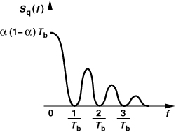
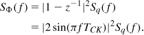
The random binary sequence, b(t), in Fig. 11.6(a) consists of square pulses of width Tb that randomly repeat at a rate of 1/Tb. In general, if a pulse p(t) is randomly repeated every Tb seconds, the resulting spectrum is given by [11]:

where σ2 denotes the variance (power) of the data pulses, P(f) the Fourier transform of p(t), and m the mean amplitude of the data pulses. In our case, p(t) is simply a square pulse toggling between 0 and 1 but with unequal probabilities: the probability that p(t) occurs is the desired average, α (= m). The variance of a random variable x is obtained as
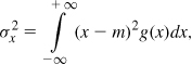
where g(x) is the probability density function of x. For b(t), g(x) consists of an impulse of height 1 − α at 0 and another height of α at 1 (why?) (Fig. 11.48). Thus,

Figure 11.48 Probability density function of binary data with an average value of α.

Also, the Fourier transform of p(t) is equal to
![]()
falling to zero at f = k/Tb for k ≠ 0. Thus, the second term in Eq. (11.57) reduces to (α2/Tb)2|P(0)|2δ(f) = α2δ(f ). These derivations lead to Eq. (11.13).
References
[1] T. A. D. Riley, M. A. Copeland, and T. A. Kwasniewski, “Delta-Sigma Modulation in Fractional-N Frequency Synthesis,” IEEE J. Solid-State Circuits, vol. 28, pp. 553–559, May 1993.
[2] R. Schreier and G. C. Temes, Understanding Delta-Sigma Data Converters, New York: Wiley, 2004.
[3] P. Larsson, “High-Speed Architecture for a Programmable Frequency Divider and a Dual-Modulus Prescaler,” IEEE J. Solid-State Circuits, vol. 31, pp. 744–748, May 1996.
[4] C. S. Vaucher et al., “A Family of Low-Power Truly Modular Programmable Dividers in Standard 0.35-μm CMOS Technology,” IEEE J. Solid-State Circuits, vol. 35, pp. 1039–1045, July 2000.
[5] S. Pamarti, L. Jansson, and I. Galton, “A Wideband 2.4 GHz Delta-Sigma Fractional-N PLL with 1 Mb/s In-Loop Modulation,” IEEE J. of Solid State Circuits, vol. 39, pp. 49–62, January 2004.
[6] S. E. Meninger and M. H. Perrott, “A 1-MHz Bandwidth 3.6-GHz 0.18-μm CMOS Fractional-N Synthesizer Utilizing a Hybrid PFD/DAC Structure for Reduced Broadband Phase Noise,” IEEE J. Solid-State Circuits, vol. 41, pp. 966–981, April 2006.
[7] M. Gupta and B.-S. Song, “A 1.8-GHz Spur-Cancelled Fractional-N Frequency Synthesizer with LMS-Based DAC Gain Calibration,” IEEE J. Solid-State Circuits, ISSCC Dig. Tech. Papers, pp. 323–324, Feb. 2006.
[8] H. Huh et al., “A CMOS Dual-Band Fractional-N Synthesizer with Reference Doubler and Compensated Charge Pump,” ISSCC Dig. Tech. Papers, pp. 186–187, Feb. 2004.
[9] C.-H. Park, O. Kim, and B. Kim, “A 1.8-GHz Self-Calibrated Phase-Locked Loop with Precise I/Q Matching,” IEEE J. Solid-State Circuits, vol. 36, pp. 777–783, May 2001.
[10] C.-H. Heng and B.-S. Song, “A 1.8-GHz CMOS Fractional-N Frequency Synthesizer with Randomized Multiphase VCO,” IEEE J. Solid-State Circuits, vol. 38, pp. 848–854, June 2003.
[11] L. W. Couch, Digital and Analog Communication Systems, Fourth Edition, New York: Macmillan Co., 1993.
Problems
11.1. In the circuit of Fig. 11.1, N = 10, and b(t) is a periodic waveform with α = 0.1. Determine the spectrum of fFB(t) ≈ (fout/N) [1 − b(t)/N]. Also, plot q(t).
11.2. Based on the results from the previous problem, express the output phase of the divider as a function of time.
11.3. Suppose in Eq. (11.14), Tb is equal to the PLL input reference period. Recall that the loop bandwidth is about one-tenth of the reference frequency. What does this imply about the critical part of Sq(f )?
11.4. Extend the analysis leading to Eq. (11.42) for a third-order ΣΔ modulator and study the problem of out-of-band noise in this case.
11.5. Determine the noise-shaping function for a fourth-order ΣΔ modulator and compare its peak with that of a second-order modulator. For a given PLL bandwidth, how many more decibels of phase noise peaking does a fourth-order modulator create than a second-order counterpart?
11.6. Extend the approach illustrated in Fig. 11.22(b) to a cascade of a second-order system and a first-order system. Determine the logical operation of the output combiner.
11.7. Suppose the Up and Down currents incur a 5% mismatch. Estimate the value of a in Eq. (11.45).
11.8. Determine whether two other effects in the PFD/CP combination result in noise folding: (a) unequal Up and Down pulsewidths, and (b) charge injection mismatch between the Up and Down switches in the charge pump.
11.9. Analyze the circuit of Fig. 11.38(a) if the MUX is driven by CK rather than ![]() .
.
11.10. Show that the sideband at 1/(2T1) in Fig. 11.42(b) is attenuated by approximately 16 dB in a PLL having fout = fin. What happens to the sideband magnitude if fout = Nfin? (Assume ζ and ωn remain unchanged.)