
Chapter 12. Power Amplifiers
Power amplifiers are the most power-hungry building block of RF transceivers and pose difficult design challenges. In the past ten years, the design of PAs has evolved considerably, drawing upon relatively complex transmitter architectures to improve the trade-off between linearity and efficiency. This chapter describes the analysis and design of PAs with particular attention to the limitations that they impose on the transmitter chain. A thorough treatment of PAs would require a book of its own, but our objective here is to lay the foundation. The reader is referred to [1, 2] for further details. The chapter outline is shown below.

12.1 General Considerations
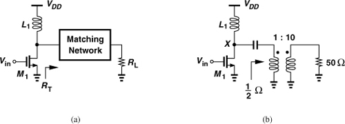
As the first step in our study, we consider a transmitter delivering 1 W (+30 dBm) of power to a 50-Ω antenna. The peak-to-peak voltage swing, Vpp, at the antenna reaches 20 V and the peak current through the load, 200 mA. For a common-source (or common-emitter) stage to drive the load directly, the configurations shown in Figs. 12.1(a) and (b) require a supply voltage greater than Vpp. However, if the load is realized as an inductor [Fig. 12.1(c)], the drain ac voltage exceeds VDD, even reaching 2VDD (or higher). While allowing a lower supply voltage, the inductive load does not relax the “stress” on the transistor; the maximum drain-source voltage experienced by M1 is still at least 20 V (10 V above VDD = 10 V) if the stage must deliver 1 W to a 50-Ω load.
Figure 12.1 CS stages with (a) resistive, (b) current source, and (c) inductive load.

The above example illustrates a fundamental issue in PA design, namely, the trade-off between the output power and the voltage swing experienced by the output transistor. It can be proven that the product of the breakdown voltage and fT of silicon devices is around 200 GHz · V [3]. Thus, transistors with an fT of 200 GHz dictate a voltage swing of less than 1 V.
Solution:
Figure 12.2 Output voltage waveform in a CS stage (a) when current flows from inductor to RL, (b) when current flows from RL to transistor.

In order to reduce the peak voltage experienced by the output transistor, a “matching network” is interposed between the PA and the load [Fig. 12.3(a)]. This network transforms the load resistance to a lower value, RT, so that smaller voltage swings still deliver the required power.
Figure 12.3 (a) Impedance transformation by a matching network, (b) realization by a transformer.
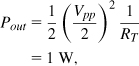
The need for transforming the voltage swings means that the current generated by the output transistor must be proportionally higher. In the above example, the peak current in the primary of the transformer reaches 10 × 200 mA = 2 A. Transistor M1 must sink both the inductor current and the peak load current, i.e., 4 A!
12.1.1 Effect of High Currents
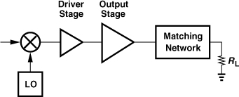
The enormous currents flowing through the output device and the matching network are one of the difficulties in the design of power amplifiers and the package. If the output transistor is chosen wide enough to carry a large current, then its input capacitance is very large, making the design of the preceding stage difficult. As depicted in Fig. 12.5, we may deal with this issue by interposing a number of tapered stages between the upconversion mixer(s) and the output stage. However, as explained in Chapter 4, the multiple stages tend to limit the TX output compression point. Moreover, the power consumed by the driver stages may not be negligible with respect to that of the output stage.
Figure 12.5 Tapering in a TX chain.
Another issue arising from the high ac currents in PAs relates to the package parasitics. The following example illustrates this point.
What is the effect of package parasitics? The inductance in series with the source degenerates the transistor, thereby lowering the output power. Moreover, ground and supply inductances may create feedback from the output to the input of the PA chain, causing ripple in the frequency response and even instability.
The large currents can also lead to a high loss in the matching network. The devices comprising this network—especially the inductors—suffer from parasitic resistances, thus converting the signal energy to heat. For this reason, the matching network for high-power applications is typically realized with off-chip low-loss components.
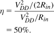
12.1.2 Efficiency
Since PAs are the most power-hungry block in RF transceivers, their efficiency is critical. A 1-W PA with 50% efficiency draws 2 W from the battery—much more than the rest of the transceiver does.
The efficiency of the PAs is defined by two metrics. The “drain efficiency” (for FET implementations) or “collector efficiency” (for bipolar implementations) is defined as
![]()
where PL denotes the average power delivered to the load and Psupp the average power drawn from the supply voltage. In some cases, the output stage may have a relatively low power gain, e.g., 3 dB, requiring a high input power. A quantity embodying this effect is the “power-added efficiency” (PAE), defined as
![]()
where Pin is the average input power.
12.1.3 Linearity
As explained in Chapter 3, the linearity of PAs becomes critical for some modulation schemes. In particular, PA nonlinearity leads to two effects: (1) high adjacent channel power as a result of spectral regrowth, and (2) amplitude compression. For example, QPSK modulation with baseband pulse shaping may suffer from the former and 16QAM from the latter. In some cases, AM/PM conversion may also be problematic.
The PA nonlinearity must be characterized with respect to the modulation scheme of interest. However, circuit-level simulations with actual modulated inputs take a very long time if they must produce an output spectrum that accurately reveals the ACPR (Chapter 3). Similarly, circuit-level simulations that quantify the effect of amplitude compression (i.e., the bit error rate) prove very cumbersome. For this reason, the PA characterization begins with two generic tests of nonlinearity based on unmodulated tones: intermodulation and compression. If employing two sufficiently large tones, the former provides some indication of ACPR. The amplitude of the tones is chosen such that each main component at the output is 6 dB below the full power level, thus producing the maximum desired output voltage swing when the two tones add in-phase [Fig. 12.6(a)]. For compression, a single tone is applied and its amplitude gradually increases so as to determine the output 1-dB compression point [Fig. 12.6(b)].
Figure 12.6 PA characterization by (a) two-tone test, (b) compression.

The above tests yield a first-order estimate of the PA nonlinearity. However, a more rigorous characterization is eventually necessary. Since the PA contains many storage elements, its nonlinearity cannot be simply expressed as a polynomial. As explained in Chapter 2, a Volterra series can represent dynamic nonlinearities, but it tends to be rather complex. An alternative approach models the nonlinearity as follows [4]. Suppose the modulated input is of the form
![]()
Then, the output also contains amplitude and phase modulation and can be written as
![]()
We now make a “quasi-static” approximation. If the input signal bandwidth is much less than the PA bandwidth, i.e., if the PA can follow the signal dynamics closely, then we can assume that both A(t) and Θ(t) are nonlinear static functions of only the input amplitude, a(t). That is,
![]()
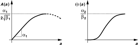
where A[a(t)] and Θ[a(t)] represent “AM/AM conversion” and “AM/PM conversion,” respectively [4]. For example, A and Θ are found to satisfy the following empirical equations:
![]()
![]()
where αj and βj are fitting parameters [4]. Illustrated in Fig. 12.7(a), A(a) is similar to the characteristic shown in Fig. 12.6(b) (but declines for high input levels). The AM/PM conversion function can also be obtained relatively easily by applying a tone at the PA input and measuring the PA phase shift as a function of the input amplitude.
Figure 12.7 Characteristics for AM/AM and AM/PM conversion.
The reader may wonder why the foregoing model is valid. Indeed, no analytical proof appears to have been offered to justify this model. Nonetheless, it has been experimentally verified that the model provides reasonable accuracy if the input signal bandwidth remains much smaller than the PA bandwidth. Note that for a cascade of stages, the overall model may be quite complex and the behavior of A and Θ quite different.
With A(a) and Θ(a) obtained from circuit simulations, the PA can be modeled by Eq. (12.11) and studied in a more efficient behavioral simulator, e.g., MATLAB. Thus, the effect of the PA nonlinearity on ACPR or the quality of signals such as OFDM waveforms can be quantified.
Another PA nonlinearity representation, called the “Rapp model” [5], is expressed as follows:

where α denotes the small-signal gain around Vin = 0, and V0 and m are fitting parameters. Dealing with only static nonlinearity, this model has become popular in integrated PA design. We return to this model in our back-off calculations in Chapter 13. Other PA modeling methods are described in [6].
12.1.4 Single-Ended and Differential PAs
Most stand-alone PAs have been designed as a cascade of single-ended stages. Two reasons account for this choice: the antenna is typically single-ended, and single-ended RF circuits are much simpler to test than their differential counterparts.
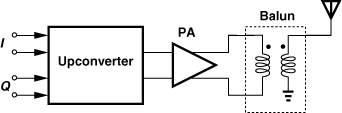
Single-ended PAs, however, suffer from two drawbacks. First, they “waste” half of the transmitter voltage gain because they sense only one output of the upconverter [Fig. 12.8(a)]. This issue can be alleviated by interposing a balun between the upconverter and the PA [Fig. 12.8(b)]. But the balun introduces its own loss, especially if it is integrated on the chip, limiting the voltage gain improvement to a few decibels (rather than 6 dB).
Figure 12.8 Upconverter/PA interface with (a) single-ended or, (b) balun connection.

The second drawback of single-ended PAs stems from the very large transient currents that they pull from the supply to the ground. As shown in Fig. 12.9(a), the supply bond wire inductance, LB1, alters the resonance or impedance transformation properties of the output network if it is comparable with LD. Moreover, LB1 allows some of the output stage signal to travel back to the preceding stage(s) through the VDD line, causing ripple in the frequency response or instability. Similarly, the ground bond wire inductance, LB2, degenerates the output stage and introduces feedback.
Figure 12.9 (a) Feedback in a single-ended PA due to bond wires, (b) less problematic situation in a differential PA.

By contrast, a differential realization greatly eases the above two issues. Illustrated in Fig. 12.9(b), such a topology draws much smaller transient currents from VDD and ground lines, exhibiting less sensitivity to LB1 and LB2 and creating less feedback. The degeneration issue quantified in Example 12.4 is also relaxed considerably.
While the use of a differential PA ameliorates both the voltage gain and package parasitic issues, the PA must still drive a single-ended antenna in most cases. Thus, a balun must now be inserted between the PA and the antenna (Fig. 12.10).
Figure 12.10 Use of a balun between the PA and antenna.
Another useful property of differential PAs is their lower coupling to the LO and hence reduced LO pulling (Chapter 4). If propagating symmetrically toward the LO, the differential waveforms generated by each stage of the PA tend to cancel. Of course, if the PA incorporates symmetric inductors, then the problem of coupling remains (Chapter 7).
The trade-offs governing the choice of single-ended and differential PAs has led to two schools of thought: some TX designs are based on fully-differential circuits with an on-chip or off-chip balun preceding the output matching network, while others opt for a single-ended PA—with or without a balun following the upconverter.
12.2 Classification of Power Amplifiers
Power amplifiers have been traditionally categorized under many classes: A, B, C, D, E, F, etc. An attribute of classical PAs is that both the input and the output waveforms are considered sinusoidal. As we will see in Section 12.3, if this assumption is avoided, a higher performance can be achieved.
In this section, we describe classes A, B, and C, emphasizing their merits and drawbacks with respect to integrated implementation.
12.2.1 Class A Power Amplifiers
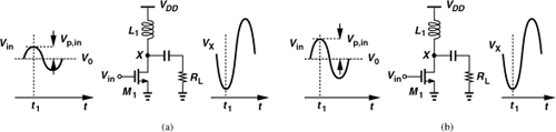
Class A amplifiers are defined as circuits in which the transistor(s) remain on and operate linearly across the full input and output range. Shown in Fig. 12.11 is an example. We note that the transistor bias current is chosen higher than the peak signal current, Ip, to ensure that the device does not turn off at any point during the signal excursion.

The reader may wonder how we define “linear operation” here. After all, ensuring that the transistor is always on does not necessarily imply that the PA is sufficiently linear: if in Fig. 12.11, I1 = 5I2, the transistor transconductance varies considerably from t1 to t2 while the definition of class A seems to hold. This is where the definition of class A becomes vague. Nonetheless, we can still assert that if linearity is required, then class A operation is necessary.
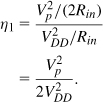
Let us now compute the maximum drain (collector) efficiency of class A amplifiers. To reach maximum efficiency, we allow VX in Fig. 12.11 to reach 2VDD and nearly zero. Thus, the power delivered to the matching network is approximately equal to ![]() , which is also delivered to RL if the matching network is lossless. Also, recall from Example 12.1 that the inductive load carries a constant current of VDD/Rin from the supply voltage. Thus,
, which is also delivered to RL if the matching network is lossless. Also, recall from Example 12.1 that the inductive load carries a constant current of VDD/Rin from the supply voltage. Thus,
The other 50% of the supply power is dissipated by M1 itself.
It is important to recognize the assumptions leading to an efficiency of 50% in class A stages: (1) the drain (collector) peak-to-peak voltage swing is equal to twice the supply voltage, i.e., the transistor can withstand a drain-source (or collector-emitter) voltage of 2VDD with no reliability or breakdown issues;3 (2) the transistor barely turns off, i.e., the nonlinearity resulting from the very large change in the transconductance of the device is tolerable; (3) the matching network interposed between the output transistor and the antenna is lossless.
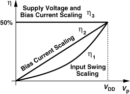
The above example indicates that the minimum drain voltage may not be negligible with respect to VDD, yielding an output swing less than 2VDD. We must therefore compute the efficiency for lower output signal levels. The result also proves useful in transmitters with a variable output power. For example, we note from Chapter 4 that CDMA networks require that the mobile continually adjust its transmitted power so that the base station receives an approximately constant level.
Suppose the PA in Fig. 12.11 must deliver a peak voltage swing of Vp to Rin, i.e., a power of ![]() to the antenna if the matching network is lossless. We consider three cases: (1) the supply voltage and bias current remain at the levels necessary for full output power
to the antenna if the matching network is lossless. We consider three cases: (1) the supply voltage and bias current remain at the levels necessary for full output power ![]() and only the input signal swing is reduced; (2) the supply voltage remains unchanged but the bias current is reduced in proportion to the output voltage swing; (3) both the supply voltage and the bias current are reduced in proportion to the output voltage swing.
and only the input signal swing is reduced; (2) the supply voltage remains unchanged but the bias current is reduced in proportion to the output voltage swing; (3) both the supply voltage and the bias current are reduced in proportion to the output voltage swing.
In the first case, the bias current is equal to VDD/Rin hence and a power of ![]() is drawn from the battery. Consequently,
is drawn from the battery. Consequently,
The efficiency thus falls sharply as the input and output voltage swings decrease.
In the second case, the bias current is reduced to that necessary for a peak swing of Vp, i.e., Vp/Rin. It follows that

Here, the efficiency falls linearly as Vp decreases and VDD remains constant.
In the third case, the supply voltage is also scaled, ideally according to the relation VDD = Vp. Thus,
![]()
While this case is the most desirable, it is difficult to design PA stages with a variable supply voltage. Figure 12.13 summarizes the results.
Figure 12.13 Efficiency as a function of peak output voltage for different scaling scenarios.
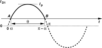
Conduction Angle
It is sometimes helpful to distinguish PA classes by the “conduction angle” of their output transistor(s). The conduction angle is defined as the percentage of the signal period during which the transistor(s) remain on multiplied by 360°. In class A stages, the conduction angle is 360° because the output transistor is always on.
12.2.2 Class B Power Amplifiers
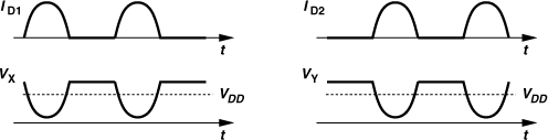
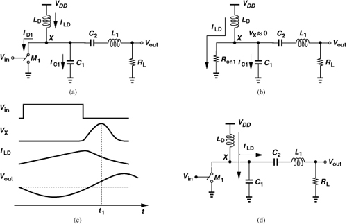
The definition of class B operation has changed over time! The traditional class B PA employs two parallel stages each of which conducts for only 180°, thereby achieving a higher efficiency than the class A counterpart. Figure 12.15 shows an example, where the drain currents of M1 and M2 are combined by transformer T1. We may view the circuit as a quasi-differential stage and a balun driving the single-ended load. But class B operation requires that each transistor turn off for half of the period (i.e., the conduction angle is 180°). The gate bias voltage of the devices is therefore chosen approximately equal to their threshold voltage.

Solution:
Figure 12.16 Output network currents during (a) positive and (b) negative output half cycles.

If the parasitic capacitances are small and the primary and secondary inductances are large, then VX and VY in Fig. 12.15 are also half-wave rectified sinusoids that swing around VDD (Fig. 12.17). In Problem 12.3, we show that the swing above VDD is approximately half that below VDD, an undesirable situation because it results in a low efficiency. For this reason, the secondary (or primary) of the transformer is tuned by a parallel capacitance so as to suppress the harmonics of the half-wave rectified sinusoids at X and Y, allowing equal swings above and below VDD.
Figure 12.17 Current and voltage waveforms in a class B stage.
Let us compute the efficiency of the class B stage shown in Fig. 12.15. Suppose each transistor draws a peak current of Ip from the primary. As explained in Example 12.10, this current flows through half of the primary winding (because the other half carries a zero current). Assuming the turns ratios shown in Fig. 12.18, we recognize that a half-cycle sinusoidal current, ID1 = Ip sin ω0t, 0 < t < π/ω0, produces a similar current in the secondary, but with the peak given by (m/n)Ip. Thus, the total current flowing through RL in each full cycle is equal to IL = (m/n)Ip sin ω0t, producing an output voltage given by
![]()
and delivering an average power of
![]()
Figure 12.18 Class B circuit for efficiency calculation.

We must now determine the average power drawn from VDD. The half-wave rectified current drawn by each transistor has an average of Ip/π (why?). Since two of these current waveforms are drawn from VDD in each period, the average power provided by VDD is equal to
![]()
Dividing Eqs. (12.23) by (12.24) gives the drain (collector) efficiency of class B stages:
![]()
As expected, η is a function of Ip.
In our last step, we calculate the voltage swings at X and Y in the presence of a resonant load in the secondary (or primary). Since the resonance suppresses the higher harmonics of the half-wave rectified cycles, VX and VY resemble sinusoids that are 180° out of phase and have a dc level equal to VDD (Fig. 12.19). That is,
![]()
![]()
Figure 12.19 Class B circuit with resonant secondary network.

The primary of the transformer therefore senses a voltage waveform given by
![]()
which, upon experiencing a ratio of n/(2m), yields the output voltage:
It follows that
![]()
We choose Vp = VDD to maximize the efficiency, obtaining from Eq. (12.25)

In recent RF design literature, class B operation often refers to half of the circuits shown in Figs. 12.15 and 12.18, with the transistor still conducting for only half a cycle. Such a circuit, of course, is quite nonlinear but still has a maximum efficiency of π/4.
As mentioned in Section 12.1.4, the use of an on-chip balun at the PA output lowers the efficiency. For power levels above roughly 100 mW, an off-chip balun may be used if efficiency is critical.
Class AB Power Amplifiers
The term “class AB” is sometimes used to refer to a single-ended PA (e.g., a CS stage) whose conduction angle falls between 180° and 360°, i.e., in which the output transistor turns off for less than half of a period. From another perspective, a class AB PA is less linear than a class A stage and more linear than a class B stage. This is usually accomplished by reducing the input voltage swing and hence backing off from the 1-dB compression point. Nonetheless, the term class AB remains vague.
12.2.3 Class C Power Amplifiers
Our study of class A and B stages indicates that a smaller conduction angle yields a higher efficiency. In class C stages, this angle is reduced further (and the circuit becomes more nonlinear).
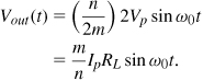
The class A topology of Fig. 12.11 can be modified to operate in class C. Depicted in Fig. 12.20(a), the circuit is biased such that M1 turns on if the peak value of Vin raises VX above VTH. As illustrated in Fig. 12.20(b), VX exceeds VTH for only a fraction of the period, as if M1 were stimulated by a narrow pulse. As a result, the transistor delivers a narrow pulse of current to the output every cycle. In order to avoid large harmonic levels at the antenna, the matching network must provide some filtering. In fact, the input impedance of the matching network is also designed to resonate at the frequency of interest, thereby making the drain voltage a sinusoid.
Figure 12.20 (a) Class C stage and (b) its waveforms.
The distinction between class C and one-transistor class B stages is in the conduction angle, θ. As θ decreases, the transistor is on for a smaller fraction of the period, thus dissipating less power. For the same reason, however, the transistor delivers less power to the load.
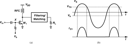
If the drain current of M1 in Fig. 12.20(a) is assumed to be the peak section of a sinusoid and the drain voltage a sinusoid having a peak amplitude of VDD, then the efficiency can be obtained as [7]
![]()
Sketched in Fig. 12.21(a), this relation suggests an efficiency of 100% as θ approaches zero.
Figure 12.21 (a) Efficiency and (b) output power as a function of conduction angle.
The maximum efficiency of 100% is often considered a prominent feature of class C stages. However, another attribute that must also be taken into account is the actual power delivered to the load. It can be proved that [7]
![]()
Applying L’Hopital’s rule, the reader can prove that Pout falls to zero as θ approaches zero. In other words, for a given design, a class C stage provides a high efficiency only if it delivers a fraction of the peak output power (the power corresponding to full class A operation).
How can a class C stage provide an output power comparable to that of a class A design? The small conduction angle dictates that the output transistor be very wide so as to deliver a high current for a short amount of time. In other words, the first harmonic of the drain current must be equal in the two cases.

In modern RF design, class C operation has been replaced by other efficient amplification techniques that do not require such large transistors.
12.3 High-Efficiency Power Amplifiers
The main premise in class A, B, and C amplifiers has been that the output transistor drain (or collector) current and voltage waveforms are sinusoidal (or a section of a sinusoid). If this premise is discarded, higher harmonics can be exploited to improve the performance. Described below are several examples of such techniques. The following topologies rely on specific output passive networks to shape the waveforms, minimizing the time during which the output transistor carries a large current and sustains a large voltage. This approach reduces the power consumed by the transistor and raises the efficiency. We note, however, that the large parasitics of on-chip inductors typically dictate that matching networks be realized externally, making “fully-integrated PAs” a misnomer.
12.3.1 Class A Stage with Harmonic Enhancement
Recall from our study of the class A stage in Fig. 12.11 that, for maximum efficiency, the transistor current swings by a large amount, experiencing nonlinearity. Thus, the current contains a significant second and/or third harmonic. Now suppose the matching network is designed such that its input impedance is low at the fundamental and high at the second harmonic. As illustrated in Fig. 12.23, the sum of the resulting voltage waveforms exhibits narrower pulses than the fundamental, reducing the overlap time between the voltage across and the current flowing in the output transistor. Consequently, the average power consumed by the output transistor decreases and the efficiency increases.
Figure 12.23 Example of second harmonic enhancement.
It is interesting that the above modification need not increase the harmonic content of the signal delivered to the load. The technique simply realizes different termination impedances for different harmonics to make the drain voltage approach a square wave.
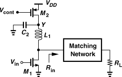
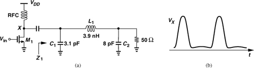
As an example, consider the class A circuit shown in Fig. 12.24(a), where L1, C1 and C2 form a matching network that transforms the 50-Ω load to Z1 = 9 Ω + j0 at f = 850 MHz and Z2 = 330 Ω + j0 at 2f = 1.7 GHz [8]. In this case, the second harmonic is enhanced by a factor of 37. Figure 12.24(b) shows the drain voltage. The circuit delivers a power of 2.9 W to the load with 73% efficiency and a third-order harmonic of −25 dBc [8]. Other considerations for harmonic termination are described in [9]. This enhancement technique can be applied to other PA classes as well.
Figure 12.24 (a) Class A stage with harmonic enhancement, (b) drain waveform.
12.3.2 Class E Stage
Class E stages are nonlinear amplifiers that achieve efficiencies approaching 100% while delivering full power, a remarkable advantage over class C circuits. Before studying class E PAs in detail, we first revisit the simple circuit of Fig. 12.3(a), shown in Fig. 12.25.
Figure 12.25 Output stage with switching transistor.

Suppose the output transistor in this circuit operates as a switch, rather than a voltage-dependent current source, ideally turning on and off abruptly. Called a “switching power amplifier,” such a topology achieves a high efficiency if (1) M1 sustains a small voltage when it carries current, (2) M1 carries a small current when it sustains a finite voltage, and (3) the transition times between the on and off states are minimized [10]. From (1) and (3), we conclude that the on-resistance of the switch must be very small and the voltage applied to the gate of M1 must approximate a rectangular waveform. However, even with these two conditions, (2) may still be violated if M1 turns on when VX is high. Of course, in practice it is difficult to obtain sharp input transitions at high frequencies.
It is important to understand the fundamental difference between the PAs studied in previous sections and the switching stage of Fig. 12.25: in the former, the output matching network is designed with the assumption that the transistor operates as a current source, whereas in the latter, this assumption is not necessary. If the transistor is to remain a current source, then the minimum value of the drain voltage and the maximum value of the gate voltage must be precisely controlled such that the transistor does not enter the triode region. The minimum required drain-source voltage translates to a lower efficiency even if all of the devices and waveforms are ideal. By contrast, in switching amplifiers the drain voltage can approach zero (or even a somewhat negative value).
A serious dilemma in nonlinear PA design is that the gate of the output device must be switched as abruptly as possible so as to maximize the efficiency [Fig. 12.26(a)], but the large output transistor typically necessitates resonance at its gate, inevitably receiving a nearly sinusoidal waveform [Fig. 12.26(b)].
Figure 12.26 (a) Switching stage with sharp input waveform, (b) gradual waveform due to resonance.

Class E amplifiers deal with the finite input and output transition times by proper load design. Shown in Fig. 12.27(a), a class E stage consists of an output transistor, M1, a grounded capacitor, C1, and a series network C2 and L1 [10]. Note that C1 includes the junction capacitance of M1 and the parasitic capacitance of the RFC. The values of C1, C2, L1, and RL are chosen such that VX satisfies three conditions: (1) as the switch turns off VX remains low long enough for the current to drop to zero, i.e., VX and ID1 have nonoverlapping waveforms [Fig. 12.27(b)]; (2) VX reaches zero just before the switch turns on [Fig. 12.27(c)]; and (3) dVX/dt is also near zero when the switch turns on. We examine these conditions to understand the circuit’s properties.
Figure 12.27 (a) Class E stage, (b) condition to ensure minimal overlap between drain current and voltage, (c) condition to ensure low sensitivity to timing errors.

The first condition, guaranteed by C1, resolves the issue of finite fall time at the gate of M1. Without C1, VX would rise as Vin dropped, allowing M1 to dissipate substantial power.
The second condition ensures that the VDS and ID of the switching device do not overlap in the vicinity of the turn-on point, thus minimizing the power loss in the transistor even with finite input and output transition times.
The third condition lowers the sensitivity of the efficiency to violations of the second condition. That is, if device or supply variations introduce some overlap between the voltage and current waveforms, the efficiency degrades only slightly because dVX/dt = 0 means VX does not change significantly near the turn-off point.
The implementation of the second and third conditions is less straightforward. After the switch turns off, the load network operates as a damped second-order system (Fig. 12.28) [10] with initial conditions across C1 and C2 and in L1. The time response depends on the Q of the network and appears as shown in Fig. 12.28 for underdamped, overdamped, and critically-damped conditions. We note that in the last case, VX approaches zero volt with zero slope. Thus, if the switch begins to turn on at this time, the second and third conditions are met.
Figure 12.28 Class E matching network viewed as a damped network.
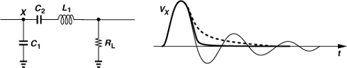
Figure 12.29 (a) Model of class E stage, (b) simplified circuit when transistor is on, (c) voltage and current waveforms, (d) simplified circuit when transistor is off.
Solution:

Class E stages are quite nonlinear and exhibit a trade-off between efficiency and output harmonic content. For low harmonics, the Q of the output network must be higher than that typically required by the second and third conditions. In most standards, the harmonics of the carrier must be sufficiently small because they fall into other communication bands. (Note that a low harmonic content does not necessarily mean that the PA itself is linear; the output transistor may still create spectral regrowth or amplitude compression.)
Another property of class E amplifiers is the large peak voltage that the switch sustains in the off state, approximately 3.56VDD − 2.56VS, where VS is the minimum voltage across the transistor [10]. With VDD = 1 V and VS = 50 mV, the peak exceeds 3 V, raising serious device reliability or breakdown issues.
The design equations of class E stages are beyond the scope of this book. The reader is referred to [10] for details.
12.3.3 Class F Power Amplifiers
The idea of harmonic termination described in Section 12.3.1 can be extended to nonlinear amplifiers as well. If in the generic switching stage of Fig. 12.25 the load network provides a high termination impedance at the second or third harmonics, the voltage waveform across the switch exhibits sharper edges than a sinusoid, thereby reducing the power loss in the transistor. Such a circuit is called a class F stage [11].
Figure 12.30(a) shows an example of the class F topology. The tank consisting of L1 and C1 resonates at twice or three times the input frequency, approximating an open circuit. As depicted in Fig. 12.30(b), VX approaches a rectangular waveform with the addition of the third harmonic.
Figure 12.30 Example of class F stage.
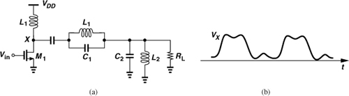
The above example suggests that third-harmonic peaking is viable only if the output transistor experiences “hard” switching, i.e., its output current resembles a rectangular wave. This in turn requires that the gate (or base) voltage be driven by relatively sharp edges.
If the drain current of the transistor is assumed to be a half-wave rectified sinusoid, it can be proved that the peak efficiency of class F amplifiers is equal to 88% for third-harmonic peaking [11].
12.4 Cascode Output Stages
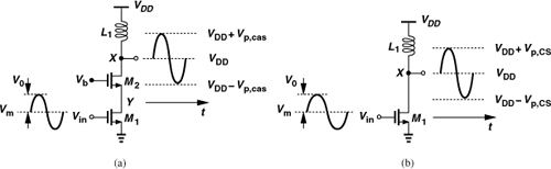
Our study of PA stages in the previous sections reveals that to achieve a high efficiency, the output stage must produce a waveform that swings above VDD. For example, in class A and B efficiency calculations, the drain waveform is assumed to have a peak-to-peak swing of nearly 2VDD. However, if VDD is chosen equal to the nominal supply voltage of the process, the output transistor experiences breakdown or substantial stress. One can choose VDD equal to half of the maximum tolerable voltage of the transistor, but with two penalties: (a) the lower headroom limits the linear voltage range of the circuit, and (b) the proportionally higher output current (for a given output power) leads to a greater loss in the output matching network, reducing the efficiency.
A cascode output stage somewhat relaxes the above constraints. As shown in Fig. 12.31(a), the cascode device “shields” the input transistor as VX rises, keeping the drain-source voltage of M1 less than Vb − VTH2 (why?). Depicted in Fig. 12.31(b) are the typical waveforms: VX swings by about 2VDD and VY by about Vb − VTH (if the minimum drain-source voltages are small).
Figure 12.31 (a) Cascode PA and (b) its waveforms.

In the cascode topology of Fig. 12.31(a), the values of Vb and Vp must be chosen so as to guarantee VDS2 and VDG2 remain below VDD at all times. (The drain-bulk voltage is typically allowed to reach 2VDD or even higher with no reliability concerns.) From Eqs. (12.49) and (12.50), we can write respectively,
![]()
The former is a stronger condition and reduces to
![]()
For example, if Vb = VDD, then Vp ≤ VDD − VTH2; i.e., the peak-to-peak swing at X is limited to 2VDD − 2VTH2. With body effect, VTH2 may reach 0.5 V in 90-nm and 65-nm technologies, yielding a total swing of only 1 Vpp, about the same as that of a noncascoded common-source stage! We therefore observe that the cascode topology offers only a marginal increase in the maximum allowable output swing at low supply voltages.4 Since a cascode topology with a supply voltage of VDD provides an output swing approximately equal to that of a common-source stage with a supply voltage of VDD/2, we expect the former to exhibit an efficiency about half that of the latter, i.e., about 25% in class A operation.
Let us now compare the cascode and CS stages in terms of their linearity. For the stages shown in Fig. 12.32, we seek the maximum output voltage swing that places M1 at the edge of saturation. From Fig. 12.32(a),
![]()
and from Fig. 12.32(b),
![]()
Figure 12.32 (a) Cascode and (b) CS stages for linearity analysis.
It follows that
![]()
Thus, the CS stage remains linear across a wider output voltage range than the cascode circuit does.
The foregoing study suggests that, at low supply voltages, cascode output stages offer only a slight voltage swing advantage over their CS counterparts, but at the cost of efficiency and linearity. Nonetheless, by virtue of their high reverse isolation (a small |S12|), cascode stages experience less feedback, thus proving more stable. As studied in Chapter 5 for low-noise amplifiers, a simple CS stage may suffer from a negative input resistance.
Figure 12.33 (a) Cascade of two CS stages, (b) simplified model of (a), (c) representation of first stage by a resonant impedance.
Solution:
![]()
![]()
![]()
We deal with the transistor-level design of a 6-GHz cascode PA in Chapter 13. The efficiency of the circuit reaches 30% around compression but falls to 5% with enough back-off to satisfy 11a requirements.
12.5 Large-Signal Impedance Matching
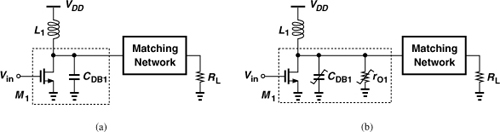
In the development of PAs thus far, we have assumed that the output matching network simply transforms RL to a lower value. This simplistic model of the output network is shown in Fig. 12.34(a), where M1 operates as an ideal current source and L1 resonates with CDB1, allowing the transistor’s RF current to flow into RL. In practice, however, the situation is more complex: the transistor exhibits an output resistance, rO1, and both rO1 and CDB1 vary significantly with VDS1 [Fig. 12.34(b)]. (Recall that for a high efficiency, VDS1 goes from near zero to 2VDD and ID1 from near zero to a large value, creating considerable change in rO1 and CDB1.) Thus, a nonlinear complex output impedance must be matched to a linear load.
Figure 12.34 CS stage with (a) linear drain capacitance and (b) nonlinear drain capacitance and resistance.
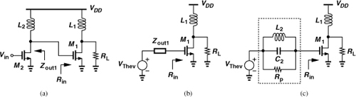
Before dealing with the task of nonlinear impedance matching, let us first consider a simple case where the transistor is modeled as an ideal current source having a linear resistive output impedance [Fig. 12.35(a)]. For a given rO1, how do we choose RL? Let us compute the power delivered by M1 to RL, PRL, and that consumed by the transistor’s output resistance, Pro1. We have
Figure 12.35 Impedance matching with (a) simple transistor model, (b) CDB included, (c) an LC network.
![]()
where Ip denotes the peak amplitude of the transistor’s RF current. Similarly,
![]()
For maximum power transfer, RL is chosen equal to rO1, yielding PRL = Pro1. That is, the transistor consumes half of the power, dropping the efficiency by a factor of two. On the other hand, since
![]()
we recognize that reducing RL minimizes the relative power consumed by the transistor, allowing the efficiency to approach its theoretical maximum (e.g., 50% in class A stages). The key point here is that maximum power transfer does not correspond to maximum efficiency.5 In PA design, therefore, RL is transformed to a value much less than rO1.6
In the next step, suppose, as shown in Fig. 12.35(b), the transistor output capacitance is also included. Note that M1 may be several millimeters wide for an output power level of, say, 100 mW, exhibiting large capacitances. The matching network must now provide a reactive component to cancel the effect of CDB1. Figure 12.35(c) illustrates a simple example where L1 cancels CDB1, and C1 and L2 transform RL to a lower value.
Now consider the general case of a nonlinear complex output impedance. A small-signal approximation of the impedance in the midrange of the output voltage and current can be used to obtain rough values for the matching network components, but modifying these values for maximum large-signal efficiency requires a great deal of trial and error, especially if the package parasitics must be taken into account. In practice, a more systematic approach called the “load-pull measurement” is employed.
Load-Pull Measurement
Let us envision how the matching network interposed between the output transistor and the load must be designed. As conceptually shown in Fig. 12.36(a), a lossless variable passive network (a “tuner”) can present to M1 a complex load impedance, Z1, whose imaginary and real parts are controlled externally. We vary Z1 such that the power delivered to RL remains constant and equal to P1, thus obtaining the contour depicted in Fig. 12.36(b). A low P1 corresponds to a broader range of Re{Z1} and Im{Z1} and hence a wider contour. Next, we seek those values of Z1 that yield a higher output power, P2, arriving at another (perhaps tighter) contour. These “load-pull” measurements can be repeated for increasing power levels, eventually arriving at an optimum impedance, Zopt, for the maximum output power. Note that the power contours also indicate the sensitivity of Pout to errors in the choice of Z1.
Figure 12.36 (a) Load-pull test, (b) contours used in load-pull test, (c) computation of input and output matching impedances.
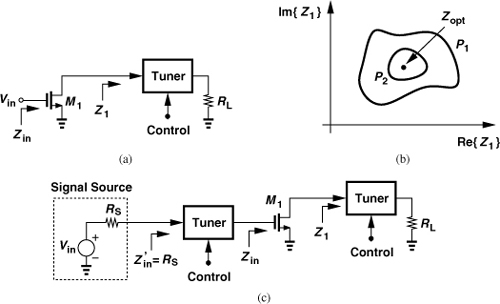
In the above arrangement, the input impedance of the transistor, Zin, has some dependence on Z1 due to the gate-drain capacitance of M1. Thus, the power delivered to the transistor varies with Z1, leading to a variable power gain. This effect can be avoided by inserting another tuner between the signal generator and the gate and adjusting it to obtain conjugate matching at the input for each value of Z1 [Fig. 12.36(c)]. In a multistage PA, however, this adjustment may be unnecessary: after Z1 reaches the optimum, Zin assumes a certain value, and the preceding stage is simply designed to drive Zin.
The load-pull technique has been widely used in PA design, but it requires an automated setup with precise and stable tuners. This method has three drawbacks. First, the measured results for one device size cannot be directly applied to a different size. Second, the contours and impedance levels are measured at a single frequency, failing to predict the behavior (e.g., stability) at other frequencies. Third, since the optimum choice of Z1 in Fig. 12.36(a) does not necessarily provide peaking at higher harmonics, this technique cannot predict the efficiency and output power in the presence of harmonic termination. For these reasons, high-performance PA design using load-pull data still entails some trial and error.
12.6 Basic Linearization Techniques
Recall from Section 12.3 that PAs designed for a high efficiency suffer from considerable nonlinearity. For relatively low output power levels, e.g., less than + 10 dBm (10 mW), we may simply back off from the PA’s 1-dB compression point until the linearity reaches an acceptable value. The efficiency then falls significantly (e.g., to 10% for OFDM with 16QAM), but the absolute power drawn from the supply may still be reasonable (e.g., 100 mW). For higher output power levels, however, a low efficiency translates to a very large power consumption.
A great deal of effort has been expended on linearization techniques that offer a higher overall efficiency than back-off from the compression point does. As we will see, such techniques can be categorized under two groups: those that require some linearity in the PA core, and those that, in principle, can operate with arbitrarily nonlinear stages. We expect the latter to achieve a higher efficiency.
Another point observed in the following study is that linear PAs are rarely realized as negative-feedback amplifiers. This is out of concern for stability, especially if the package parasitics and their variability must be taken into account.
In this section, we present four techniques: feedforward, Cartesian feedback, pre-distortion, and envelope feedback. Two other techniques, namely, polar modulation and outphasing have become popular enough in modern RF design that they merit their own sections and will be studied in Sections 12.7 and 12.8, respectively.
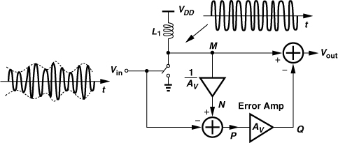
12.6.1 Feedforward
A nonlinear PA generates an output voltage waveform that can be viewed as the sum of a linear replica of the desired signal and an “error” signal. The “feedforward” architecture computes this error and, with proper scaling, subtracts it from the output waveform [12–14]. Shown in Fig. 12.37(a) is a simple example, where the output of the main PA, VM, is scaled by a factor of 1/Av, generating VN. The input is subtracted from VN and the result is scaled by Av and subtracted from VM. If VM = AvVin + VD, where VD represents the distortion content, then
![]()
yielding Vp = VD/Av, VQ = VD, and hence Vout = AvVin.
Figure 12.37 Feedforward linearization.
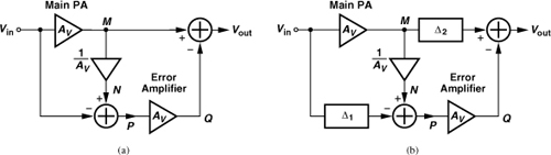
In practice the two amplifiers in Fig. 12.37(a) exhibit substantial phase shift at high frequencies, causing imperfect cancellation of VD. Thus, as shown in Fig. 12.37(b), a delay stage, Δ1, is inserted to compensate for the phase shift of the main PA, and another, Δ2, for the phase shift of the error amplifier. The two paths leading from Vin to the first subtractor are sometimes called the “signal cancellation loop” and the two from M and P to the second subtractor, the “error cancellation loop.”
Avoiding feedback, the feedforward topology is inherently stable if the two constituent amplifiers remain stable, the principal advantage of this architecture. Nonetheless, feed-forward suffers from several shortcomings that have made its use in integrated PA design difficult. First, the analog delay elements introduce loss if they are passive or distortion if they are active, a particularly serious issue for Δ2 as it carries a full-swing signal. Second, the loss of the output subtractor (e.g., a transformer) degrades the efficiency. For example, a loss of 1 dB lowers the efficiency by about 22%.

Third, the linearity improvement depends on the gain and phase matching of the signals sensed by each subtractor. The linearity can be measured by a two-tone test. It can be shown [12] that if the two paths from Vin in Fig. 12.37(b) to the inputs of the first subtractor exhibit a phase mismatch of Δφ and a relative gain mismatch of ΔA/A, then the suppression of the magnitude of the intermodulation products in Vout is given by
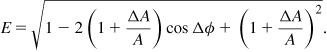
For example, if ΔA/A = 5% and Δφ = 5°, then E = 0.102, i.e., feedforward lowers the IM products by approximately 20 dB. The phase and gain mismatches in the error correction loop further degrade the performance.
Solution:
Figure 12.39 shows the “nested” feedforward architecture [15]. The core PA output is scaled by ![]() , and a delayed replica of the main input is subtracted from it. The error is scaled by
, and a delayed replica of the main input is subtracted from it. The error is scaled by ![]() and summed with the delayed replica of the core PA output.
and summed with the delayed replica of the core PA output.
Figure 12.39 Nested feedforward systems.

While various calibration schemes can be conceived to deal with path mismatches, the loss of the output subtractor (and Δ2) are the principal drawbacks of this architecture.
12.6.2 Cartesian Feedback
As mentioned previously, stability issues make it difficult to apply high-frequency negative feedback around power amplifiers. However, if most of the loop gain necessary for linearization is obtained at low frequencies, the excess phase shift may be kept small and the system stable. In a transmitter, this is possible because the waveform processed by the PA in fact originates from upconverting a baseband signal. Thus, if the PA output is downconverted and compared with the baseband signal, an error term proportional to the nonlinearity of the transmitter chain can be created. Figure 12.41(a) depicts a simple example, where the TX consists of only one upconversion mixer and a PA. The loop attempts to make VPA an accurate replica of Vin, but at a different carrier frequency. Since the total phase shift through the mixers and the PA at high frequencies is significant, the phase, θ, is added to one of the LO signals so as to ensure stability.
Figure 12.41 (a) PA with translational feedback loop, (b) Cartesian feedback.

Note that the approach of Fig. 12.41(a) corrects for the nonlinearity of the entire TX chain, namely, A1, MX1, and the PA. Of course, since MX2 must be sufficiently linear, it is typically preceded by an attenuator.
Most modulation schemes require quadrature upconversion—and hence quadrature downconversion in the above scheme. Figure 12.41(b) shows the resulting topology. In this form, the technique is called “Cartesian feedback” because both I and Q components participate in the loop.
It is instructive to compare the feedforward and Cartesian feedback topologies. The latter avoids the output subtractor and is much less sensitive to path mismatches. However, Cartesian feedback requires some linearity in the PA: if a completely nonlinear PA removes the envelope, no amount of feedback can restore it.
Cartesian feedback faces a severe issue: the choice of the stabilizing LO phase shift [e.g., θ in Fig. 12.41(a)] is not straightforward because the loop phase shift varies with process and temperature. For example, while roaming toward or away from the base station, a cell phone adjusts the PA output level and, inevitably, the chip temperature, making it difficult to select a single value for θ.
12.6.3 Predistortion
If the PA nonlinear characteristics are known, it is possible to “predistort” the input waveform in such a manner that, after experiencing the PA nonlinearity, it resembles the ideal waveform. For example, for a PA static characteristic expressed as y = g(x), predistortion subjects the input to a characteristic given by y = g−1(x) [Fig. 12.42(a)]. Specifically, if g(x) is compressive, predistortion must expand the signal amplitude.
Figure 12.42 (a) Basic predistortion concept, (b) realization in baseband.

Predistortion suffers from three drawbacks. First, the performance degrades if the PA nonlinearity varies with process, temperature, and load impedance while the predistorter does not track these changes. For example, if the PA becomes more compressive, then the predistorter must become more expansive, a difficult task. Second, the PA cannot be arbitrarily nonlinear as no amount of predistortion can correct for an abrupt nonlinearity. Third, variations in the antenna impedance (e.g., how a user holds a cell phone) somewhat affect the PA nonlinearity, but predistortion provides a fixed correction.
Predistortion can also be realized in the digital domain to allow a more accurate cancellation. Illustrated in Fig. 12.42(b), the idea is to alter the baseband signal (e.g., expand its amplitude) such that it returns to its ideal waveform upon experiencing the TX chain nonlinearity. Of course, the above two issues still persist here.

12.6.4 Envelope Feedback
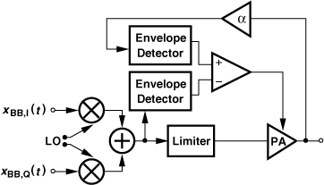
In order to reduce envelope nonlinearity (i.e., AM/AM conversion) of PAs, it is possible to apply negative feedback only to the envelope of the signal. Illustrated in Fig. 12.44, the idea is to attenuate the output by a factor of α, detect the envelope of the result, compare it with the input envelope, and adjust the gain of the signal path accordingly. With a high loop gain, the signals at A and B are nearly identical, thus forcing Vout to track Vin with a gain factor of 1/α.
Figure 12.44 PA with envelope feedback.

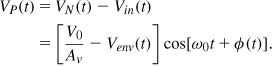
Envelope Detection
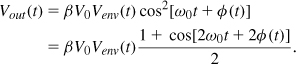
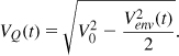
The reader may wonder how an envelope detector can be designed. As shown in Fig. 12.45(a), a mixer can raise the input to the power of two, yielding from Vin(t) = Venv(t) cos[ω0t + φ(t)] the following output
where β denotes the mixer conversion gain. Thus, the low-frequency term at the output is proportional to ![]() . Since the nonlinearity of the envelope detector in the above scheme is not critical, this topology appears a plausible choice.
. Since the nonlinearity of the envelope detector in the above scheme is not critical, this topology appears a plausible choice.
Figure 12.45 (a) Mixer as envelope detector, (b) source follower as envelope detector, (c) limiter and mixer as envelope detector, (d) realization of (c).
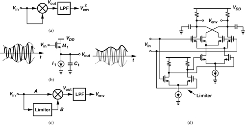
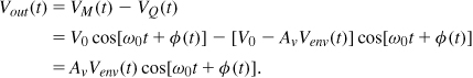
Figure 12.45(b) shows an envelope detector circuit based on “peak detection.” Here, the slew rate given by I1/C1 is chosen much much less than the carrier slew rate so that the output tracks the envelope but not the carrier. As Vin rises above Vout + VTH, Vout tends to track it, but as Vin falls, M1 turns off and Vout remains relatively constant because I1 discharges C1 very slowly. The dimensions of M1 and the values of I1 and C1 must be chosen carefully here: if M1 is not strong enough or C1 is excessively large, then Vout fails to track the envelope itself.
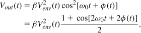
A true envelope detector can be realized if the topology of Fig. 12.45(a) is modified as shown in Fig. 12.45(c). Called a “synchronous AM detector,” the circuit employs a limiter in either of the signal paths, thus removing the envelope variation in that path. Denoting the signal at B by V0 cos[ω0t + φ(t)], we have
The low-pass filter therefore produces the true envelope. Figure 12.45(d) depicts the transistor-level implementation. Here, the limiter transistors must have a small overdrive voltage so that they remove the amplitude variation. In practice, the limiter may require two or more cascaded differential pairs so as to remove envelope variations in one path leading to the mixer.
12.7 Polar Modulation
A linearization originally called “envelope elimination and restoration” (EER) [16] and more recently known as “polar modulation” [17] has become popular in the past ten years. This technique offers two key advantages that allow a high efficiency: (1) it can operate with an arbitrarily nonlinear output stage,7 and (2) it does not require an output combiner (e.g., the subtractor in the feedforward topology).
12.7.1 Basic Idea
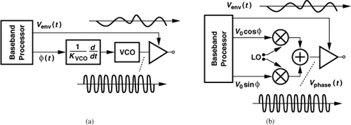
Let us begin with the original EER method. As mentioned in Chapter 3, any band-pass signal can be represented as Vin(t) = Venv(t) cos[ω0t + φ(t)], where Venv(t) and φ(t) denote the envelope and phase components, respectively. We may then postulate that we can decompose Vin(t) into an envelope signal and a phase signal, amplify each separately, and combine the results at the end. Figure 12.46 illustrates the concept. The input signal drives both an envelope detector and a limiting stage, thus generating the envelope, Venv(t), and the phase-modulated component, Vphase(t) = V0 cos[ω0t + φ(t)]. Note that the latter still contains the carrier—rather than only φ(t)—even though it is called the “phase” signal. These signals are subsequently amplified and “combined” in the PA, reproducing the desired waveform. Since the output stage amplifies a constant-envelope signal, Vphase(t), it can be nonlinear and hence efficient. This approach is also called polar modulation because it processes the signal in the form of a magnitude (envelope) component and a phase component.
Figure 12.46 Envelope elimination and restoration.

How should the amplified versions of Venv(t) and Vphase(t) be combined in the output stage? Denoting those versions by A0Venv(t) and A0Vphase(t), respectively, we observe that the desired output assumes the form A0Venv(t) cos[ω0t + φ(t)], i.e., the amplitude of A0Vphase(t) must be modulated by A0Venv(t). It follows that the combining operation must entail multiplication or mixing rather than linear addition.

The combining operation is typically performed by applying the envelope signal to the supply voltage, VDD, of the output stage—with the assumption that the output voltage swing is a function of VDD. To understand this point, let us begin with the simple circuit depicted in Fig. 12.48(a), where S1 is driven by the phase signal. When S1 turns on, Vout jumps to near zero and subsequently rises exponentially toward VDD [Fig. 12.48(b)]. When S1 turns off, the instantaneous change in the inductor current yields an impulse in the output voltage. The output voltage swing is clearly a function of VDD. Note the average areas under the exponential section and the impulse must be equal so that the output average remains equal to VDD.
Figure 12.48 (a) Simple model of output stage, (b) output waveform, (c) stage with capacitances and load resistance, (d) resulting output waveform.

Now consider the more realistic circuit shown in Fig. 12.48(c). In this case, the output waveform somewhat resembles a sinusoid [Fig. 12.48(d)], but its amplitude is still a function of VDD.
The foregoing observations lead to the conceptual combining circuit shown in Fig. 12.49(a), where the envelope signal directly drives the supply node of the PA stage. The large current flowing through this stage requires a buffer in this path, but efficiency considerations demand minimal voltage headroom consumption by the buffer. As an example, the arrangement in Fig. 12.49(b) incorporates a voltage-dependent resistor, M2, to modulate VDD,PA, in proportion to A0Venv(t). For an average current of I0 through L1 and an average voltage drop of V0 across the drain-source resistance of M2, this device dissipates a power of I0V0, lowering the efficiency. Thus, M2 is typically a very wide transistor.
Figure 12.49 (a) Partial realization of EER, (b) output stage with envelope-controlled load, (c) local envelope feedback.

Does the circuit of Fig. 12.49(b) guarantee that VDD,PA tracks A0Venv(t) faithfully? No, it does not: in this “open-loop” control, VDD,PA is a function of various device parameters. This issue becomes more serious if the PA must provide a variable output level because changing the current of the output stage also alters VDD,PA. We may modify the stage to the “closed-loop” control shown in Fig. 12.49(c), where amplifier A1 introduces a high loop gain so that VDD,PA ≈ A0Venv(t). Of course, A1 must accommodate an input common-mode level near VDD.
12.7.2 Polar Modulation Issues
Polar modulation entails a number of issues. First, the mismatch between the delays of the envelope and phase paths corrupts the signal in Fig. 12.46. To formulate this effect, we assume a delay mismatch of ΔT and express the output as
![]()
For a small ΔT, Venv(t − ΔT) can be approximated by the first two terms in its Taylor series:
![]()
It follows that
![]()
The corruption is therefore proportional to the derivative of the envelope signal, leading to substantial spectral regrowth because the spectrum of Venv(t) is equivalently multiplied by ω2. For example, in an EDGE system, a delay mismatch of 40 ns allows only 5 dB of margin between the output spectrum and the required spectral mask [18].
The problem of delay mismatch is a serious one because the two paths in Fig. 12.46 employ different types of circuits operating at vastly different frequencies: the envelope path contains an envelope detector and a low-frequency buffer, whereas the phase path includes a limiter and an output stage.
The second issue relates to the linearity of the envelope detector. Unlike the feedback topology of Fig. 12.44, the polar TX in Fig. 12.46 relies on precise reconstruction of Venv(t) by the envelope detector. As shown in Problem 12.6, this circuit’s nonlinearity produces spectral regrowth.
The third issue concerns the operation of limiters at high frequencies. In general, a nonlinear circuit having a finite bandwidth introduces AM/PM conversion, i.e., exhibits a phase shift that depends on the input amplitude. For example, consider the differential pair shown in Fig. 12.50(a), where the bandwidth is defined by the output pole, ωp = 1/(R1C1). If the input is a small sinusoidal signal at ω0, then the differential output current is also a sinusoid, experiencing a phase shift of
![]()
as it is converted to voltage. For ω0 ![]() ωp,
ωp,
![]()
Figure 12.50 Limiting stage with (a) small and (b) large input swings.

Now, if the circuit senses a large input sinusoid [Fig. 12.50(b)] such that M1 and M2 produce nearly rectangular drain current waveforms, then the delay between the input and output is approximately equal to8
![]()
Expressing this result in radians, we have
![]()
Comparison of Eqs. (12.79) and (12.81) reveals that the phase shift decreases as the input amplitude increases. Thus, the limiter in Fig. 12.46 may corrupt the phase signal by the large excursions in the envelope.
The fourth issue stems from the variation of the output node capacitance (CDB) in Fig. 12.49(c) by the envelope signal. As VDD,PA swings up and down to track A0Venv(t), CDB varies and so does the phase shift from the gate of M1 to its drain, φ0 (Fig. 12.51). That is, the phase signal is corrupted by the envelope signal. This effect can be quantified as follows. We recognize that the variation of CDB alters the resonance frequency, ω1, at the output node. We can therefore express the dependence of φ0 upon the drain voltage as a straight line having a slope of9
![]()
Figure 12.51 AM/PM conversion due to output capacitance nonlinearity.

The first derivative on the right-hand side can readily be found, e.g., from

where VB denotes the junction built-in potential and m is typically around 0.4. The second derivative, dω/dCDB, is obtained from ![]() as
as
Finally, dφ0/dω is computed from the quality factor, Q, of the output network (Chapter 8); that is,
![]()
and hence
![]()
It follows that
![]()
To the first order,
![]()
As mentioned earlier, another issue in polar modulation is the efficiency (and voltage headroom) reduction due to the envelope buffer [M2 in Fig. 12.49(c)]. We will see below that, among the issues outlined above, only the last one defies design techniques and becomes the bottleneck at low supply voltages.
12.7.3 Improved Polar Modulation
The advent of RF IC technology has also improved polar transmitters considerably. In this section, we study a number of techniques that address the issues described in the previous section. The key principle here is to expand the design horizon to include the entire transmitter chain rather than merely the RF power amplifier.
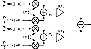
In the conceptual approach depicted in Fig. 12.46, we attempted to decompose the RF signal into envelope and phase components, thus facing limiter’s AM/PM conversion. Let us instead perform this decomposition in the baseband. For an RF waveform Venv(t) cos[ω0t + φ(t)], the quadrature baseband signals are given by
![]()
![]()

In other words, the digital baseband processor can generate Venv(t) and φ(t) either directly or from the I and Q components, obviating the need for decomposition in the RF domain.
While Venv(t) can now be applied to modulate the PA power supply, φ(t) does not easily lend itself to upconversion to radio frequencies. The following example illustrates this point.
Solution:
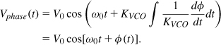
Figure 12.52 Polar modulation using baseband signal separation and (a) a VCO, or (b) a quadrature upconverter.
![]()
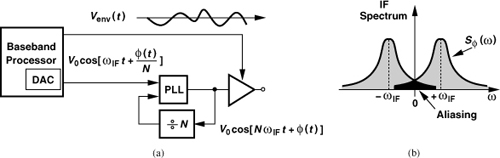
In addition to direct VCO modulation and quadrature upconversion, we studied in Chapter 9 a number of techniques leading to the offset-PLL TX. For example, we contemplated a PLL as a means of upconversion of the phase signal. Figure 12.53(a) depicts an architecture combining that idea with polar modulation. In this case, the phase signal produced by the baseband processor is located at a finite carrier frequency, ωIF, and its phase excursion is scaled down by a factor of N. The PLL thus generates an output given by
![]()
where NωIF is chosen equal to the desired carrier frequency. The value of ωIF must remain between two bounds: (1) it must be low enough to avoid imposing severe speed-power trade-offs on the baseband DAC, and (2) it must be high enough to avoid aliasing [Fig. 12.53(b)].
Figure 12.53 Polar modulation using a PLL in phase path, (b) spectrum of phase signal.
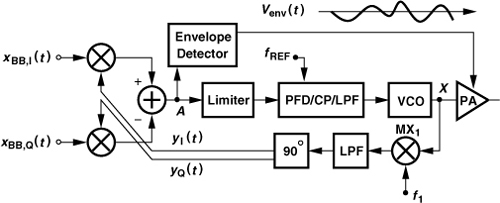
It is possible to combine an offset-PLL TX with polar modulation [19]. Illustrated in Fig. 12.54, the idea is to perform quadrature upconversion to a certain IF, extract the envelope component, and apply it to the PA. The VCO output is downconverted, serving as the LO waveform for the quadrature modulator. Note that the IF signal at node A carries little phase modulation because the PLL feedback forces the phase at A to track that of fREF (an unmodulated reference). With proper choice of the PLL bandwidth, the output noise in the receive band is determined primarily by the VCO design.
Figure 12.54 Polar modulation with phase feedback.
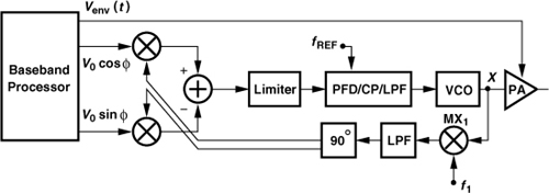
The polar modulation architectures studied above still fail to address two issues, namely, poor definition of the PA output envelope and the corruption due to the PA’s AM/PM conversion (e.g., due to the output capacitance nonlinearity). We must therefore apply feedback to sense and correct these effects. As shown in Fig. 12.49(c), the envelope can be controlled precisely by means of a feedback buffer driving the supply rail of the PA. Alternatively, as in the envelope feedback architecture of Fig. 12.44, the output envelope can be compared with the input envelope. Figure 12.56 depicts the resulting arrangement. The PA output voltage swing is scaled by a factor of α, applied to an envelope detector, and compared with the IF envelope. The feedback loop thus forces a faithful (scaled) replica of the IF envelope at the PA output. The envelope detectors can be realized as shown in Figs. 12.45(c) and (d).
Figure 12.56 Polar modulation with envelope feedback.
In order to correct the PA’s AM/PM conversion, the PA output phase must appear within the PLL, i.e., the PLL feedback path must sense the PA output rather than the VCO output. Illustrated in Fig. 12.57, such an architecture impresses the baseband phase excursions on the PA output by virtue of the high loop gain of the PLL. In other words, if the PA introduces AM/PM conversion, the PLL still guarantees that the phase at X tracks the baseband phase modulation. The two feedback loops present in this architecture can interact and cause instability, requiring careful choice of their bandwidths.
Figure 12.57 Polar modulation with phase and envelope feedback.

Other Issues
The architecture of Fig. 12.57 or its variants [19] resolve some of the polar modulation issues identified in Section 12.7.2. However, several other challenges remain that merit attention.
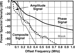
First, the bandwidths of the envelope and phase signal paths must be chosen carefully. The key point here is that each of these components occupies a larger bandwidth than the overall composite modulated signal. As an example, Fig. 12.58 plots the spectra of the individual components and the composite signal along with the spectral mask for an EDGE system [18]. We note that the envelope spectrum exceeds the mask in a few regions and, more importantly, the phase spectrum consumes a much broader bandwidth. If the envelope and phase paths do not provide sufficient bandwidth, then the two components are not combined properly and the final PA output suffers from spectral regrowth, possibly violating the spectral mask. For example, if in an EDGE system the AM and PM path bandwidths are equal to 1 MHz and 3 MHz, respectively, then the output spectrum bears only a 2-dB margin with respect to the mask [18].
Figure 12.58 GSM/EDGE mask margins for a polar modulation system.
While the foregoing considerations call for a large bandwidth in the two paths, we must recall that the PLL specifically serves to reduce the noise in the receive band and, therefore, cannot have a large bandwidth. The trade-off between spectral regrowth and noise in the RX band in turn dictates tight control over the PLL bandwidth. Since the dependence of the charge pump current and KVCO upon process and temperature leads to significant bandwidth variation, some means of bandwidth calibration is often necessary [18].
The second issue relates to the leakage of the PM signal to the output as an additive component. For example, suppose, as shown in Fig. 12.59, the VCO inductor couples a fraction of the PM signal to an inductor (or a pad) at the output of the PA [18].
Figure 12.59 Phase signal leakage path.

Noting the broad bandwidth of the phase signal in Fig. 12.58, we recognize that this leakage produces considerable spectral regrowth if it does not experience proper envelope modulation [18]. This phenomenon can be readily formulated as
![]()
where the second term represents the additive leakage.
The third issue concerns dc offsets in the envelope path [18]. If the envelope produced by the envelope detector has an offset, VOS, then the PA output is given by
![]()
That is, the output contains a PM leakage component equal to A0VOS cos[ω0t + φ(t)], which must be minimized so as to avoid spectral regrowth. For example, in an EDGE system, VOS must remain below 0.2% of the peak of Venv(t) to allow sufficient margin for other errors [18]. Of course, if the output power must be variable, such a condition must hold even for the lowest output level, a difficult task.
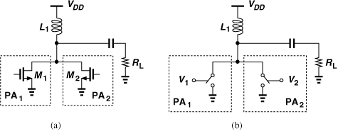
12.8 Outphasing
12.8.1 Basic Idea
It is possible to avoid envelope variations in a PA by decomposing a variable-envelope signal into two constant-envelope waveforms. Called “outphasing” in [20] and “linear amplification with nonlinear components” (LINC) in [21], the idea is that a band-pass signal Vin(t) = Venv(t) cos[ω0t + φ(t)] can be expressed as the sum of two phase-modulated components (Fig. 12.60),
![]()
where
![]()
![]()
and
![]()
Figure 12.60 Basic outphasing.
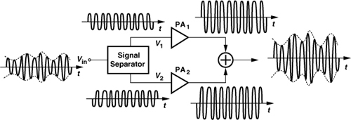
Thus, if V1(t) and V2(t) are generated from Vin(t), amplified by means of nonlinear stages, and subsequently added, the output contains the same envelope and phase information as does Vin(t).
Generation of V1(t) and V2(t) from Vin(t) requires substantial complexity, primarily because their phase must be modulated by θ(t), which itself is a nonlinear function of Venv(t). The use of nonlinear frequency-translating feedback loops has been proposed [21, 22], but loop stability issues limit the feasibility of these techniques. A more practical approach [23] considers V1(t) and V2(t) as
![]()
![]()
where the baseband components are given by
![]()
Since the nonlinear operation required to produce VQ(t) can be performed in the baseband (e.g., using a look-up ROM), this method can simply employ quadrature upconversion to generate V1(t) and V2(t).
The outphasing architecture can operate with completely nonlinear PA stages, an important attribute similar to that of polar modulation. A critical advantage of outphasing is that it does not require supply modulation, saving the efficiency and headroom lost in the envelope buffer necessary in polar modulation. Unfortunately, the summation of the outputs in the outphasing technique entails power loss (as in the feedforward topology).
12.8.2 Outphasing Issues
In addition to the output summation problem, outphasing must deal with a number of other issues. First, the gain and phase mismatches between the two paths in Fig. 12.60 result in spectral regrowth at the output. Representing the two mismatches by ΔV and Δθ, respectively, we have
![]()
![]()
If Δθ ![]() 1 radian, then
1 radian, then
![]()
The last two terms on the right-hand side create spectral growth because they exhibit a much larger bandwidth than the composite signal (the first term).
The second issue concerns the required bandwidth of each path in Fig. 12.60. Since V1(t) and V2(t) experience large phase excursions, φ(t) ± θ(t) (when φ and θ “beat”), these two signals occupy a large bandwidth. Recall from the EDGE spectra in Fig. 12.58 that the bandwidth of a component of the form cos[ω0t + φ(t)] is several times that of the composite signal. This is exacerbated in outphasing by the additional phase, θ(t).

The third issue relates to the interaction between the two PAs through the output summing device. The signal traveling through one PA may affect that through the other, resulting in spectral regrowth and even corruption. To understand this point, let us consider the simple summation shown in Fig. 12.62(a). If M1 and M2 operate as ideal current sources, then one PA’s signal has little effect on the other’s.10 However, it is difficult to achieve a high efficiency while keeping M1 and M2 in saturation.
Figure 12.62 (a) Example of combining circuit, (b) simple model.
Now, suppose M1 and M2 enter the deep triode region and can be modeled as voltage-controlled switches [Fig. 12.62(b)]. In this case, the load seen by one PA is modulated by the other and hence varies with time, distorting the signal.
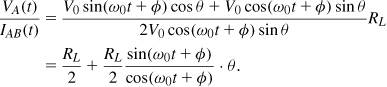
To formulate the interaction between the PAs, we consider the more common arrangement depicted in Fig. 12.63(a), where a transformer sums the outputs11 and drives the load resistance. The output network can be simplified as shown in Fig. 12.63(b). We wish to determine the impedance seen by each PA with respect to ground. To this end, we must compute IAB = (VA − VB)/RL and then Z1 = VA/IAB and Z2 −VB/IAB. If each PA stage is modeled as an ideal voltage buffer with a unity gain, then VA = V1 and VB = V2, yielding
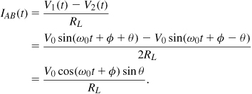
Figure 12.63 (a) Outphasing with a transformer, (b) equivalent circuit.

It follows that
We now assume θ is relatively constant with time, and transform this result to the frequency domain. Since the numerator and denominator of the fraction in the second term are 90° out of phase, they introduce a factor of −j in the equivalent impedance. Thus,
![]()
i.e., the equivalent impedance seen by PA1 consists of a real part equal to RL/2 and an imaginary part equal to (− cot θ)RL/2.12 Similarly,
![]()
The dependence of Z1 and Z2 upon θ reveals that, if the PAs are not ideal voltage buffers, then the signal experiences a time-varying voltage division [Fig. 12.64(a)] and hence distortion. Recognized by Chireix [20], this effect can be alleviated if an additional reactance with opposite polarity is tied to each PA’s output so as to cancel the second term in Eqs. (12.121) or (12.122) [Fig. 12.64(b)]. Since a parallel reactance (admittance) is usually preferred, we first transform Z1 and Z2 to admittances. Inverting the left-hand side of (12.121) and multiplying the numerator and denominator by 1 + j cos θ, we have
![]()
Figure 12.64 (a) Time-varying voltage division in outphasing, (b) Chireix’s cancellation technique.
To cancel the second term,
![]()
and hence
![]()
Similarly,
![]()
To cancel the second term in (12.122),
![]()
and hence
![]()
With perfect cancellation, Z1 = Z2 = RL/(2 sin2 θ). Interestingly, LA and CB resonate at the carrier frequency because
![]()
The foregoing results are based on two assumptions: each PA can be approximated by a voltage source, and θ is relatively constant. The reader may view both suspiciously. After all, a heavily-switching PA stage exhibits an output impedance that swings between a small value (when the transistor is in the deep triode region) and a large value (when the transistor is off). Moreover, the envelope time variation translates to a time-varying θ. In other words, addition of a constant inductance and a constant capacitance to the output nodes provides only a rough compensation.
The reader may wonder if it is possible to construct a three-port power network that provides isolation between two of the ports, thereby avoiding the above interaction. It can be shown that such a network inevitably suffers from loss.
In order to improve the compensation, the inductance and capacitance can track the envelope variation [24]. However, since it is difficult to vary the inductance, we must seek an arrangement that lends itself to only capacitance variation. To this end, let us implement Chireix’s cancellation technique as shown in Fig. 12.65(a). Interestingly, LA and CB shift the resonance frequencies of the two output tanks in opposite directions. We therefore surmise that if only unequal capacitors are tied to A and B and varied in opposite directions, then cancellation may still occur. As depicted in Fig. 12.65(b), we select CA and CB as [24]
![]()
![]()
seeking the proper value of ΔC. The admittances of the tanks are given by
![]()
![]()
where L1 = L2 = L0. Noting that, for a narrowband signal, 1/(jL0ω) and jC0ω cancel, we use Eqs. (12.123) and (12.132) to write the total admittance at A:

Figure 12.65 (a) Outphasing PA using Chireix’s technique, (b) addition of variable capacitances, (c) circuit with discrete capacitor arrays.
The reactive parts cancel if
![]()
Similarly, for node B:

yielding the same ΔC as in (12.136), a fortunate coincidence.
The above development indicates that if ΔC varies in proportion to sin 2θ, then the cancellation is more accurate, leaving a real part in the overall impedance equal to
![]()
Unfortunately, this component also varies with the envelope.13 This issue can be alleviated by adjusting the strength of each PA so as to maintain a relatively constant output power [24]. Figure 12.65(c) shows the result [24], where both the capacitors and the transistors can be tuned in discrete steps. Utilizing bond wires for inductors and an off-chip balun, the PA delivers an output of 13 dBm in the WCDMA mode with a drain efficiency of 27% [24].
12.9 Doherty Power Amplifier
The amplifier stages studied thus far incorporate a single output transistor, inevitably approaching saturation as the transistor enters the triode region (saturation region for bipolar devices). We therefore postulate that if an auxiliary transistor is introduced that provides gain only when the main transistor begins to compress, then the overall gain can remain relatively constant for higher input and output levels. Figure 12.66(a) illustrates this principle: the main amplifier remains linear for input swings up to about V1, and the auxiliary amplifier contributes to the output power as the input exceeds V1. The former operates in class A and the latter in class C.
Figure 12.66 (a) Input/output characteristics of a Doherty PA, (b) hypothetical implementation.

While simple and elegant, the above principle is not straightforward to implement: How exactly should the auxiliary amplifier be tied to the main amplifier? Figure 12.66(b) shows an example where the currents produced by the two branches are simply summed at the output node. However, if the voltage swing at X is large enough to drive M1 into the triode region, then it is likely to drive M2 into the triode region, too.
Recognizing that amplitude-modulated signals reach their peak values only occasionally and hence cause a low average efficiency, Doherty has introduced the above two-path principle and developed the PA topology shown in Fig. 12.67(a) [25]. He has called the main and auxiliary stages the “carrier” and “peaking” amplifiers, respectively. The carrier PA is followed by a transmission line of length equal to λ/4, where λ denotes the carrier wavelength. To match the delay through this line, another λ/4 T-line is inserted in series with the input of the peaking amplifier.
Figure 12.67 (a) Conceptual realization of Doherty PA, (b) equivalent output network.
In order to understand the operation of the Doherty PA, we construct the equivalent circuit shown in Fig. 12.67(b), where I1 and I2 represent the RF currents produced by the carrier and peaking stages, respectively. Our first objective is to determine the impedance Z1. The voltage and current waveforms at a point x along a lossless transmission line are respectively given by
![]()
![]()
where the first term in each expression represents a wave propagating in the positive x direction and the second, a wave propagating in the negative x direction, β = 2π/λ, and Z0 is the line’s characteristic impedance. Since I2 is delayed with respect to I1 by λ/4( = 90°), we write I1 = I0 cos ω0t and I2 = αI0 cos(ω0t−90°) = −αI0 sin ω0t, where α is a proportionality factor signifying the relative “strength” of the peaking stage. Equations (12.140) and (12.141) must now be satisfied at x = 0:
![]()
![]()
and at x = λ/4:
![]()
![]()
Writing a KCL at the output node, we have
![]()
and hence
![]()
![]()
In the last step, we observe that Z1 = −V1/I1, which from Eqs. (12.142) and (12.143) emerges as
![]()
Also, (12.143) yields V+ −V− = −I0Z0 and hence Z1 = −(V+ + V−)/I0. Substituting these values in (12.148) gives
![]()
and
![]()
The key point here is that, as the peaking stage begins to amplify (α rises above zero), the load impedance seen by the main PA falls. This effect counteracts the increase of the main PA drain voltage swings that would be necessary for larger input levels, resulting in a relatively constant drain voltage swing beyond the transition point (Fig. 12.68). One can therefore choose V1 such that the main PA operates in its linear region even for Vin > V1.
Figure 12.68 Current and voltage variation in a Doherty PA.

Several properties of the Doherty PA can be derived [25]. We state the results here: (1) the technique extends the linear range by approximately 6 dB; (2) the efficiency reaches a theoretical maximum of 79% at full output power; (3) this efficiency is obtained if Z0 in Fig. 12.67(a) is chosen equal to 2RL.
The Doherty PA presents its own challenges with respect to IC design. The two transmission lines, especially that at the output, introduce considerable loss, degrading the efficiency. Also, for large swings, the transistor in the peaking stage turns on and off, producing discontinuities in the derivatives of the output current and possibly yielding a high adjacent channel power. In other words, the circuit may prove useful if signal compression must be avoided but not if ACPR must remain small.
12.10 Design Examples
Most power amplifiers employ two (or sometimes three) stages, with matching networks placed at the input, between the stages, and at the output (Fig. 12.69). The “driver” can be viewed as a buffer between the upconverter and the output stage, providing gain and driving the low input impedance of the latter. For example, if a PA must deliver +30 dBm, the two stages in Fig. 12.69 may have a gain of 25 to 30 dB, allowing the upconverter output to be in the range of 0 to + 5 dBm. Depending on the carrier frequency and the power levels, the first matching network, N1, may be omitted, i.e., the driver simply senses the upconverter output voltage.
Figure 12.69 Typical two-stage PA.
The input and output matching networks in Fig. 12.69 serve different purposes: N1 may provide a 50-Ω input impedance, whereas N3 amplifies the voltage swings produced by the output stage (or, equivalently, transforms RL to a lower value). The 50-Ω input impedance is necessary if the PA is designed as a stand-alone circuit that interfaces with the preceding circuit by means of external components. In an integrated TX, on the other hand, the upconverter/PA interface impedance can be chosen quite higher.
The matching network, N2, in Fig. 12.69 is incorporated for practical reasons. Since the design may begin with load-pull measurements on the output transistor, the source impedance that this device must see for maximum efficiency is known and fixed once the design of the output stage is completed. Thus, the driver must drive such an input impedance, often requiring a matching network. In other words, the use of N2 affords a modular design: first the output stage, next the driver, and last the interstage matching, with some iteration at the end. Without N2, the driver and the output stage must be treated as a single circuit and co-designed for optimum performance. While possibly more complex, such a procedure may offer a somewhat higher efficiency because it avoids the loss of N2.
In this section, we study a number of PA designs reported in the literature. As we will see, the efficiency and linearity vary substantially from one design to another. The reader is therefore cautioned that the comparison of the performance of different PAs is not straightforward. In particular, one must ask the following questions:
• What carrier frequency and maximum output power are targeted? The higher these are, the tighter the efficiency-linearity trade-off is.
• How much gain does the PA provide? Designs with lower gains tend to be more linear.
• Does the PA employ off-chip components? Most output matching networks are realized externally to avoid the loss of on-chip devices. For example, some designs incorporate bond wires as part of this network—even though such PAs may be called “fully integrated.”
• Does the IC technology provide thick metallization? For frequencies up to tens of gigahertz, a thick metal lowers the loss of on-chip inductors and transmission lines. (At higher frequencies, skin effect becomes dominant and the benefits of thick metalization diminish.)
• Does the design stress the transistor(s)? Many reported PAs employ a supply voltage equal to the maximum tolerable device voltage, Vmax, but allow above-supply swings, possibly stressing the transistor(s).
• In what type of package is the PA tested? The package parasitics play a critical role in the performance of the PAs.
• Are the efficiency and ACPR measured at the same output power level? Some designs may quote the efficiency at the maximum power but the ACPR at a lower average output.
12.10.1 Cascode PA Examples
Nonlinear PAs can utilize cascode devices to reduce the stress on transistors. Figure 12.70 shows a class E example for the 900-MHz band [26]. Here, M3 and M4 turn on for part of the input swing. The use of a cascode device affords nearly twice the drain voltage swing (compared to a simple common-source stage), allowing the load resistance at the drain to be quadrupled. Consequently, the matching network need only transform 50Ω to about 4.4 Ω for an output power of 1 W, exhibiting smaller losses. For these power levels, the on-resistance of the M1–M2 branch is chosen to be about 1.2 Ω, smaller than other equivalent resistances in the matching network, but requiring a W/L of 15 mm/0.25 μm for each! The large drain capacitance of M2 is absorbed in C1, and the gate capacitance of M1 is tuned by a 2-nH bond wire and an external variable capacitance. Inductors L2 and L3 are also realized by bond wires.
Figure 12.70 Class E PA example.
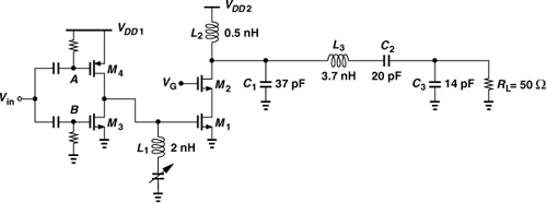
The input stage consisting of M3 and M4 in Fig. 12.70 operates as a class C amplifier because the transistors have a negligible bias current until the swing raises VB above VTH3 or drops VA below VDD − |VTH4|. The PA achieves a power-added efficiency of 41% while delivering 0.9 W with VDD1 = 2.5 V and VDD2 = 1.8 V. The actual design employs two copies of the circuit in quasi-differential form and combines the outputs by means of an off-chip balun [26].
Figure 12.71(a) shows another example of cascode PAs [27]. In order to allow even larger swings at the drain of M2, this topology bootstraps the gate of the cascode device to the output through R1. In other words, since VP and hence VQ rise with Vout, M2 now experiences less stress than if VP were constant. Of course, if VP tracks Vout with unity gain, then M2 operates as a diode-connected device, limiting the minimum value of Vout.14 For this reason, capacitor C1 is added, creating a fraction of the output swing at VP. Figure 12.71(b) plots the circuit’s waveforms, revealing that the maximum drain-source voltages experienced by M1 and M2 can be made approximately equal [27], leading to a large tolerable output swing.
Figure 12.71 (a) Cascode PA with bootstrapping, (b) circuit’s waveforms, (c) addition of diode-connected device.
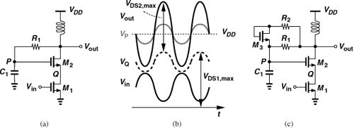
The topology of Fig. 12.71(a) can be further improved by making the bootstrap path somewhat unilateral so that the positive swings are larger than the negative swings. Depicted in Fig. 12.71(c), the modified circuit includes an additional series branch consisting of R2 and a diode-connected device, M3. As Vout rises, M3 turns on, allowing the gate voltage of M2 to follow. On the other hand, as Vout falls, M3 turns off, and only R1 can pull the gate down.

Figure 12.73 shows the overall bootstrapped cascode PA design for the 2.4-GHz band [27]. The dashed box encloses the on-chip circuitry, L1–L3 denote bond wires, and T1–T7 are transmission lines implemented as traces on the printed-circuit board. The output stage utilizes device widths of W3 = 2 mm and W4 = 1.5 mm (with L = 0.18 μm), presenting an input capacitance of roughly 4 pF. In the driver stage, W1 = 600 μm and W2 = 300 μm.
Figure 12.73 Implementation of bootstrapped PA.
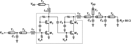
The circuit employs three matching networks: (1) T1, C1, and T2 match the input to 50Ω; (2) T3, L2, and C2 provide interstage matching; and (3) L3, T4–T6, C3, and C4 transform the 50-Ω load to a lower resistance. Transmission line T7 acts as an open circuit at 2.4 GHz.
Operating with a supply of 2.4 V, the PA of Fig. 12.73 delivers a maximum (saturated) output of 24.5 dBm with a gain of 31 dB and a PAE of 49%. The output 1-dB compression is around 21 dBm.
Another example of cascode PA design is conceptually illustrated in Fig. 12.74(a) [28]. Here, a class B stage is added in parallel with a class A amplifier, contributing gain as the latter begins to compress. The operation is similar to that shown in Fig. 12.66(a) for the Doherty PA. The summation of the two outputs faces the same issue illustrated in Fig. 12.66(b), but if the two stages experience compression at the input, then their outputs can be simply summed in the current domain [28]. From this assumption emerges the PA circuit shown in Fig. 12.74(b), where M1−M4 form the main class A stage and M5−M6 the class B path. In this design, (W/L)1,2 = 192/0.8, (W/L)3,4 = 1200/0.34, and (W/L)5,6 = 768/0.18 (all dimensions are in microns). Note that (W/L)5,6 > (W/L)1,2 because the class B devices take over at high output levels. The cascode transistors have a thicker oxide and longer channel so as to allow a higher voltage swing at the output.
Figure 12.74 (a) Parallel class A and B PAs to raise compression point, (b) realization of circuit.

The PA of Fig. 12.74(b) produces a maximum output of 22 dBm with a PAE of 44%. The small-signal gain is 12 dB and the output P1dB is 20.5 dBm.15
12.10.2 Positive-Feedback PAs
Our study of PAs in this chapter has revealed relatively large output transistors and the difficulty in driving them by the preceding stage. Now suppose, as conceptually illustrated in Fig. 12.75(a), the output transistor is decomposed into two, and one device, M2, is driven by an inverted copy of Vout rather than by Vin. The input capacitance of the stage is therefore reduced proportionally. The implementation of the idea becomes straightforward in a differential design [Fig. 12.75(b)]. Since the input devices can now be substantially smaller, they are more easily switched, leading to a higher efficiency.
Figure 12.75 (a) Decomposition of an output device with one section driven by the output, (b) PA driving its own capacitance.

How should the drive capability be partitioned between M1−M3 and M2−M4 in Fig. 12.75(b)? We are tempted to allocate most of the required width to M2−M4 so as to minimize W1 and W3. However, as the design is skewed in this direction, two effects manifest themselves: (1) The capacitance at the output node becomes so large that it may dictate a small resonating inductance (L1 and L2) and hence a low output power. This issue is less problematic in class E stages where the output capacitance can be absorbed in the matching network. (2) As M2 and M4 become wider and carry a proportionally higher current, they form an oscillator with L1 and L2, which are loaded by the equivalent resistance, Rin.
Is it possible to employ an oscillatory PA stage? For a variable-envelope signal, such a circuit would create considerable distortion. However, for a constant-envelope waveform, an oscillatory stage may prove acceptable if its output phase can faithfully track the input phase. In other words, the cross-coupled oscillator must be injection-locked to the input with sufficient bandwidth so that the input phase excursions travel to the output unattenuated. If M1 and M3 in Fig. 12.75(b) are excessively small with respect to M2 and M4, then the input coupling factor may not guarantee locking. Of course, the lock range must be wide enough to cover the entire transmit band. In particular, the lock range can be expressed as
![]()
where Q ≈ L1,2ω/(Rin/2). With a typical Rin of a few ohms, the lock range is usually quite wide.
Figure 12.76 shows a 1.9-GHz class E PA based on injection locking [29]. Both stages incorporate positive feedback, and the inductors are realized by bond wires. In this design, all transistors have a channel length of 0.35 μm, W5−W8 = 980 μm, W1 = W3 = 3600 μm, and W2 = W4 = 4800 μm. Also, L1–L4 = 0.37 nH, L5 = L6 = 0.8 nH, and CD = 5.1 pF. A microstrip balun on the PCB converts the differential output to single-ended form.
Figure 12.76 Injection-locked PA example.

Operating with a 2-V supply and producing a maximum drain voltage of 5 V, the circuit of Fig. 12.76 delivers 1 W of power with a PAE of 48%. It is suited to constant-envelope modulation schemes such as GMSK.
An interesting issue here relates to output power control. While in other topologies, reduction of the input level eventually produces an arbitrarily small output (even if the circuit is nonlinear), injection-locked PAs deliver a relatively large output even if the input amplitude falls to zero (if the circuit oscillates). Figure 12.77 depicts an example where Mp controls the bias current of the output stage. However, to ensure negligible efficiency degradation at the maximum output level, the on-resistance of this device with Vcont ≈ 0 must be very small, requiring a very wide transistor.
Figure 12.77 Injection-locked PA with output power control.
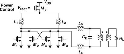
12.10.3 PAs with Power Combining
We have observed in this chapter that transistor stress issues limit the supply voltage and hence output swing of PAs, dictating a matching network with a large impedance transformation ratio. We may alternatively ask, is it possible to directly add the output voltages of several stages so as to generate a large output power.
Let us return to the notion of transformer-based matching [Fig. 12.78(a)]. The on-chip realization of 1-to-n transformers poses many difficulties, especially if the primary and/or secondary must carry large currents. For example, both the series resistance and the inductance of the primary must be kept very small if power levels of greater than hundreds of milliwatts are to be delivered. Also, as explained in Chapter 7, stacked transformers contain various parasitics, and multi-turn planar transformers can hardly achieve a turns ratio of greater than 2. In other words, it is desirable to employ only 1-to-1 transformers.
Figure 12.78 (a) Output stage model using a 1-to-n transformer, (b) circuit using two 1-to-1 transformers to combine the outputs, (c) simple 1-to-1 transformer.

With these issues in mind, we pursue transformer-based matching but using the approach shown in Fig. 12.78(b). Here, the primaries of two 1-to-1 transformers are placed in parallel while their secondaries are tied in series [30]. We expect that the circuit amplifies the voltage swing by a factor of 2 because V1 = V2 = Vin. As exemplified by Fig. 12.78(c), 1-to-1 transformers more easily lend themselves to integration.

How is an actual output stage connected to the double-transformer topology of Fig. 12.78(b)? We can envision the simple arrangement depicted in Fig. 12.79(a), but the long, high-current-carrying interconnects between the amplifier and the two primaries introduce loss and additional inductance. Alternatively, we can “slice” the amplifier into two equal sections and place each in the close vicinity of its respective primary [Fig. 12.79(b)]. In this case, the amplifier input lines may be long, a less serious issue because they carry smaller currents.
Figure 12.79 (a) A single PA or (b) two PAs driving two transformers.
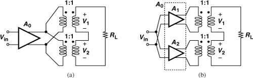
The concept illustrated in Fig. 12.79(b) can be extended to a multitude of 1-to-1 transformers so as to obtain a greater RL/Rin ratio. Figure 12.80 shows a 2.4-GHz class E example employing four differential branches [30]. Each inductor is realized as an on-chip straight, wide metal line to handle large currents with a small resistance. For class E operation, a capacitor must be placed between the drains of each two input (differential) transistors, but the physical distance between N1 and N2, etc., inevitably adds inductance in series with the capacitor. Since the odd-numbered nodes in Fig. 12.80 have the same potential, and so do the even-numbered nodes, the capacitor is tied between, for example, N2 and N3 rather than between N1 and N2.
Figure 12.80 Power combining technique in [30].
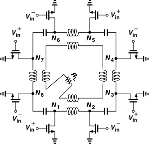
Designed for a 2-W output level [30], the circuit of Fig. 12.80 incorporates wide input transistors. To create input matching, inductors are inserted between ![]() and
and ![]() of adjacent branches. The differential inputs are first routed to the center of the secondary and then distributed to all four amplifiers, thus minimizing phase and amplitude mismatches. One factor limiting the efficiency of transformer-based PAs is the primary/secondary coupling factor, typically no higher than 0.6 for planar structures [30].
of adjacent branches. The differential inputs are first routed to the center of the secondary and then distributed to all four amplifiers, thus minimizing phase and amplitude mismatches. One factor limiting the efficiency of transformer-based PAs is the primary/secondary coupling factor, typically no higher than 0.6 for planar structures [30].
The design in Fig. 12.80 is realized in 0.35-μm technology with a 3-μm thick top metal layer, producing an output of 1.9 W (32.8 dBm) with a PAE of 41%. The PA provides a small-signal gain of 16 dB and runs from a 2-V supply. The output P1dB is around 27 dBm.
The multiple amplifiers driving the 1-to-1 transformers in the foregoing topologies can also be turned off individually, thus allowing output power control [31]. As illustrated in Fig. 12.81, if only M of the N amplifiers are on, then the output voltage swing drops by a factor of N/M. The notable benefit of this approach is that, as the output power is scaled down, it provides a higher efficiency than conventional PAs [31]. [The primary of the off stage(s) must be shorted by a switch.]
Figure 12.81 Power combining with switchable stages.
It is also possible to place the secondaries of the transformers in parallel so as to add their output currents [32].
12.10.4 Polar Modulation PAs
As explained in Section 12.7, a critical issue in polar modulation is the design of the supply modulation circuit for minimum degradation of efficiency and headroom. Figure 12.82 shows an example of an envelope path [33]. Here, a “delta modulator” (DM) generates a replica of Venv at the VDD node of the PA output stage. The DM loop consists of a comparator, a buffer, and a low-pass filter.17 Owing to the high gain of the comparator, the loop ensures that the average output tracks the input even though the comparator produces only a binary waveform.
Figure 12.82 Polar modulation PA using a delta modulator for envelope path.
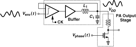
In the circuit of Fig. 12.82, the output stage’s average current flows through the LPF and the buffer. To minimize loss of efficiency and headroom, the LPF utilizes an (off-chip) inductor rather than a resistor, and the buffer must employ very wide transistors. Moreover, the DM loop bandwidth must accommodate the envelope signal spectrum and introduce a delay that can be matched by the phase path.
Figure 12.83 shows an example of a polar modulation transmitter [19]. In contrast to the topologies studied in Section 12.7, this architecture merges the envelope and phase loops: the highly-linear cascade of MX1 and VGA1 downconverts and reproduces both components at an IF, and the decomposition occurs at this IF. The output power is controlled by means of VGA1 and VGA2, e.g., as their gain increases, so does the output level such that the envelope at B remains equal to that at A. This also guarantees that the swing delivered to the feedback limiter is constant and it can be optimized for minimum AM/PM conversion. This transmitter consists of several modules realized in BiCMOS and GaAs technologies. The system delivers an output of +29 dBm in the EDGE mode at 900 MHz [19].
Figure 12.83 Polar modulation PA with envelope and phase feedback.
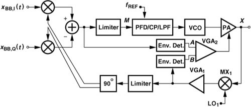
Depicted in Fig. 12.84(a) is another polar transmitter [18]. Here, the quadrature upconverter operates independently, generating an IF waveform having both envelope and phase components. The two signals are then extracted, with the former controlling the output stage and the latter driving an offset PLL.
Figure 12.84 (a) Polar modulation with envelope and phase signals separated at IF, (b) realization of output combining circuit.
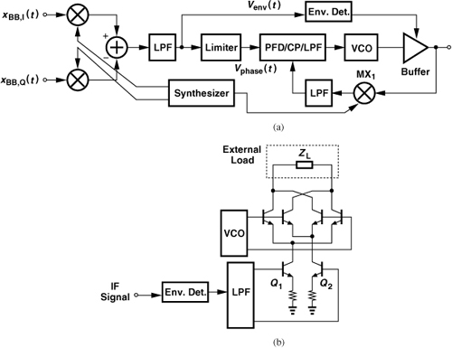
Figure 12.84(b) shows the details of the TX front end. It consists of an envelope detector, a low-pass filter, and a double-balanced mixer driven by the VCO. Designed to deliver a power of +1 dBm, the mixer multiplies the envelope by the phase signal produced by the VCO, thus generating the composite waveform at the output [18]. As mentioned in Section 12.7, the dc offset in the envelope path leads to leakage of the phase component; this TX employs offset cancellation in the envelope path to suppress this effect.
The reader may wonder why the polar transmitters studied above do not employ a mixer of this type to combine the envelope and phase signals. Figure 12.84(b) suggests that the mixer requires a large voltage headroom, consuming substantial power. This technique is thus suited to low or moderate output levels.
12.10.5 Outphasing PA Example
Recall that outphasing transmitters incorporate two identical nonlinear PAs and sum their outputs to obtain the composite signal. Figure 12.85 shows the circuit realization of one PA for the 5.8-GHz band [34, 35]. An on-chip transformer serves as an input balun, applying differential phases to the driver stage. Inductors L1 and L2 and capacitors C1 and C2 provide interstage matching. The output stage operates in the class E mode, with L3–L5 and C3 and C4 shaping the nonoverlapping voltage and current waveforms. Note that the design assumes a load resistance of 12 Ω, a value provided by the power combiner described below.
Figure 12.85 PA used in an outphasing system.

Solution:
Since 15.5 dBm corresponds to 35.5 mW, the peak-to-peak differential voltage swing across RL is equal to ![]() . Thus, the class-E output network in fact reduces the voltage swing by a factor of 3.8 in this case.18 From a device stress point of view, this is undesirable.
. Thus, the class-E output network in fact reduces the voltage swing by a factor of 3.8 in this case.18 From a device stress point of view, this is undesirable.
In order to sum the outputs of the PAs, the outphasing TX employs a “Wilkinson combiner” rather than a transformer. Recall from Section 12.3.2 that a transformer ideally exhibits no loss but it allows interaction between the two PAs. By contrast, a Wilkinson combiner ideally provides isolation between the two input ports but suffers from loss. Shown in Fig. 12.86(a), the combiner consists of two quarter-wavelength transmission lines and a resistor, RT.
Figure 12.86 (a) Wilkinson power combiner, (b) equivalent circuit with differential inputs, (c) equivalent circuit with a common-mode input, (d) input CM impedance.
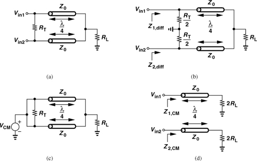
The Wilkinson divider is commonly analyzed in terms of “odd” (differential) and “even” (common-mode) inputs. For differential inputs in Fig. 12.86(a), the output summing junction and the midpoint of RT are at ac ground [Fig. 12.86(b)]. The λ/4 lines transform the short circuit to an open circuit, yielding
![]()
That is, the differential component of Vin1 and Vin2 causes dissipation in RT but not in RL. For a common-mode input, all the points in the circuit rise and fall in unison [Fig. 12.86(c)]. Thus, RL can be replaced with two parallel resistors of value 2RL, and RT with an open circuit [Fig. 12.86(d)]. In this case, the impedance seen by each voltage source is given by
![]()
We recognize that the common-mode component of Vin1 and Vin2 causes dissipation in RL but not in RT.
The result expressed by Eq. (12.162) reveals that the Wilkinson combiner can also transform the load impedance to a desired value if Z0 is chosen properly. The outphasing system in [34, 35] transforms RL = 50Ω to Zin = 12 Ω using Z0 = 35 Ω. The combining of the two differential PA outputs requires four transmission lines, each having a length of 2.8 mm. The on-chip lines are wrapped around the PA circuitry and realized as shown in Fig. 12.87.
Figure 12.87 On-chip Wilkinson combiner used at the output of outphasing system.
Designed in 0.18-μm technology, the outphasing PA of Fig. 12.85 incorporates thick-oxide transistors to sustain a peak drain voltage of 3.5 V. The overall circuit generates an output of 18.5 dBm with an efficiency of 47% while amplifying a 64-QAM OFDM signal.
References
[1] S. Cripps, RF Power Amplifiers for Wireless Communications, Norwood, MA: Artech House, 1999.
[2] A. Grebebbikov, RF and Microwave Power Amplifier Design, Boston: McGraw-Hill, 2005.
[3] A. Johnson, “Physical Limitations on Frequency and Power Parameters of Transistors,” RCA Review, vol. 26, pp. 163–177, 1965.
[4] A. A. Saleh, “Frequency-Independent and Frequency-Dependent Nonlinear Models of TWT Amplifiers,” IEEE Tran. Comm., vol. COM-29, pp. 1715–1720, Nov. 1981.
[5] C. Rapp, “Effects of HPA-Nonlinearity on a 4-DPSK/OFDM-Signal for a Digital Sound Broadband System,” Rec. Conf. ECSC, pp. 179–184, Oct. 1991.
[6] J. C. Pedro and S. A. Maas, “A Comparative Overview of Microwave and Wireless Power-Amplifier Behavioral Modeling Approaches,” IEEE Tran. MTT, vol. 53, pp. 1150–1163, April 2005.
[7] H. L. Kraus, C. W. Bostian, and F. H. Raab, Solid State Radio Engineering, New York: Wiley, 1980.
[8] S. C. Cripps, “High-Efficiency Power Amplifier Design,” presented in Short Course: RF ICs for Wireless Communication, Portland, June 1996.
[9] J. Staudinger, “Multiharmonic Load Termination Effects on GaAs MESFET Power Amplifiers,” Microwave J. pp. 60–77, April 1996.
[10] N. O. Sokal and A. D. Sokal, “Class E - A New Class of High-Efficiency Tuned Single-Ended Switching Power Amplifiers,” IEEE J. of Solid-State Circuits, vol. 10, pp. 168–176, June 1975.
[11] F. H. Raab, “An Introduction to Class F Power Amplifiers,” RF Design, pp. 79–84, May 1996.
[12] H. Seidel, “A Microwave Feedforward Experiment,” Bell System Technical J., vol. 50, pp. 2879–2916, Nov. 1971.
[13] E. E. Eid, F. M. Ghannouchi, and F. Beauregard, “Optimal Feedforward Linearization System Design,” Microwave J., pp. 78–86, Nov. 1995.
[14] D. P. Myer, “A Multicarrier Feedforward Amplifier Design,” Microwave J., pp. 78–88, Oct. 1994.
[15] R. E. Myer, “Nested Feedforward Distortion Reduction System,” US Patent 6127889, Oct., 2000.
[16] L. R. Kahn, “Single-Sideband Transmission by Envelope Elimination and Restoration,” Proc. IRE, vol. 40, pp. 803–806, July 1952.
[17] W. B. Sander, S. V. Schell, and B. L. Sander, “Polar Modulator for Multi-Mode Cell Phones,” Proc. CICC, pp. 439–445, Sept. 2003.
[18] M. R. Elliott et al., “A polar modulator transmitter for GSM/EDGE,” IEEE J. of Solid-State Circuits, vol. 39, pp. 2190–2199, Dec. 2004.
[19] T. Sowlati et al., “Quad-band GSM/GPRS/EDGE Polar Loop Transmitter,” IEEE J. of Solid-State Circuits, vol. 39, pp. 2179–2189, Dec. 2004.
[20] H. Chireix, “High-Power Outphasing Modulation,” Proc. IRE, pp. 1370–1392, Nov. 1935.
[21] D. C. Cox, “Linear Amplification with Nonlinear Components,” IEEE Tran. Comm., vol. 22, pp. 1942–1945, Dec. 1974.
[22] D. C. Cox and R. P. Leek, “Component Signal Separation and Recombination for Linear Amplification with Nonlinear Components,” IEEE Tran. Comm., vol. 23, pp. 1281–1287, Nov. 1975.
[23] F. J. Casadevall, “The LINC Transmitter,” RF Design, pp. 41–48, Feb. 1990.
[24] S. Moloudi et al., “An Outphasing Power Amplifier for a Software-Defined Radio Transmitter,” ISSCC Dig. Tech. Papers, pp. 568–569, Feb. 2008.
[25] W. H. Doherty, “A New High Efficiency Power Amplifier for Modulated Waves,” Proc. IRE, vol. 24, pp. 1163–1182, Sept. 1936.
[26] C. Yoo and Q. Huang, “A Common-Gate Switched, 0.9 W Class-E Power Amplifier with 41% PAE in 0.25-μm CMOS,” VLSI Circuits Symp. Dig. Tech. Papers, pp. 56–57, June 2000.
[27] T. Sowlati and D. Leenaerts, “2.4 GHz 0.18-μm CMOS Self-Biased Cascode Power Amplifier with 23-dBm Output Power,” IEEE J. of Solid-State Circuits, vol. 38, pp. 1318–1324, Aug. 2003.
[28] Y. Ding and R. Harjani, “A CMOS High-Efficiency +22-dBm Linear Power Amplifier,” Proc. CICC, pp. 557–560, Sept. 2004.
[29] K. Tsai and P. R. Gray, “A 1.9-GHz 1-W CMOS Class E Power Amplifier for Wireless Communications,” IEEE J. Solid-State Circuits, vol. 34, pp. 962–970, 1999.
[30] I. Aoki et al., “Fully-Integrated CMOS Power Amplifier Design Using the Distributed Active Transformer Architecture,” IEEE J. Solid-State Circuits, vol. 37, pp. 371–383, March 2002.
[31] G. Liu et al., “Fully Integrated CMOS Power Amplifier with Efficiency Enhancement at Power Back-Off,” IEEE J. Solid-State Circuits, vol. 43, pp. 600–610, March 2008.
[32] A. Afsahi and L. E. Larson, “An Integrated 33.5 dBm Linear 2.4 GHz Power Amplifier in 65 nm CMOS for WLAN Applications,” Proc. CICC, pp. 611–614, Sept. 2010.
[33] D. K. Su and W. J. McFarland, “An IC for Linearizing RF Power Amplifiers Using Envelope Elimination and Restoration,” IEEE J. Solid-State Circuits, vol. 33, pp. 2252–2259, Dec. 1998.
[34] A. Pham and C. G. Sodini, “A 5.8-GHz 47% Efficiency Linear Outphase Power Amplifier with Fully Integrated Power Combiner,” IEEE RFIC Symp. Dig. Tech. Papers, pp. 160–163, June 2006.
[35] A. Pham, Outphasing Power Amplifiers in OFDM Systems, PhD Dissertation, MIT, Cambridge, MA, 2005.
Problems
12.1. Following the derivations leading to Eq. (12.16), prove that the other 50% of the supply power is dissipated by the transistor itself.
12.2. In Fig. 12.16, plot the current from VDD as a function of time. Does this circuit provide the benefits of differential operation? For example, is the bond wire inductance in series with VDD critical?
12.3. Prove that in Fig. 12.17, the voltage swings above and below VDD are respectively equal to ![]() and
and ![]() , where Ip denotes the peak drain current. (Hint: the average value of VX and VY must be equal to VDD.)
, where Ip denotes the peak drain current. (Hint: the average value of VX and VY must be equal to VDD.)
12.4. From Example 12.11, sketch the scaling factor for the output transistor width as α varies from near zero to π/2.
12.5. Compute the maximum efficiency of the cascode PA shown in Fig. 12.31(a). Assume M1 and M2 nearly turn off but their drain currents can be approximated by sinusoids.
12.6. Assuming a third-order nonlinearity for the envelope detector in Fig. 12.46, prove that the output spectrum of the system exhibits growth in the adjacent channels.
12.7. Repeat the calculations leading to Eq. (12.77) but assuming that the phase signal experiences a delay mismatch of ΔT.
12.8. If transistor M2 in Fig. 12.49(b) has an average current of I0 and an average drain-source voltage of V0, determine the efficiency of the stage. Neglect the on-resistance of M1.
12.9. Derive Eq. (12.115) if θ(t) = sin−1[Venv(t)/V1].
12.10. Does the Doherty amplifier of Fig. 12.67(a) operate properly if the input is driven by an ideal voltage source? Explain your reasoning.
12.11. In the Doherty amplifier of Fig. 12.67(a), the value of α is chosen equal to 0.5. Plot the waveforms at x = 0 and x = λ/4, assuming Z0 = RL.