
27
–––––––––––––––––––––––
Increasing Performance through Optimization on APU
Matthew Doerksen, Parimala Thulasiraman, and Ruppa Thulasiram
27.1 INTRODUCTION
As we move into the exascale era of computing, heterogeneous architectures have become an integral component of high-performance systems (HPSs) and high-performance computing (HPC). Over time, we have transitioned from homogeneous central processing unit (CPU)-centric HPSs such as Jaguar [1] to heterogeneous HPSs such as Roadrunner [2], which uses a modified Cell processor and the graphics processing unit (GPU)-based Tianhe-1A [3]. The use of these HPSs has been vital for research applications but, until recently, has not been a factor in the consumer-level experience. However, with new technologies such as AMD’s accelerated processing unit (APU) architecture, which fuses the CPU and the GPU onto a single chip, consumers now have an affordable HPS at their disposal.
27.2 HETEROGENEOUS ARCHITECTURES
To begin, we will provide a basic overview of the different types of heterogeneous architectures currently available. A short list includes the Cell Broadband Engine (Cell BE) [4], GPUs from AMD [5] and NVIDIA, and lastly, AMD’s Fusion APU [6]. Each of these architectures has its own advantages and disadvantages that, in part, determine how well it will perform in a particular situation or algorithm.
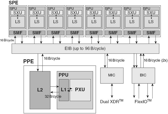
FIGURE 27.1. Cell Broadband Engine processor composed of the power processing element, multiple synergistic processing units and communication enabled via the element interconnect bus [18]. MIC, memory interface controller; SPE, Synergistic Processing Element. BIC, bus interface controller; SXU, synergistic execution unit; PXU, power execution unit; LS, local store.
We now look at the Cell BE, based on the Power Architecture and a collaborative work by Sony, Toshiba, and IBM for HPC for a variety of applications including the most visible, video games. From a high-level perspective, the Cell BE is laid out in a hierarchical structure with the power processing unit at the top and the synergistic processing units (SPU) underneath for computational support.
27.2.1 Cell BE
27.2.1.1 Power Processing Element (PPE) At the top of the hierarchy lies the “master” PowerPC core known as the PPE, which uses a 64-bit Power Architecture with two-way hardware multithreading. The PPE also contains a 32-kB L1 instruction cache and a 32-kB L1 data cache to reduce access times, speeding up computation. Above this is a 512-kB L2 cache to store any data that may be needed during computation. Given that the PPE is the master, it is designed for control-intensive tasks and is able to task switch quickly, making it perfect for running the operating system. Due to this design, however, the PPE is not suited to data-intensive computations, which is why it is supported by up to eight SPUs, which perform the majority of computations. Even so, the PPE is able to execute up to eight single-precision operations per cycle, giving it a theoretical peak performance of 25.6 gigafloating-point operations per second (Gflops) when running at 3.2 GHz (Fig. 27.1).
27.2.1.2 SPUs Each SPU beneath the PPE is a core built for data-intensive applications such as graphics. The SPU uses dual-issue, 128-bit single-instruction multiple-data (SIMD) architecture, which gives it a large amount of computational power for parallel workloads. Each SPU has 128 register files, each of which is 128 bits wide and a 256-kB local data store that holds all instructions and data used by the SPU. Since the SPUs use a SIMD architecture, many features such as out-of-order execution, hardware-managed caches and dynamic branch prediction are absent in an attempt to reduce complexity and die size and to increase performance. These simplifications give the SPU amazing processing power, reaching a single-precision theoretical peak of 25.6 Gflops. Multiplying this value over the eight SPUs, we see that, in total, the Cell BE can provide up to 204.8 Gflops of single-precision performance, greatly outperforming your standard CPU. However, because of the SIMD architecture, SPUs have the disadvantage of large latency times if they do not have data to work on. To reduce this factor of performance, the SPUs connect to the main memory through direct memory access (DMA) commands. DMA allows the SPUs to asynchronously overlap data transfer and computation without going through the PPE in order to hide memory latency. This data transfer occurs over the element interconnect bus (EIB) and is the key to the Cell BE’s performance.
27.2.1.3 EIB The PPE and SPUs communicate with each other and the main memory through the EIB. The EIB is a high-bandwidth, low-latency four-ring structure with two rings running clockwise and two counterclockwise with an internal bandwidth of 96 bytes/cycle. This gives the EIB a maximum 25.6 GB/s in each direction for each port with a sustainable peak throughput of 204.8 GB/s and a 307.2-GB/s maximum throughput between bus units. Additionally, the EIB has support for up to 100 outstanding DMA requests at any given time to ensure the SPUs do not run out of data.
27.2.2 GPUs
After examining the Cell BE, we see it is a very powerful architecture when properly utilized. However, the same implementation that makes it so powerful means that the SPU building blocks are too large to replicate more than a few times. The GPU takes this “slimmed down” approach one step further and uses hundreds of miniature cores (depending on architecture and model) to take advantage of data-parallel work such as graphics. Before we dig any deeper into the GPU architecture and how we will exploit its advantages, we will first examine the GPU’s two main components: the core itself and the off-chip memory. To do so, we turn to AMD’s “Evergreen” architecture, used in their Radeon 5xxx series GPUs [7].
27.2.2.1 GPU Core AMD’s GPUs are composed of many cores that utilize a very long instruction word (VLIW) architecture. We will define each of these miniature cores as stream processors (SPs), which are the smallest block of computational resources. Due to the VLIW design choice, SPs are able to execute up to five (dependent on architecture; from here on we will focus on VLIW5, which is the basis of the Evergreen architecture) operations on the available arithmetic and logic units (ALUs) simultaneously given there are no dependencies. Abstracting these small blocks, we have what are known as SIMD Engines (SEs); these groupings are built out of many SPs (16 in the case of AMD’s current GPU architectures) and are the smallest building block used for each GPU. Before we continue, it should be noted that the number of SEs is often determined by the model of GPU. For example, Figure 27.2 details an AMD Radeon 5870, which contains 20 SEs, while an AMD Radeon 5450 only contains a single SE. Thus, to obtain the shader count for any given GPU for AMD’s Evergreen architecture, we simply multiply the number of SEs by 80 (16 SPs multiplied by 5 because it is a VLIW5 architecture). This vast number of shaders provides the AMD GPU with immense processing power, a single-precision theoretical peak of 2.72 Tflops;even outpacing the Cell by a factor of 10. We also should note that each SE can support 1587 concurrent threads. This allows the Radeon 5870 to support up to 31, 744 concurrent threads, providing a large base for extracting performance out of parallel workloads.
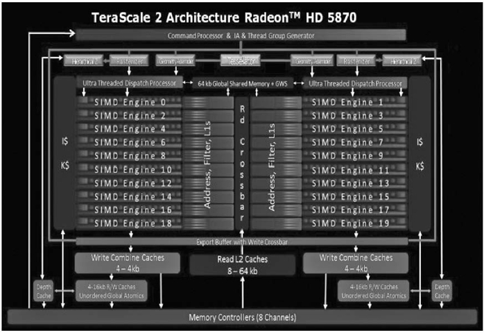
FIGURE 27.2. The TeraScale 2 architecture used in the Radeon 5870 showing the multiple SIMD Engines that comprise the GPU. Upon closer inspection, we can see the 16 SPs that make up a single SIMD Engine [5].
27.2.2.2 VLIW Though the VLIW architecture is very powerful when ALU utilization is high, VLIW architectures are not without flaws. For instance, in cases where very complex operations are used (or instructions are dependent on one another), as few as a single ALU in the SP may be utilized. This leads to a worst-case scenario where theoretical peak performance is limited to one-fifth of the peak performance. It should now be noted that, for simplicity, we assume all instructions take the same amount of time and the four simple ALUs are equal in speed to the single complex ALU (though their supported operations may vary) used in the Evergreen architecture. VLIW also relies heavily on the compiler to properly pack the instructions in order to utilize the ALUs (as opposed to the SIMD approach, which uses hardware to pack instructions dynamically at runtime to improve utilization). It is important to note these drawbacks since the application or algorithm will determine on which type of hardware it will run the best.
27.2.2.3 GPU Off-Chip Memory As important as the GPU core is, the memory subsystem is critical in extracting performance. A GPU core cannot run to the best of its abilities if it is always starved for data (just like the SPUs of the Cell BE); this is where the advanced memory subsystem of AMD’s Evergreen architecture comes into play. The memory subsystem enables high-speed communication between individual shaders and SEs (in general). The first advancement made in the Evergreen architecture was the redesigned memory controller to support error detection code (EDC) for use with higher speed (compared to their previous architectures) Graphics Double Data Rate version 5 (GDDR5) memory. Moving to the shaders, the L2 cache was doubled to 128 kB per memory controller. Additionally, cache bandwidth was also increased from the previous generation to 1 TB/s for L1 texture fetch and 435 GB/s between the L1 and L2 caches. At the highest level, we have a large memory with massive bandwidth for the GPU (for the Radeon 5870, 1–2 GB of GDDR5 memory with 153.6 GB/s of bandwidth). These advances enable the memory system to keep the SEs fed with data in order to maximize the performance of the architecture. However, even with these increases at the GPU level, GPUs are still limited by the additional latency and slow data transfer rate of the PCI Express bus of 16 GB/s in each direction.
27.2.3 APUs
The APU was built in order to combat the memory wall, which is particularly important in systems with discrete GPUs. In a typical system, there is a CPU and a GPU, which must communicate via the PCI Express bus. In an APU-based system, however, the CPU and GPU are on the same chip, meaning there is no need for communication to occur over the PCI Express bus. Each implementation has both advantages and disadvantages, which we will cover as we look at each implementation.
27.2.3.1 Typical Separate CPU/GPU System First, we have Figure 27.3, which shows a traditional system with a separate CPU and GPU [6]. As we already covered, communication between the CPU and GPU must occur over the PCI Express bus. This causes a large performance penalty in both latency and bandwidth, even with the latest PCI Express 3.0 specification. The first advantage of these discrete GPU systems is that multi-GPU support is simplified since we can worry less about differing latencies and bandwidth between dedicated GPUs. Next, these systems are typically built with a larger focus on modularity, enabling performance upgrades much easier than an APU-based system (which would require the replacement of the APU chip, even if we only want a faster CPU or integrated GPU). This modularity comes at its own cost, however, as these types of systems cost more thanan APU system due to the increased number of chips being used (CPU and GPU vs.APU) and the increased complexity required during system design. This, however, is not a major factor in the HPC sector, but for the average consumer, price is one of the key factors in purchasing a system.
27.2.3.2 Fused CPU/GPU System Moving to the APU in Figure 27.4, we have covered that the APU has both the CPU and GPU (in this case, a member of the 5xxx series) on a single chip. This enables the CPU to communicate with the GPU using an on-chip interconnection network rather than the PCI Express bus, reducing latency and increasing bandwidth. While good, this can lead to issues for some types of algorithms.
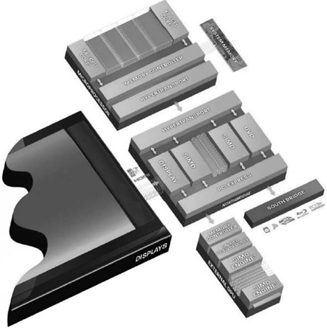
FIGURE 27.3. A typical system with the CPU located at the top of the fi gure, which must communicate with the GPU at the bottom of the fi gure via the PCI Express bus located in the Northbridge [6].
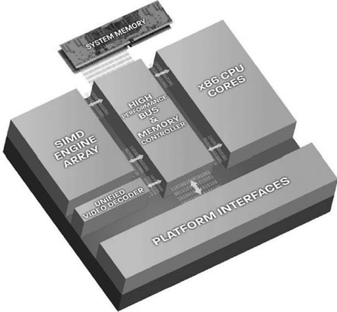
FIGURE 27.4. An APU-based system with a combined CPU and GPU. Note the use of the high-performance on-chip bus that enables communication between the CPU and the GPU at much higher speeds and lower latency than the PCI Express bus [6].
One problem is the potential lack of compute resources as the integrated GPU is a fairly low-end GPU compared to available dedicated GPUs. A second potential problem is the lack of on-chip memory bandwidth. With the APU, the GPU portion only has as much bandwidth as system memory (17 GB/s for a system with dual-channel DDR3 memory running at 1066 MHz), which pales in comparison to the dedicated GPU’s 153.6 GB/s of on-chip bandwidth we noted earlier. From this, it should be simple to see that the APU has corner cases (just like the GPU) where it performs extremely well, such as where data must be moved explicitly back and forth from the CPU to the GPU and vice versa due to algorithmic constraints.
For the large majority of consumers, this is not an issue as few have GPUs above the level of those found in the “standard” APU. It does, however, have the benefit of less expensive systems because fewer hardware components are needed, enabling better performance at lower prices. Looking at things from a programming point of view, an APU system with an additional dedicated GPU is much more difficult to program as we now have to examine the algorithms and determine which ones should execute on which piece of hardware based on the hardware’s characteristics.
27.3 RELATED WORK
27.3.1 The History of Heterogeneous Computing
Heterogeneous computing is not exactly an untouched area; a number of years ago, a few extremely intelligent developers recognized the GPU’s strengths and how it could be used for purposes other than graphics. The problem, however, was that no application programming interface (API) existed to use the GPU for computation. These pioneers began GPU computing by tricking the device into executing code (specified in terms of vertices, vectors, etc.) through the use of the Open Graphics Library (OpenGL). This meant that code was complex and writing it this way was not a viable solution for quick, efficient programs. Eventually, NVIDIA realized the need for a language to abstract the programming issues associated with OpenGL when used for general-purpose computation. We also note that NVIDIA was not the only one with this idea as ATI (which was acquired by AMD in 2006) also worked on two similar projects, namely, Close to Metal and Brook, but has now moved entirely to Open Computing Language (OpenCL). In this section, we will only cover NVIDIA’s solution as it has become the leading GPU compute solution compared to today’s newcomers, OpenCL and DirectCompute.
27.3.2 Compute Unified Device Architecture (CUDA)
Released in 2007, the CUDA framework provided a way to abstract the complication out of using a GPU for general-purpose computation. To do so, NVIDIA started with a C-based language and added specific functionality both in the software development kit (SDK)and driver to handle the difficulties of GPU computing including device setup, memory transfers, and the computation of kernel code. Due to CUDA being the first simple GPU computing language, it gained a large following and became the standard for GPU compute. It has been such a success that both producers and a small number of consumers have taken it to the next level because of the advantages it brings.
To provide a few examples, we look at HPC researchers that have taken NVIDIA GPUs and integrated them into three of the top four supercomputers in the world(as of November 2010). With these supercomputers (and, in general, smaller GPU-based workstations), researchers have built and run CUDA programs in the following areas:
Looking at general results obtained from these applications, researchers were able to speed up computation anywhere from 1.63 times to more than 250 times given the problem type and level of optimization (device specific or general). In all, we see that GPU computing has become an important aspect of the research community because it allows us to run simulations at speeds we never would have thought were possible only a few years ago.
“Regular” consumers, however, have had limited exposure to the advantages of GPU computing. This is due to a few reasons, first being that most consumers will not have a GPU with performance great enough to make GPU computing worthwhile. Second is the price of high-performance GPUs and the associated low market share. For those select few (with high-performance GPUs) that are able to utilize CUDA’s advantages, we see developers integrate GPU computing into programs such as
- Maya’s Shatter plug-in [11]
- Cyberlink’s PowerDVD 10 (and newer) [12]
- enhanced physics calculations in games such as Mafia II [13].
For consumer applications, we will not look at the effect of CUDA in terms of “program X takes Y time units so we can run bigger instances in the same amount of time.” Though this is important for “regular old” computation influencing a user’s experience in terms of wait time, we will instead look at how general-purpose computation using CUDA is able to enhance the user’s experience. To do so, we turn to one of the most visible uses of CUDA in the consumer workspace, gaming. Mafia II, developed by 2K Czech and published by 2K Games, uses CUDA and NVIDIA’s proprietary physics engine, PhysX, for a number of gameplay enhancements including (more) destructible environments, advanced cloth simulations, and more realistic particle-based effects such as smoke and explosions.
Using images taken from Mafia II, we can see the impact that the added GPU computation has on the user experience. When an explosion takes place (see Fig. 27.5), instead of just a few flashy effects, we are able to do much more, such as making the environment destructible or enabling dynamic smoke effects (see Fig. 27.6), allowing many additional bodies in the world with which the player can interact, improving the overall experience. The drawback, however, is that all this extra computation takes time away from the GPU to render the graphical portion of the game. This can be seen in the drop in both current and average frame rates moving from one PhysX setting (off) to another (high), resulting in the game just being playable. Moving back to the user experience, this type of system would only be possessed by a researcher/enthusiast (as the GPU and CPU used in this system cost hundreds of dollars each), pushing this type of user experience out of the regular user’s domain.
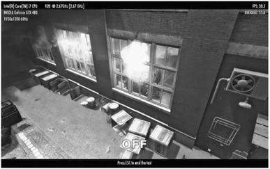
FIGURE 27.5. A screen capture of Mafia II running with PhysX disabled. Note the lack of particles and effects such as smoke and debris [13].
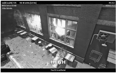
FIGURE 27.6. A second screen capture from Mafi a II but with PhysX enabled. Here we see many more particles such as debris and smoke being added to the user experience [13].
27.4 OPENCL, CUDA OF THE FUTURE
The problem with CUDA is that it will only work with an NVIDIA GPU and, more often than not, requires a powerful GPU as was shown by the framerate change in Mafia II in the previous section. Although NVIDIA recently enabled CUDA to run on the CPU, it still requires running proprietary CUDA code. OpenCL steps in with respect to this and allows a single piece of code to run on any supported platform such as CPUs, GPUs, and most importantly, accelerators (excellent at performing one very specific task) from any supporting vendor including Intel, AMD, and NVIDIA. ARM has also announced its plan to support OpenCL with their next devices, enabling OpenCL to become one of the most pervasive “for consumer use” as well as “for HPC” APIs in the world [14]. In terms of actual developers/companies, Corel (creator of graphic design and video/audio editing software), Blender (a free, open-source 3-D content creation suite), and Bullet (an open-source physics engine) have taken a shine to OpenCL, reinforcing the belief that OpenCL will become the heterogeneous computing API of the future.
27.4.1 OpenCL
Now that we have covered the Cell BE, a discrete GPU system and APU systems as well as the history of GPU computing, we can begin to look at the future of GPU computing, the OpenCL, originally developed by Apple and, in 2008, passed to the Khronos group. From the Khronos website, we have a thorough explanation of OpenCL, after which we will explain its relevance to our applications.
OpenCL is an open, royalty free-standard for cross-platform, parallel programming of modern processors found in personal computer computers, servers and handheld/embedded devices. OpenCL (Open Computing Language) greatly improves speed and responsiveness for a wide spectrum of applications in numerous market categories from gaming and entertainment to scientific and medical software [15].
OpenCL provides a flexible way to program for a heterogeneous architecture usable on almost any combination of operating system and hardware, making it an important starting point for our own applications. We begin with Table 27.1, which provides a quick comparison of OpenCL and CUDA and why we view OpenCL as the computing language of the future.
27.4.2 OpenCL Threading Model
Now that we have a basic understanding of OpenCL, we will look at the threading model OpenCL has in place to help us extract the maximum performance out of our GPUs. In OpenCL, each item or element we wish to compute is known as a work item. From these we have two groupings, one known as the local workgroup, the other being the global workgroup. To simplify the idea, we use Figure 27.7, which shows a square with dimensions of 1024 × 1024. This large square represents our global workgroup composed of 1,048,576 (1024 × 1024) individual work items. From there, we must determine how our work will be split up on an OpenCL device (to create our local workgroups). It is important to note that this value (the maximum local workgroup size) is determined by the OpenCL device itself and is available through documentation or by performing a query of the OpenCL device’s capabilities during runtime. From Figure 27.7 we can see the chosen local workgroup size is 128 × 128 given by 1024 items (width or height) divided into eight groups. This creates a total of 64 local workgroups (that make up the global workgroup) that our OpenCL device will run.
TABLE 27.1. OpenCL versus CUDA, Hardware and Software Support
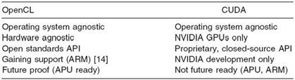
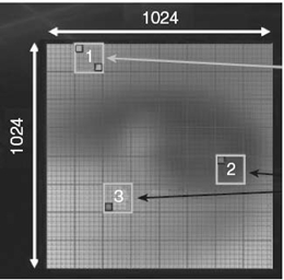
FIGURE 27.7. OpenCL group dimensions are shown: 1, 2, and 3 are local workgroups composed of 128 × 128 elements, while the global workgroup includes 64 workgroups (128 × 128 elements), which total to 1024 × 1024 elements [19].
27.4.2.1 Data Partitioning Workgroup size becomes very important with respect to how we must partition our data for a number of reasons, first, being that all local workgroups are executed in parallel, which means they can be executed in any order. For example, workgroup 3 could be executed before workgroup 1 even though workgroup 1 comes “first” based on numbering. This leads into our next point being that only work items within a local workgroup can be synchronized in order to ensure the correct ordering of operations, such as in group 1. For some tasks, this is not important as all work items may be calculated in parallel if there are no data dependencies. If we are dealing with a situation similar to where group 3 requires some data from group 2, we will have issues. This will mainly consist of the necessity of passing data from one local workgroup to another through global memory (which will be explained momentarily), incurring a large performance penalty in addition to the time required for synchronization.
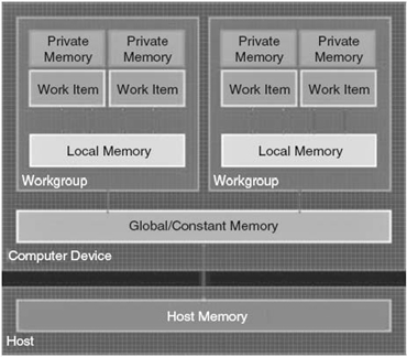
FIGURE 27.8. The OpenCL memory model involves a few different types of memory provided by the GPU. These include the global memory, constant memory, local memory, and private memory. Each of these has a particular purpose, which will be explained in “GPU Memory Types,” Section 27.4.4 [19].
27.4.3 OpenCL Memory Model
OpenCL provides a simple abstraction of device memory, though not to the level given by most modern programming languages. This has the disadvantage of forcing you as the programmer to manage memory, leading to slightly more complex programs. The upside of this manual memory management is that the algorithm can be tuned to take advantage of the incredibly fast memory architecture some devices such as GPUs provide. Before we show the differences between CPU and GPU memories, we will look at the different types of memory OpenCL provides with regard to GPUs as they include more varied and accessible memory than CPUs (Fig. 27.8).
27.4.4 GPU Memory Types
27.4.4.1 Private Memory At the lowest level, we have private memory, which is allocated by the runtime and is given to each thread (recall that each thread is a single work item) in the same manner as memory that is allocated to a CPU [7]. Private memory is not managed by the user other than through simply declaring variables within the OpenCL kernel. Due to this, we will not discuss private memory any further other than its relevance to the other memory types with regard to memory bandwidth.
TABLE 27.2. GPU Memory Types and Bandwidth for AMD Radeon 5870 [20]
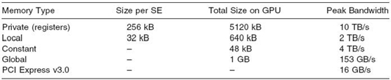
27.4.4.2 Local Memory Next, we have the local memory, which is a block of at least 32 kB that is both read and write accessible to all threads in a local workgroup. We should also make the distinction that local memory is not a single block split over all workgroups, but rather, each local workgroup has its own 32 kB of local memory for its threads to share. This local memory is essentially a user-managed cache to speed access of items that are used within a workgroup. Another feature of local memory that is key to performance is the lack of mandatory memory coalescing. In layman’s terms, without coalesced memory, out-of-order memory requests are performed sequentially instead of in parallel; local memory solves this problem for us. Local memory is an incredibly powerful tool when extracting performance since it is able to provide each SE with more than 100 GB/s of bandwidth, totaling over 2 TB/s for the entire GPU in the case of the AMD Radeon 5870.
27.4.4.3 Constant Memory Constant memory (in the Radeon 5870) provides the second fastest method to access data with registers being the only faster type of storage. To give some hard numbers, we look at Table 27.2 to analyze the memory resources of a Radeon 5870. Note that some of the numbers will need to be changed based on the model of GPU as some hardware may be fused off, reducing the total amount of memory and aggregate bandwidth.
As we can see, registers obviously provide the most bandwidth at 10 TB/s, while constant memory can transfer 4 TB/s and local memory being limited to a “paltry” 2 TB/s. Due to constant memory’s high bandwidth, we should attempt to use constant memory wherever possible. The drawback of constant memory is, obviously, that it is read only and is limited to 48 kB for the entire GPU as opposed to the 640 kB of local memory. The idea we are pushing is that the PCI Express bus should be avoided at all costs due to its increased latency and low bandwidth compared to any on-chip GPU memory. This includes global memory, which operates at a factor of roughly 1/13th the speed of local memory.
27.4.4.4 Global Memory Up next is the global memory on the GPU device. It is a slow type of memory compared to the caches, constant and local memories, but it is accessible from all workgroups. This property enables global synchronization at the cost of increased latency and reduced bandwidth. Global memory also serves as the access point between the host (the CPU) and a compute device (a CPU [which can be the same as the host], GPU, or other accelerator). This means that you as the programmer must explicitly move data from the host to the device (and into local, constant, etc., memory) and back.
TABLE 27.3. CPU Memory Types and Bandwidth for Intel Xeon X5570 [21]
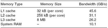
27.4.5 CPU Memory Types
There is a large difference in the memory available to CPUs as opposed to GPUs. CPUs typically have the caches abstracted out of the programming model and thus do not allow the programmer to choose a particular memory type to use. This abstraction causes problems with OpenCL code written for a GPU device when it is run on the CPU as local and global/constant memory are emulated in host/main memory (as the CPU does not have user accessible caches like the GPU). This leads to situations where local memory appears to have no benefit on the CPU but is quite beneficial on the GPU. This is an important difference to note as it goes to show that with OpenCL, no single algorithm can extract maximum performance from an architecture without being properly tuned. Additionally, we provide the following table just to show the difference in memory speed between CPUs and GPUs (see Table 27.3).
27.5 SIMPLE INTRODUCTION TO OPENCL PROGRAMMING
To give you a basic idea of what OpenCL code consists of, we will now look at a very simple, unoptimized algorithm after which we will implement a few optimization techniques to improve performance. Before we begin, if you have not read Section 27.2, “Heterogeneous Architectures,” earlier, please go back and do so to gain a better understanding of the GPU architecture. This will provide the background regarding why the code looks like it does and should enable a basic understanding of how and why the optimization techniques work. You should also read over the OpenCL section once more to become familiar with the terminology used here and to begin to understand, from a high level, the OpenCL model of programming. Lastly, in an effort to abstract the complexity out of the host code, we will simply provide a pseudocode as this is not as important as the kernel code itself.
First, we look at the pseudocode for the host that is required to set up an OpenCL device, set parameters, enqueue a kernel for execution, and retrieve results with respect to a simple program. This program will take three values from an array of size 256 (to eliminate the complexities of scaling the algorithm for beginners), sum them together, and store them in a separate array.
Listing 27.1: OpenCL Host Program
Next, for the sake of readability, please see the Appendix to view the OpenCL kernel codes, which, while very simple, show how an OpenCL program is very similar to a standard C program.
There are a few things to mention when looking at the code, which may be different from a similar code in C. We begin with the function declaration, which has two main points that differ from a function header in C. In OpenCL, every kernel is prefixed with “__kernel” to differentiate it from a standard function (even though OpenCL kernels can be called from the CPU). Next is that we have “__global” prefixed to certain variables in the header. The purpose of this is to show where these variables (or arrays in our case) will be stored on the device. In this example, we have chosen to store the arrays in the large, slow global memory, although local, constant, and texture memories are also options.
Now inside the kernel, we retrieve the thread ID, which is unique to each thread (using the get_global_id() function, as a sidenote, a get_local_id() function also exists) so that it knows which piece of data it should be working on. If we were to implement this same algorithm on a CPU, we would see one major difference: the use of a loop to go through each position of the new array and calculate its value. With OpenCL, we must change our thinking from “single thread executing all elements” to “hundreds or thousands of threads executing simultaneously.” When thinking in these terms, we see that by executing the code on the OpenCL device, we define the outer loop in terms of parameters when setting up the kernel, such as creating a global workgroup of, say, 256 items. This way, we will have 256 threads executing one item in the OpenCL version, while the same sequential CPU code would have a loop so that one thread calculates all 256 items. This concludes the introduction to OpenCL programming section of this chapter, but continue reading to see how we can make some changes to the algorithm to speed it up.
27.5.1 A Few Optimization Techniques
Now that we have a basic algorithm that works correctly, we would like to improve performance. If we were designing an algorithm for the CPU, there would not be much more additional optimization that could be performed because CPU compilers are already very good at making optimizations for a particular device architecture. Since we are using a heterogeneous device, compilers are not yet as advanced as we would like them to be. This forces us to manually perform optimizations that eventually will be done by the compiler to maximize performance for the particular device architecture. In this section, we will cover a few techniques at a high level and explain why we try to use this optimization technique.
27.5.1.1 Local Memory The first optimization we will look at is local memory, which can, depending on the nature of memory access in the algorithm (e.g., random and sequential), speed up the algorithm by a large factor due to the difference in speed, roughly 10 times if the algorithm is limited by memory speed. To begin, we can reuse almost the entire source code from earlier, but we must now add another buffer in the host code for the local memory (not shown). Additionally, because local memory is not directly accessible, we must move data from the host’s memory to global memory to local memory (and back if necessary).
In the source code itself (see Appendix), we now have the additional buffer “loc_input.” We prefix the name with “__local” to show that we would like this array to be created in the device’s local memory as opposed to the device’s global memory. Next, we copy over the data from global memory into local memory. Then, we have a new command, “barrier,” which forces a synchronization step to occur. Synchronization is used to ensure all threads executing the code stop and wait until all other threads have also reached the synchronization point. This is necessary because, if we look at the code, we are reading from locations −1 to +1 of our ID. These values must be loaded into local memory before we execute the code; otherwise, we may retrieve incorrect (or uninitialized) values from local memory. The final change to our source code includes changing the read location from “input” to “loc_input” since we are now using local memory.
27.5.1.2 Vectorization Another technique for improving performance is vectorization. From the earlier section on VLIW architectures, vectorization packs multiple small instructions into a single large instruction that the hardware can execute at one time. The simple example we provide performs two computes and stores per thread, which do not have any dependencies. Under a traditional model, there would be two individual instructions, which would be executed sequentially. Using vectorization, however, we have two instructions, each of which can be executed in parallel, potentially speeding up execution by two times. We will also note that vectorization support by current AMD GPUs is up to 16 items in parallel (though the hardware only supports a maximum of 4).
While vectorization does have the potential to speed up many of our computations, it also does complicate the code. First is that the host code must be changed to work with vectorized OpenCL data types such as the “cl_int2” type used here, rather than the simple “int” type used previously. We must also change the kernel header to note this new data type. This was done by changing the input data type to “int2” from “int.” Finally, we have the calculations themselves as we must now manually determine how to map the work so that we get good device utilization. This can be seen in the kernel code (see the Appendix), which now has three extra calculations (one per “if” statement) in order to be able to execute two elements simultaneously.
27.6 PERFORMANCE AND OPTIMIZATION SUMMARY
If we were to use these algorithms and scale up the input to a large value such as 30,000 elements, we would see that even a simple GPU can provide extraordinary computational power if the algorithm has a large amount of data parallelism. What we have not covered here is that GPU solutions do not do well when data sizes are small. This is to be expected because we are more limited by the time it takes to transfer data back and forth from the GPU than the actual computation does (compared to the CPU). Providing a short summary of the advantages and disadvantages of each algorithm, we begin with the basic kernels that use global and local memory.
Overall, this is a very basic kernel that would work well as the array size increases, particularly since global memory is very large, enabling us to hold the entire array in just one memory location. The downside to this simple algorithm is that global memory is very slow compared to the other types of memory, and thus, we lose out on a large amount of performance. To somewhat alleviate this problem, we brought in the use of local memory, which can be many times faster than global memory. This has its own downsides, though, as local memory is not only small but is also subject to bank conflicts (two or more threads accessing the same memory location), which cause memory requests to be done sequentially, degrading performance. We will also note that bank conflicts may be introduced because of our next technique, as we are storing multiple subelements into a data type.
Next, in an effort to increase device utilization, we introduced vectorization, a method of packing independent instructions so that they may be executed in parallel. Vectorization also has its own problems, namely, it requires (at times) manually coding which work can be done in parallel, and vectorization may cause branching, which, on GPUs can drastically hurt performance as each branch must be executed sequentially. Lastly, vectorization is only beneficial on AMD GPUs due to their VLIW architecture (NVIDIA GPUs support vectorization but, because they use scalar ALUs, vectorized instructions are still executed sequentially). This concludes the optimization section of the chapter where we introduced a few techniques to improve GPU performance, though other techniques such as loop unrolling also exist.
27.7 APPLICATION
Now that we have covered some of the basics of OpenCL programming and a few of the optimization techniques that can be applied, we will look at the 0-1 knapsack problem to show how GPU computing performs. We begin with Figure 27.9 [16], which shows the execution times of the 0-1 knapsack problem for various sizes when run sequentially, in parallel, and on the GPU. As we can see, this naive algorithm does not perform well on the GPU simply because we are forcing synchronization to occur after each iteration. We also are limited to just 256 items for this initial GPU implementation as that is the largest size allowable for a single local workgroup.
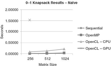
FIGURE 27.9. The execution times from running a naive 0-1 knapsack algorithm on both a CPU and a GPU [16].
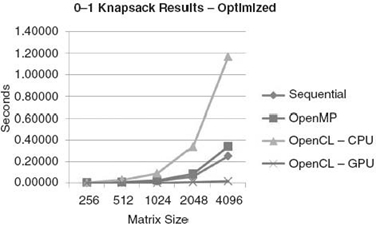
FIGURE 27.10. The execution times from running an optimized 0-1 knapsack algorithm on both a CPU and a GPU [16].
Next, Figure 27.10 shows the execution times for the algorithm optimized to take advantage of local memory and to avoid returning to the CPU for synchronization after every iteration. In this case, the algorithm has also been scaled up so that it supports input sizes greater than 256 items, enabling the parallel nature of the GPU to shine. Here, we see a drastic increase in performance compared to the previous algorithm for the GPU. However, upon closer examination, the OpenCL algorithm running on the CPU has actually become slower. This is due to the optimizations for the GPU, which add synchronization, something the CPU performs very poorly at compared with the GPU.
We now end with Figure 27.11 to show the speedup of the algorithm compared to the sequential algorithm. From the graph, we see that even with a relatively small input size of 512, the GPU is much faster than the CPU with the difference only becoming greater at larger input sizes. However, we should note that this algorithm was not fully optimized to take advantage of all the compute units within the GPU, leaving a large amount of performance untapped. It did, however, use a few of the optimization techniques we talked about in the previous section such as local memory and loop unrolling.
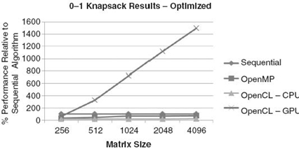
FIGURE 27.11. The speedup of the GPU algorithm compared to the sequential CPU algorithm [16].
27.8 SUMMARY
This has been a very simple introduction to heterogeneous architectures and OpenCL’s programming model and performance. We hope you have enjoyed this intoduction to OpenCL enough to take a serious look at its use for HPC. If you wish to learn more about OpenCL, please visit the Khronos website [15]. If you want to learn more about existing applications using AMD’s Accelerated Parallel Processing SDK with examples using OpenCL, you can visit AMD’s developer web page [17]. We will now spend a little time recapping everything we have learned about OpenCL and HPC. We have learned that there are various architectures, each of which has its own strengths and weaknesses. GPUs are of particular interest to us as they provide a great deal of computational power when used with algorithms that have a large amount of data parallelism. APUs, on the other hand, are somewhat weaker in terms of execution units but have the benefit of increased bandwidth and reduced latency between the CPU and GPU, enabling many more algorithms to be accelerated. We have seen that OpenCL can be used to extract the performance of the GPU in a simple example, and in the future, we will study more advanced OpenCL features to enable APU computing in situations where standard GPU computing is not possible.
Appendix
LISTING A.2: OPENCL KERNEL
LISTING A.3: OPENCL KERNEL OPTIMIZATION 1: LOCAL MEMORY
LISTING A.4: OPENCL KERNEL OPTIMIZATION 2: VECTORIZATION
REFERENCES
[1] No author listed, Top500—Jaguar. Available at http://top500.org/system/10184.
[2] No author listed, Top500—Roadrunner. Available at http://top500.org/system/10377.
[3] No author listed, Top500—TianHe-1A. Available at http://top500.org/system/10587.
[4] J.A. Kahle, M.N. Day, H. Hofstee, C.R. Johns, T.R. Maeurer, and D. Shippy, “Introduction to the Cell multiprocessor,” IBM Journal of Research and Development, 49(4.5): 589–604, 2005.
[5] Advanced Micro Devices, Heterogeneous Computing OpenCLTM and the ATI RadeonTM HD 5870 (“Evergreen”) Architecture. Available at http://developer.amd.com/gpu_assets/ Heterogeneous_Computing_OpenCL_and_the_ATI_Radeon_HD_5870_Architecture _201003.pdf.
[6] N. Brookwood, AMD FusionTM Family of APUs: Enabling a Superior, Immersive PC Experience. March 2010.
[7] B. Gaster, L. Howes, D.R. Kaeli, P. Mistry, and D. Schaa, Heterogeneous Computing with OpenCL. Waltham, MA: Morgan Kaufmann, 2011.
[8] L. Pan, L. Gu, and J. Xu, “Implementation of medical image segmentation in CUDA,” in International Conference on Information Technology and Applications in Biomedicine, 2008. Shenzhen, China, pp. 82–85, May 2008.
[9] L. Nyland and J. Prins, “Fast N-body simulation with CUDA,”Simulation, 3: 677–696, 2007.
[10] D. Komatitsch, D. Michéa, and G. Erlebacher, “Porting a high-order finite-element earthquake modeling application to NVIDIA graphics cards using CUDA,” Journal of Parallel and Distributed Computing, 69(5): 451–460, 2009.
[11] “Maya Shatter .” Available at http://www.nshatter.com/index.html.
[12] Video Editing Software, Multimedia Software and Blu-ray Playback Software by CyberLink. Available at http://www.cyberlink.com/.
[13] Guides: Mafia II Tweak Guide—GeForce. Available at http://www.geforce.com/#/ Optimize/Guides/mafia-2-tweak-guide.
[14] A. Lokhmotov, Mobile and Embedded Computing on MaliTMGPUs. December 2010. Available at http://www.many-core.group.cam.ac.uk/ukgpucc2/talks/Lokhmotov.pdf.
[15] OpenCL—The Open Standard for Parallel Programming of Heterogeneous Systems. Available at http://www.khronos.org/opencl/.
[16] M. Doerksen, S. Solomon, P. Thulasiraman, and R.K. Thulasiram, “Designing APU oriented scientific computing applications in OpenCL,”IEEE 13th International Conference on High Performance Computing and Communications (HPCC), Banff, Canada, pp. 587–592, September 2011.
[17] “AMD APP Developer Showcase,” Available at http://developer.amd.com/sdks/ AMDAPPSDK/samples/showcase/Pages/default.aspx.
[18] M. Gschwind, “Chip multiprocessing and the cell broadband engine,” in Proceedings of the 3rd Conference on Computing frontiers, CF’06, pp. 1–8, ACM, 2006.
[19] B.R. Gaster and L. Howes, OpenCLTM—Parallel Computing for CPUs and GPUs. July 2010. Available at http://developer.amd.com/zones/OpenCLZone/courses/Documents/ AMD_OpenCL_Tutorial_SAAHPC2010.pdf.
[20] Advanced Micro Devices, Ati Stream SDK OpenCL Programming Guide. June 2010. Available at http://developer.amd.com/gpu_assets/ATI_Stream_SDK_OpenCL_Programming_Guide.pdf.
[21] D. Molka, D. Hackenberg, R. Schone, and M.S. Muller, “Memory performance and cache coherency effects on an intel nehalem multiprocessor system,” in 18th International Conference on Parallel Architectures and Compilation Techniques, Raleigh, NC, pp. 261–270, September 2009.