
Electronic analogue switching, Part I: CMOS gates
In the course of the years spent designing mixing consoles, I came to know a great deal about analogue switching. All but the most basic mixers have a PFL system – the acronym meaning Pre-Fade Listen. In other words you can press a button on an input channel and have its contribution alone heard through your monitor speakers without disturbing the flow of signals to the main outputs. This requires the feed to the monitors to be switched, and for many years the only way to do this was a double-pole relay going ‘clunk’ somewhere in the console. It was a great relief to all concerned when the arrival of the 4016 analogue switch meant that this function could be performed electronically. It was cheap, reliable, and acoustically silent, and if the linearity was not perfect it was quite good enough. The chapter on mixing console design ‘Inside Mixers’ in this book gives more details on PFL systems and the like.
But why did discrete FET switching, as described in the second of these chapters, become so popular? It needs a little explaining. As mixing consoles grew more complex and sophisticated in the Seventies and Eighties, they came to incorporate much more electronic switching. The ‘In-line’ mixer format, in which input channel and output group lived in the same module and shared some facilities, became popular as analog tape machines grew from 8 to 16, to 24-track, because it gave a much more compact console. The downside of this was that there was only one equaliser (tone-control) section, which needed to be used by the input channel while recording and the output group at mixdown time. It therefore had to be switchable from one signal path to the other, preferably by a single global control rather than pressing 48 or more individual switches. This demanded electronic switching – it takes six switches to move an equalisation section from one path to another and replace it with a direct connection in the path where it is not – as the cost, weight and power consumption of relays made an electromechanical solution unthinkable. However, the alternative of using 4016 s was not much better – you will see from the first article that good linearity and the ability to handle a full op-amp output swing with these ICs requires the use of current-mode, with a virtual-earth (shunt-feedback) amplifier. This lands with you with an extra op-amp for each switch, which needs power and board space, and gives added noise and distortion in return. It also, crucially, introduces a phase inversion which must be immediately undone with another op-amp, because the preservation of correct phase in a mixing console is an absolute necessity. In contrast, discrete FET switching can implement a phase-preserving, very linear switch with one JFET, a diode and a resistor, and that is why this technology was developed, by me amongst others, in the early Eighties.
Electronic switching
The switching and routing of analogue signals is a fundamental part of signal processing, but not one that is easily implemented if accuracy and precision are required. This chapter focuses on audio applications, but the basic parameters such as isolation and linearity are equally relevant in many fields.
Any electronic switching technique must face comparison with relays, which are still very much with us. Relays give total galvanic isolation between control and signal, zero contact distortion, and in audio terms have virtually unlimited signal-handling capability. They introduce negligible series resistance and shunt leakage to ground is usually not even worth thinking about. Signal offness can be very good, but as with other kinds of switching, this depends on intelligent usage. There will always be capacitance between open contacts, and if signal is allowed to crosstalk through this to nominally off circuitry, the ‘offness’ will be no better than other kinds of switching. (Throughout this chapter I use the word ‘offness’ – which is not found in any spellchecker but is widely used in the pro audio sector – as the quickest way of referring to the ratio in dB by which an unwanted input is suppressed.)
Obviously relays have their disadvantages. They are big, expensive, and not always as reliable as more than a hundred years of development should have made them. Their operating power is significant. Some kinds of power relay can introduce disastrous distortion if used for switching audio because the signal passes through the magnetic soft-iron frame; however such problems are likely to be confined to the output circuits of large power amplifiers. For small-signal switching the linearity of relays can normally be regarded as perfect.
Electronic switching is usually implemented with CMOS analogue gates, of which the well-known 4016 is the most common example, and these are examined first. However, there are many special applications where discrete JFETs provide a better solution, so these are dealt in the second part.
Part 1: analogue gates
CMOS analogue gates, also known as transmission gates, are quite different from CMOS logic gates, though the underlying process technology is the same. Analog gates are bilateral, which means that either of the in/out leads can be the input or output; this is most emphatically not true for logic gates. The ‘analogue’ part of the name emphasises that they are not restricted to any fixed logic levels, but pass through whatever signal they are given with low distortion. The ‘low’ word there requires a bit of qualification, as will be seen later.
There is no ‘input’ or ‘output’ marked on these gates, as they are symmetrical. When switched on, the connection between the two pins is a resistance which passes current in each direction as usual, depending on the voltage between the two gate terminals.
Analogue gates have been around for a long time, and are in some ways the obvious method of electronic switching. They do however have significant drawbacks.
Analogue gates such as the 4016 are made up of two MOS FETs of opposite polarity connected back to back. The internal structure of a 4016 analogue gate is shown in Figure 1. The two transmission FETs with their protective diodes are shown on the right; on the left is the control circuitry. A and B are standard CMOS inverters whose only function is to sharpen up the rather soggy voltage levels that 4000-series CMOS logic sometimes provides. The output of B directly controls one FET, and inverter C develops the anti-phase control voltage for the FET of opposite polarity, which naturally requires an inverted gate voltage to turn it on or off.

MOS FETS are of the enhancement type, requiring a voltage to be applied to the gate to turn them on; (in contrast JFETs work in depletion mode and require gate voltage to turn them off) so the closer the channel gets to the gate voltage, the more the device turns off. An analogue gate with only one polarity of FET would be of doubtful use because Ron would become very high at one extreme of the voltage range. This is why complementary FETs are used; as one polarity finds its gate voltage decreasing, turning it off, the other polarity has its gate voltage increasing, turning it more on. It would be nice if this process cancelled out so the Ron was constant, but sadly it just doesn’t work that way. Figure 2 shows how Ron varies with input voltage, and the peaky Ron curve gives a strong hint that something is turning on as something else turns off.
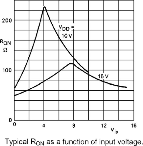
Figure 2 also shows that Ron is lower and varies less when the higher supply voltage is used; since these are enhancement FETs the on-resistance decreases as the available control voltage increases. If you want the best linearity then always use the maximum rated supply voltage.
Since Ron is not very linear, the smaller its value the better. The 4016 Ron is specified as 115 Ω typical, 350 Ω max, over the range of input voltages and with a 15 V supply. The 4066 is a version of the 4016 with lower Ron, 60 Ω typical, 175 Ω max under the same conditions. This option can be very useful both in reducing distortion and improving offness, and in most cases there is no point in using the 4016. The performance figures given below assume the use of the 4066 except where stated.
CMOS gates in voltage mode
Figure 3 shows the simplest and most obvious way of switching audio on and off with CMOS analog gates. This series configuration is in a sense the ‘official’ way of using them; the snag is that by itself it doesn’t work very well.
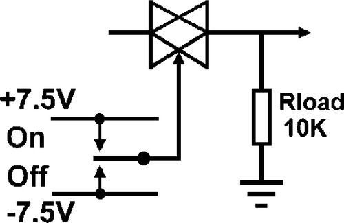
Figure 4 shows the measured distortion performance of the simple series gate using the 4016 type. The distortion performance is a long way from brilliant, exceeding 0.1% just above 2 V r.m.s. These tests, like most in this section, display the results for a single sample of the semiconductor in question. Care has been taken to make these representative, but there will inevitably be some small variation in parameters like Ron. This may be greater when comparing the theoretically identical products of different manufacturers.
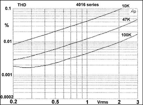
Replacing the 4016 gate with a 4066 gives a reliable improvement due to the lower Ron. THD at 2 V r.m.s. (10 K load) has dropped to a third of its previous level. There seems to be no downside to using 4066 gates instead of the more common and better-known 4016, and they are used exclusively from this point on.
The distortion is fairly pure second harmonic, except at the highest signal levels where higher-order harmonics begin to intrude. This is shown in Figures 5 and 6 by the straight line plots beginning to bend upwards above 2 V r.m.s.
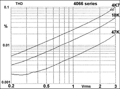

Analogue gate distortion is flat with frequency from 10 Hz up to 30 kHz at least, and so no plots of THD versus frequency are shown; they would merely be a rather uninteresting set of horizontal lines.
This circuit (Figure 3) gives poor offness when off, and poor distortion when on. The offness is limited by the stray capacitance in the package feeding through into the relatively high load impedance. If this is 10 K the offness is only − 48 dB at 20 kHz, which would be quite inadequate for many applications. The load impedance could be reduced below 10 K to improve offness – for example, 4 K7 offers about a 7 dB improvement – but this degrades the distortion, which is already poor at 0.055% for 3 V r.m.s., to 0.10%. Using 4066 gates instead of 4016 does not improve offness in this configuration. The internal capacitance that allows signals to leak past the gate seems to be the same for both types.
The maximum signal level that can be passed through (or stopped) is limited by the CMOS supply rails and conduction of the protection diodes. While it would in some cases be possible to contrive a bootstrapped supply to remove this limitation, it is probably not a good route to head down.
Figure 8 above shows a CMOS three-way switch. When analogue gates are used as a multi-way switch, the offness problem is much reduced, because capacitative feedthrough of the unwanted inputs is attenuated by the low Ron looking back into the (hopefully) low impedance of the active input, such as an opamp output. If this is not the case then the crosstalk from nominally off inputs can be serious. In this circuit the basic poor linearity is unchanged, but since the crosstalk problem is much less, there is often scope for increasing the load impedance to improve linearity. This makes Ron a smaller proportion of the total resistance. The control voltages must be managed so that only one gate is on at a time, if there is a possibility of connecting two opamp outputs together.
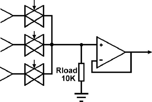
It may appear that if you are implementing a true changeover switch, which always has one input on, the resistor to ground is redundant, and just a cause of distortion. Omitting it is however very risky, because if all CMOS gates are off together even for an instant, there is no DC path to the opamp input and it will register its displeasure by snapping its output to one of the rails. This does not sound nice.
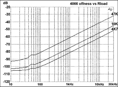
Figure 9 shows the offness of a changeover system, for two types of FET-input opamps. The offness is much improved to − 87 dB at 20 kHz, an improvement of 40 dB over the simple series switch; at the high-frequency end however it still degrades at the same rate of 6 dB/octave. It is well-known that the output impedance of an op-amp with negative feedback increases with frequency at this rate, as the amount of internal gain falls, and this effect is an immediate suspect. However, there is actually no detectable signal on the opamp output, (as shown by the lowest trace in Figure 9) and is also not very likely that two completely different opamps would have exactly the same output impedance. I was prepared for a subtle effect, but the true explanation is that the falling offness is simply due to feedthrough via the internal capacitance of the analogue gate.

It now remains to explain why the OPA2134 apparently gives better offness in the flat low-frequency region. In fact it does not; the flat parts of the trace represent the noise floor for that particular opamp. The OPA2134 is a more sophisticated and quieter device than the TL072, and this is reflected in the lower noise floor.
There are two linearity problems. Firstly, the on-resistance itself is not totally linear. Second, and more serious, the on-resistance is modulated when the gates move up and down with respect to their fixed gate voltages.
It will by now probably have occurred to most readers that an on/off switch with good offness can be made by making a changeover switch with one input grounded. This is quite true, but since much better distortion performance can be obtained by using the same approach in current mode, as explained below, I am not considering it further here.
Figure 10 above shows a shunt muting circuit. This gives no distortion in the ‘ON’ state because the signal is no longer going through the Ron of a gate. However the offness is limited by the Ron, forming a potential divider with the series resistor R; the latter cannot be very high in value or the circuit noise will be degraded. There is however the advantage that the offness plot is completely flat with frequency. Note that the ON and OFF states of the control voltage are now inverted.
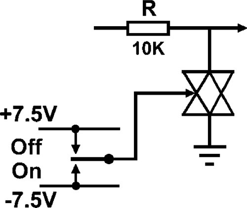
Table 1 below gives the measured results for the circuit, using the 4066. The offness can be improved by putting two or more of these gates in parallel, but since doubling the number N only gives 6 dB improvement, it is rarely useful to press this approach beyond four gates.
CMOS gates in current mode
Using these gates in current mode – usually by defining the current through the gate with an input resistor and dropping it into the virtualearth input of a shunt-feedback amplifier – gives much superior linearity. It removes the modulation of channel resistance as the gate goes up and down with respect to its supply rails, and, in its more sophisticated forms, can also remove the signal voltage limit and improve offness.
Figure 11 shows the simplest version of a current-mode on/off switch, and it had better be said at once that it is a bit too simple to be very useful as it stands. An important design decision is the value of Rin and Rnfb, which are often equal to give unity gain. Too low a value increases the effect of the non-linear Ron, while too high a value degrades offness, as it makes the gate stray capacitance more significant, and also increases Johnson noise from the resistors. In most cases 22 K is a good compromise.
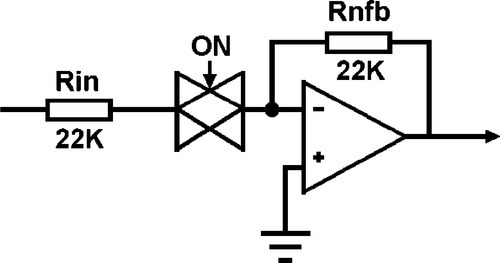
Table 2 gives the distortion for dBu (7.75 V r.m.s.) in/out, and shows that it is now very low compared with voltage-mode switchers working at much lower signal levels; compare with Figures 5 and 6. The increase in THD at high frequencies is due to a contribution from the opamp. However, the offness is pretty poor, and would not be acceptable for most applications. The problem is that with the gate off, the full signal voltage appears at the gate input and crosstalks to the summing node through the package’s internal capacitance. In practical double-sided PCB layouts the inter-track capacitance can usually be kept very low by suitable layout, but the internal capacitance is inescapable.
Table 2
Distortion and offness for 4016 series current-mode switching
| 1 kHz | 10 kHz | 20 kHz | |
| THD via 4016, dBu (%) | 0.0025 | 0.0039 | 0.0048 |
| THD: 4016 shorted, dBu (%) | 0.0020 | 0.0036 | 0.0047 |
| Offness (dB) | − 68 | − 48 | − 42 |

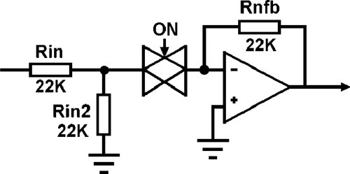
In Figures 11 and 12, the CMOS gate is powered from a maximum of +/− 7.5 V. This means that in Figure 11, signal breakthrough begins at an input of 5.1 V r.m.s. This is much too low for opamps running off their normal rail voltages, and several dB of headroom is lost. Figure 12 shows a partial cure for this. Resistor Rin2 is added to attenuate the input signal when the CMOS gate is off, preventing breakthrough. There is no effect on gain when the gate is on, but the presence of Rin2 does increase the noise gain of the stage.
Series-shunt current mode
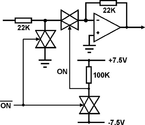
We now extravagantly use two 4016 CMOS gates, as shown in Figure 13.

When the switch is on, the series gate passes the signal through as before; the shunt gate is off and has no effect. When the switch is off the series gate is off and the shunt gate is on, sending almost all the signal at A to ground so that the remaining voltage is very small. The exact value depends on the 4016 specimen and its Ron value, but is about 42 dB below the input voltage. This deals with the offness (by greatly reducing the signal that can crosstalk through the internal capacitance) and also increases the headroom by several dB, as there is now effectively no voltage signal to breakthrough when it exceeds the rails of the series gate.
Two antiphase control signals are now required. An excellent way to generate the inverted control signal is to use a spare analogue gate as an inverter, as shown in Figure 14.
The distortion generated by this circuit can be usefully reduced by using two gates in parallel for the series switching, as in Table 3 below; this gate-doubling reduces the ratio of the variable Ron to the fixed series resistor and so improves the linearity. Using two in parallel is sufficient to render the distortion negligible. (The higher distortion figures at 10 and 20 kHz are due to distortion generated by the TL072 opamp used in the measurements.)
Table 3
Distortion and offness for 4016 series-shunt current-mode switching
| 1 kHz | 10 kHz | 20 kHz | |
| THD via 4016 × 1, + 20 dBu | 0.0016% | 0.0026% | 0.0035% |
| THD via 4016 × 2, + 20 dBu | 0.0013% | 0.0021% | 0.0034% |
| THD 4016 shorted, dBu | 0.0013% | 0.0021% | 0.0034% |
| Offness 4016 × 1 (dB) | − 109 | − 91 | − 86 |
| Offness 4016 × 1, J111 (dB) | Less than − 116 | − 108 | − 102 |
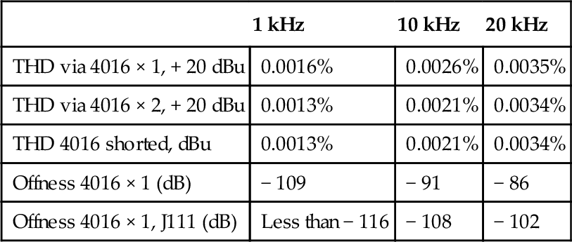
As before the input and output levels are + 20 dBu, well above the nominal signal levels expected in opamp circuitry; measurements taken at more realistic levels would show only noise.
Discrete FETs have lower Ron than analogue gates. If a J111 JFET is used as the shunt switching element the residual signal at A is further reduced, to about 60 dB below the input level, with a consequent improvement in offness, demonstrated by the final entry in Table 3. This could also be accomplished by using two or more CMOS gates in parallel for the shunt switching.
There is more on discrete FETs in Part Two of this article (Chapter 13).
Control voltage feedthrough in CMOS gates
When an analogue gate changes state, some energy from the control voltage passes into the audio path via the gate-channel capacitance of the switching FETs, through internal package capacitances, and through any stray capacitance designed into the PCB. Since the control voltages of analogue gates move snappily, due the internal inverters, this typically puts a click rather than a thump into the audio. Attempts to slow down the control voltage going into the chip with RC networks are not likely to be successful for this reason. In any case, slowing down the control voltage change simply converts a click to a thump; the FET gates are moving through the same voltage range, and the feedthrough capacitance has not altered, so the same amount of electric charge has been transferred to the audio path – it just gets there more slowly.
The only certain way to reduce the effect of transient feedthrough is to soak it up in a lower value of load resistor. The same electric charge is applied to a lower resistor value (the feedthrough capacitance is tiny, and controls the circuit impedance) so a lower voltage appears. Unfortunately reducing the load tends to increase the distortion, as we have already seen; the question is if this is acceptable in the intended application.