Electronic analogue switching, Part II: discrete FETs
Discrete FET switching
Having looked in detail at analogue switching using CMOS gates, and having seen how well they can be made to work, you might be puzzled as to why anyone should wish to perform the same function with discrete FETs. There are at least two advantages in particular applications. Firstly, JFETs can handle the full output range of opamps working from maximum supply rails, so higher signal levels can often be switched directly without requiring opamps to convert between current and voltage mode. Secondly, the direct access to the device gate allows relatively slow changes in attenuation (though still measured in milliseconds, for reasons that will emerge) rather than the rapid on–off action which CMOS gates give as a result of their internal control-voltage circuitry. This is vital in creating mute circuits that essentially implement a fast fade rather than a sharp cut, and so do not generate clicks and thumps by abruptly interrupting the signal.
The downside is that they require carefully-tailored voltages to drive the gates, and these cannot always be conveniently derived from the usual opamp supply rails.
Discrete FETs in voltage mode: the series JFET switch
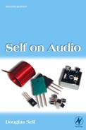
The basic JFET series switching circuit is shown in Figure 1. With the switch open there is no other connection to the gate other than the bootstrap resistor, Vgs is zero, and so the FET is on. When the switch is closed, the gate is pulled down to a sufficiently negative voltage to ensure that the FET is biased off even when the input signal is at its negative limit.
The JFET types J111 and J112 are specially designed for analogue switching and are pre-eminent for this application. The channel on-resistances are low and relatively linear. This is a depletion-mode FET, which requires a negative gate voltage to actively turn it off. The J111 requires a more negative Vgs to ensure it is off, but in return gives a lower Rds(on) which means lower distortion.
The J111, J112 (and J113) are members of the same family – in fact they are same the device, selected for gate/channel characteristics, unless I am much mistaken. Table 1 shows how the J111 may need 10 V to turn it off, but gives a 30 Ω on-resistance or Rds(on) with zero gate voltage. In contrast the J112 needs only 5.0 V at most to turn it off, but has a higher Rds(on) of 50 Ohms. The trade-off is between ease of generating the gate control voltages, and linearity. The higher the Rds(on), the higher the distortion, as this is a non-linear resistance.
Table 1
Characteristic of the J111 FET series
| J111 | J112 | J113 | |
| Vgs(off) min | − 3.0 | − 1.0 | − 0.5 V |
| Vgs(off) max | − 10 | − 5.0 | − 3.0 V |
| Rds(on) | 30 | 50 | 100 |

FET tolerances are notoriously wide, and nothing varies more than the Vgs characteristic. It is essential to take the full range into account when designing the control circuitry.
Both the J111 and J112 are widely used for audio switching. The J111 has the advantage of the lowest distortion, but the J112 can be driven directly from 4000 series logic running from 7.5 V rails, which is often convenient. The J113 appears to have no advantage to set against its high Rds(on) and is rarely used – I have never even seen one.
The circuits below use either J111 or J112, as appropriate. The typical version used is shown, along with typical values for associated components.
Figure 1 has Source and Drain marked on the JFET. In fact these devices appear to be perfectly symmetrical, and it seems to make no difference which way round they are connected, so further diagrams omit this. As JFETs, in practical use they are not particularly static-sensitive.
The off voltage must be sufficiently negative to ensure that Vgs never becomes low enough to turn the JFET on. Since a J111 may require a Vgs of − 10 V to turn it off, the off voltage must be 10 V below the negative saturation point of the driving opamp – hence the − 23 V rail. This is not exactly a convenient voltage, but the rail does not need to supply much current and the extra cost in something like a mixing console is relatively small.
To turn a JFET on, the Vgs must be held at 0 V. That sounds simple enough, but it is actually the more difficult of the two states. Since the source is moving up and down with the signal, the gate must move up and down in exactly the same way to keep Vgs at zero. This is done by bootstrap resistor Rboot in Figure 1. When the JFET is off, d.c. flows through this resistor from the source; it is therefore essential that this path be d.c.-coupled and fed from a low impedance such as an opamp output, as shown in these diagrams. The relatively small d.c. current drawn from the opamp causes no problems.
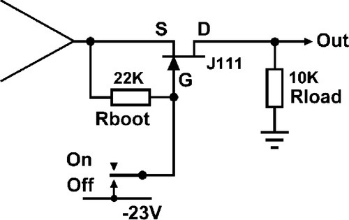
Figure 2 is a more practical circuit using a driver transistor to control the JFET. (If you had a switch contact available, you would presumably use it to control the audio directly.) The pull-up resistor Rc keeps diode D reverse-biased when the JFET is on; this is its sole function, so the value is not critical. It is usually high to reduce power consumption. I have used anything between 47 K and 680 K with success.

Sometimes d.c.-blocking is necessary if the opamp output is not at a d.c. level of 0 V. In this case the circuit of Figure 3 is very useful; the audio path is d.c.-blocked but not the bootstrap resistor, which must always have a d.c. path to the opamp output. Rdrain keeps the capacitor voltage at zero when the JFET is held off.
Figure 4 shows the distortion performance with a load of 10 K. The lower curve is the distortion from the opamp alone; the low THD level should tell you immediately it was a 5532. The signal level was 7.75 V r.m.s. (+ 20 dBu).

Figure 5 shows the distortion performance with heavier loading, from 10 K down to 1 K. As is usual in the world of electronics, heavier loading makes things worse. In this case, it is because the non-linear Ron becomes a more significant part of the total circuit resistance. The signal level was 7.75 V r.m.s. (+ 20 dBu).
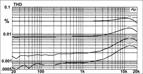
Figure 6 shows the distortion performance with different values of bootstrap resistor. The lower the value, the more accurately the drain follows the source at high audio frequencies, and so the lower the distortion. The signal level was 7.75 V r.m.s. (+ 20 dBu) once again. There appears to be no disadvantage to using a bootstrap resistor of 22 K or so, except in in special circumstances, as explained below.

Two series JFET switches can be simply combined to make a changeover switch, as shown in Figure 7. The valid states are A on, B on, or both off. Both on is not a good option because the two opamps will then be driving each other’s outputs through the JFETs.

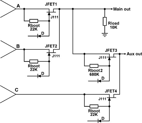
It is possible to cascade FET switches, as in Figure 8, which is taken from a real application. Here the main output is switched between A and B as before, but a second auxiliary output is switched between this selection and another input C by JFET3 and JFET 4. Cascading FET switches in this way removes the need for a buffer opamp between JFET1 and JFET3. The current drawn by the second bootstrap resistor Rboot2 must flow through the Rds(on) of the first FET, and will thus generate a small click. Rboot2 is therefore made as high as possible to minimise this effect, accepting that the distortion performance of the JFET3 switch will be compromised at HF; this was acceptable in the application as the second output was not a major signal path. The bootstrap resistor of JFET4 can be the desirable lower value of 22 K as this path is driven direct from an opamp.
The offness of this type of series FET switch is not usually an issue because it is almost always used in the changeover format, where capacitative crosstalk from the off-JFET is made negligible by the low resistance of the on-JFET. If you simply want to turn a signal off, there are better ways to do it; see below.
The shunt JFET switch
The basic JFET shunt switching circuit is shown in Figure 9. Like the shunt analogue gate mute, it gives poor offness but good linearity in the ON state, so long as its gate voltage is controlled so it never allows the JFET to begin conducting. Its great advantage is that the depletion JFET will be in its low-resistance before and during circuit power-up, and can be used to mute switch-on transients. Switch-off transients can also be effectively muted if the drive circuitry is configured to turn on the shunt FETs as soon as the mains disappears, and keep them on until the various supply rails have completely collapsed.
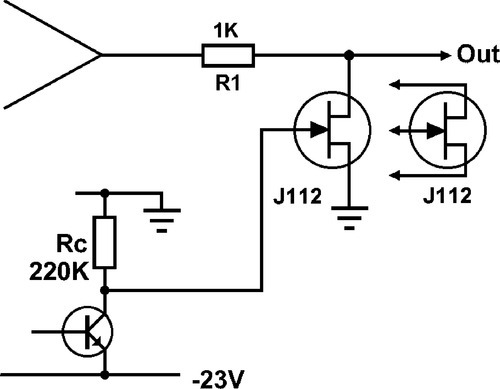
The circuit of Figure 9 was used to mute the turn-on and turn-off transients of a hifi preamplifier. Since this is an output that is likely to drive a reasonable length of cable, with its attendant capacitance, it is important to keep R1 as low as possible, to minimise the possibility of a drooping treble response. This means that the Rds(on) of the JFET puts a limit on the offness possible. The output series resistor R1 is normally in the range 47–100 Ω, when it has as its only job the isolation of the output opamp from cable capacitance. Here it has a value of 1 K, which is a distinct compromise. The muting obtained with 1 K was not quite enough so two J111s were used in parallel, giving a further − 6 dB of attenuation, and yielding in total − 33 dB across the audio band, which was sufficient to render the transients inaudible. The offness is not frequency dependent as the impedances are all low and so stray capacitance is irrelevant.
Discrete FETs in current mode
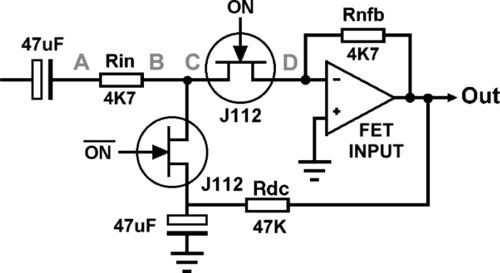
JFETs can be used in the current mode, just as for analogue gates. Figure 10 shows the basic muting circuit, with series FET switching only. Ring prevents breakthrough. The stage as shown has less than unity gain; this can be corrected by increasing Rnfb.
Soft JFET muting: crosstalk/linearity trade-off
When switching audio signals, a instantaneous cut of the signal is sometimes not what is required. When a non-zero audio signal is abruptly interrupted there is bound to be a click. Perhaps surprisingly, clever schemes for making the instant of switching coincide with a zero-crossing give little improvement. There may no longer be a step-change in level, but there is still a step-change in slope and the ear once more interprets this discontinuity as a click.
What is really required is a fast-fade over about 10 ms. This is long enough to prevent clicks, without being so slow that the timing of the event becomes sloppy. This is normally only an issue in mixing consoles, where it is necessary for things to happen in real time. Such fast-fade circuits are often called ‘mute blocks’ to emphasise that they are more than just simple on–off switches. Analogue gates cannot be slowly turned on and off due to their internal circuitry for control-voltage generation. Therefore discrete JFETs must be used. Custom chips to perform this function have been produced, but the ones I have evaluated have been expensive, single-source, and give less than startling results for linearity and offness. This situation is of course subject to change.
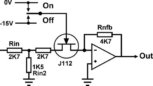
In designing a mute bloc, we want low distortion and good offness at the same time, so the series-shunt configuration, which proved highly effective with CMOS analogue gates, is the obvious choice. The basic circuit is shown in Figure 13. A small capacitor C is usually required to ensure HF stability, (Figure 14) due to the FET capacitances hanging on the virtual-earth node at D.

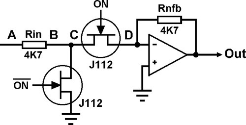

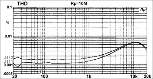
The control voltages to the series and shunt JFETs are complementary as before, but now they can be slowed down by RC networks to make the operation gradual, as shown in Figure 14. The exact way in which the control voltages overlap is easy to control, but the Vgs/resistance law of the FET is not (and is about the most variable FET parameter there is) and so the overlap of FET conduction is rather variable. However, I should say at once that this system does work, and works well enough to go in top-notch mixing consoles. The distortion performance is shown in Figure 15. As you go into the muted condition the series JFET turns off and the shunt JFET turns on, and if the overlap gets to be too much in error, the following bad things can happen:
1. If the shunt FET turns on too early, while the series JFET is still mostly on, a low-resistance path is established from the opamp virtual-earth point to ground, causing a large but brief rise in stage noise gain. This produces a ‘chuff’ of noise at the output as muting occurs.
2. If the shunt FET turns on too late, so the series JFET is mostly off, the large signal voltage presented to the series FET causes visibly serious distortion. I say ‘visibly’ because it is well-known that even quite severe distortion is not obtrusive if it occurs only briefly. The transition here is usually fast enough for this to be the case; it would however not be a practical way to generate a slow fade. The circuit of Figure 14 generates no audible distortion and only a very small chuff.
The drive circuitry
The mute bloc requires two complementary drive voltages, and these are easily generated from 4000-series CMOS running from ± 7.5 V rails. NAND gates are shown here as they are convenient for interfacing with other bits of control logic, but any standard CMOS output can be used. It is vital that the JFET gates get as close to 0 V as possible, ensuring that the series gate is fully on and gives minimum distortion, so the best technique is to and use diodes to clamp the gates to 0 V. Thus, in Figure 14, when the mute bloc is passing signal, the signal from NAND gate A is high, so D1 is reverse-biased and the series JFET TR1 gate is held at 0 V by R1, keeping it on. (The role of Rp will be explained in a moment) Meanwhile, D2 is conducting as the NAND-gate output driving it is low, so the shunt JFET TR2 gate is at about − 7 V and it is firmly switched off. This voltage is more than enough to turn off a J112, but cannot be guaranteed to turn off a J111, which may require − 10 V (See Table 1). This is one reason why the J112 is more often used in this application – it is simpler to generate the control voltages. When the mute bloc is off, the conditions are reversed, with the output of A low, turning off TR1, and the output of B high, turning on TR2.
Reducing THD by on-biasing
The distortion generated by this circuit bloc is of considerable importance, because if the rest of the audio path is made up of 5532 opamps – which is likely in professional equipment – then this stage can generate more distortion than the rest of the signal path combined, and dominate this aspect of the performance. It is therefore worth examining any way of increasing the linearity.
We have already noted that to minimise distortion, the series JFET should be turned on as fully as possible to minimise the value of the non-linear Rds(on). When a JFET has a zero gate-source voltage, it is normally considered fully on. It is, however, possible to turn it even more on than this.
The technique is to put a small positive voltage on the gate, say about 200–300 mV. This further reduces the Rds(on) in a smoothly continuous manner, without forward biasing the JFET gate junction and injecting d.c. into the signal path. This is accomplished in Figure 14 by the simple addition of Rp, which allows a small positive voltage to be set up across the 680 K resistor R1. The value of Rp is usually in the 10–22 MΩ range, for the circuit values shown here.
Care is needed with this technique, because if temperatures rise the JFET gate diode may begin to conduct after all, and d.c. will leak into the signal path, causing thumps and bangs. In my experience 300 mV is about the upper safe limit for equipment that gets reasonably warm internally, i.e. about 50 °C. Caution is the watchword here, for unwanted transients are much less tolerable than slightly increased distortion.
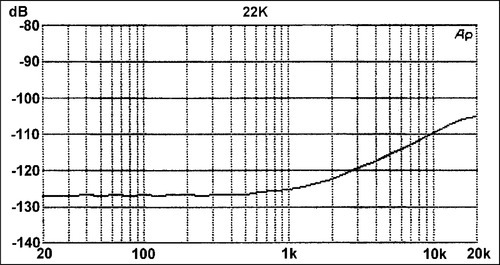
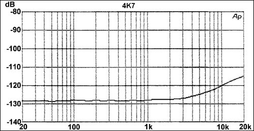
As with analogue CMOS gates, the choice of the resistors Rin and Rnfb that define the magnitude of the signal currents is an important matter. Figures 16 and 17 show the performance of the circuit is affected by using values of 4 K7 and 22 K. Usually 4 K7 would be the preferred value; choosing 22 K as the value makes the noise floor higher, as well as the signal leakage. Values below 4 K7 are not usual as distortion will increase, as the JFET Rds(on) becomes a larger part of the total resistance in the circuit. The loading effect of Rin on the previous stage must also be considered.
Layout and offness
The offness of this circuit is extremely good, providing certain precautions are taken in the physical layout. In Figure 18, there are two possible crosstalk paths that can damage the offness. The path C–D, through the internal capacitances of the series JFET, is rendered innocuous as C is connected firmly to ground by the shunt JFET. However, point A is still alive with full amplitude signal, and it is the stray capacitance from A to D that defines the offness at high frequencies.
Given the finite size of Rin, it is often necessary to extend the PCB track B–C to get A far enough from D. This is no problem if done with caution. Remember that the track B–C is at virtual earth when the mute bloc is on, and so vulnerable to capacitative crosstalk from other signals straying into the area.
Dealing with the d.c.
The circuits shown so far have been stripped down to their bare essentials to get the basic principles across. In reality, things are (surprise) a little more complicated. Opamps have non-zero offset and bias voltages and currents, and if not handled properly these will lead to thumps and bangs. There are several issues:
1. If there is any d.c. voltage at all passed on from the previous stage, this will be interrupted along with the signal, causing a click or thump. The foolproof answer is of course a d.c. blocking capacitor, but if you are aiming to remove all capacitors from the signal path, you may have a problem d.c. servos can partly make up the lack, but since they are based on opamp integrators they are no more accurate than the opamp, while d.c. blocking is totally effective.
2. The offset voltage of the opamp. If the noise gain is changed when the mute operates (which it is) the changing amplification of this offset will change the d.c. level at the output. The answer is shown in Figure 18. The shunt FET is connected to ground via a blocking capacitor to prevent DC gain changes. This capacitor does not count as ‘being in the signal path’ as audio only goes through it when the circuit is muted. Feedback of the opamp offset voltage through Rdc to this capacitor renders it innocuous.
3. The input bias and offset currents of the opamp. These are potentially much more of a problem and are best dealt with by using JFET opamps such as the OPA2134, where the bias and offset currents are negligible at normal equipment temperatures.
Soft changeover circuit
This circuit (Figure 19) is designed to give a soft changeover between two inputs – in effect a fast crossfade. It is the same mute block but with two separate inputs, either or both of which can be switched on. The performance at + 20 dBu in/out is summarised in Table 2.

Table 2
Performance of the series-shunt JFET mute circuit in Figure 14
| 1 kHz | 10 kHz | 20 kHz | |
| THD + 20 dBu (%) | 0.0023 | 0.0027 | 0.0039 |
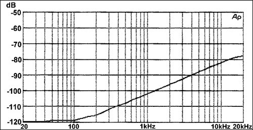
| Offness (dB) | − 114 | − 109 | − 105 |

The THD increase at 20 kHz is due to the use of a TL072 as the opamp. J112 JFETs are used in all positions.
This circuit is intended for soft-switching applications where the transition between states is fast enough for a burst of increased distortion to go unnoticed. It is not suitable for generating slow crossfades in applications like disco mixers, as the exact crossfade law is not very predictable.
Control voltage feedthrough in JFETs
All discrete FETs have a small capacitance between the gate and the device channel, so changes in the gate voltage will therefore cause a charge to be transferred to the audio path, just as for CMOS analogue gates. As before, slowing down the control voltage change tends to give a thump rather than a click to a thump; the same amount of electric charge has been transferred to the audio path, but more slowly. Lowering the circuit impedance reduces the effects of feedthrough, but can only be taken so far before distortion begins to increase as the non-linear Rds(on) of the JFET becomes a greater part of the total circuit resistance.