Distortion in power amplifiers, Part I: the sources of distortion
For many years I felt that the output stages of power amplifiers presented very great possibilities for creative design, and I actually got round to exploring some of them. The hybrid bipolar-FET output stage, also collected in this volume, was one of them. One of the first difficulties I met was the problem of determining how much of the total distortion was due to the output stage, and how much was being produced in the small-signal sections. This latter contribution turned out to be larger and more important than I expected. Very little reliable information appeared to exist on amplifier distortion, and I found myself embarked on a major effort to track down all the sources of distortion in the typical solid-state power amplifier. The initial investigations were not very illuminating, until I realised that changing a component value in the typical power amplifier circuit very often alters two or more distortion mechanisms simultaneously, making the results hard to interpret. I was sitting in my armchair late one Spring night when the full force of this struck home, and thereafter I devised ways to simulate or measure the distortion mechanisms in isolation. This approach is well-illustrated in Parts 2 and 3 of the series, dealing with the input pair and the Voltage-Amplifier Stage, respectively.
Things then began to fall into place, and one day I put together all the various minor and, apparently insignificant, improvements I had made to the utterly conventional amplifier circuit I had started with. The distortion was exhilaratingly low, stability was good, and I soon felt that I could write a pretty comprehensive guide to distortion and power amplifier design. Electronics World were good enough to give me all the space I asked for, and I believe I succeeded; here, in eight chapters, is the result.
It seems surprising that in a world which can build the Space Shuttle and detect the echoes of the birth of the universe, we still have to tolerate distortion in power amplifiers. Leafing through recent reviews and specifications shows claims for full-power total harmonic distortion ranging more than three orders of magnitude between individual designs, a wider range than any other parameter.
Admittedly the higher end of this range is represented by subjectivist equipment that displays dire linearity, presumably with the intention of implying that other nameless audio properties have been given priority over the mundane business of getting the signal from input to output without bending it.
Given the juggernaut rate of progress in most branches of electronics this seems to me anomalous, and especially notable in view of the many advanced analogue techniques used in op-amp design; after all power amps are only op-amps with boots on. One conclusion seems inescapable: a lot of power amplifiers generate much more distortion than they need to.
This series attempts to show exactly why amplifiers distort, and how to stop them doing it, culminating in a practical design for an ultra-linear amplifier. It should perhaps be said at the outset that none of this depends on excessively high levels of negative feedback. Many of the techniques described here are also entirely applicable to discrete op-amps, headphone drivers, and similar circuit blocks. Since we are almost in the twenty-first century I have ignored valve amplifiers.
Since mis-statements and confusions are endemic to audio, I have based these articles almost entirely on my own experimental work backed up with spice circuit simulation; much of the material relates specifically to bipolar transistor output stages, though a good deal is also relevant to mosfet amplifiers. Some of the statements made may seem controversial, but I believe they are all correct. If you think not, please tell me, but only if you have some real evidence to offer.
The fundamental reason why amplifier distortion persists is, of course, because it is a difficult technical problem to solve. A Science proverbially becomes an Art when there are more than seven variables, and since it will emerge that there are seven major distortion mechanisms to the average amplifier, we would seem to be nicely balanced on the boundary of the two cultures. Given so many significant sources of unwanted harmonics, overlaid and sometimes partially cancelling, sorting them out is a nontrivial task.
Make your amplifier as linear as possible before applying NFB has long been a cliche, (one that conveniently ignores the difficulty of running a high gain amp without any feedback) but virtually no dependable advice on how to perform this desirable linearisation has been published. The two factors are the basic linearity of the forward path, and the amount of negative feedback applied to further straighten it out. The latter cannot be increased beyond certain limits or high-frequency stability is put in peril, whereas there seems no reason why open-loop linearity could not, in principle, be improved without limit, leading us to the Holy Grail of the distortionless amplifier. This series therefore takes as its prime aim the understanding and improvement of open-loop linearity. As it proceeds we will accrete circuit blocks to culminate in two practical amplifier designs that exploit the techniques presented here.
How an amplifier (really) works
Figure 1 shows the usual right trusty and well-beloved power amp circuit drawn as standard is possible. Much has been written about this configuration, though its subtlety and quiet effectiveness are usually overlooked, and the explanation below therefore touches on several aspects that seem to be almost unknown. It has the merit of being docile enough to be made into a workable amplifier by someone who has only the sketchiest of notions as to how it works.
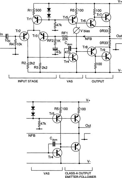
The input differential pair implements one of the few forms of distortion cancellation that can be relied upon to keep working in all weathers. This is because the transconductance of the input pair is determined by the physics of transistor action rather than matching of variable parameters such as beta; the logarithmic relation between Ic and Vbe is proverbially accurate over some eight or nine decades of current variation.
The voltage signal at the voltage amplifier stage (hereafter VAS) transistor base is typically a couple of millivolts, looking rather like a distorted triangle wave. Fortunately the voltage here is of little more than academic interest, as the circuit topology essentially consists of a transconductance amp (voltage-difference input to current output) driving into a transresistance (current-to-voltage converter) stage. In the first case the exponential Vbe/Ic law is straightened out by the differential-pair action, and in the second the global (overall) feedback factor at LF is sufficient to linearise the VAS, while at HF shunt negative feedback (hereafter NFB) through Cdom conveniently takes over VAS-linearisation while the overall feedback factor is falling. The behaviour of Miller dominant-pole compensation in this stage is exceedingly elegant, and not at all just a case of finding the most vulnerable transistor and slugging it. As frequency rises and Cdom begins to take effect, negative feedback is no longer applied globally around the whole amplifier, which would include the higher poles, but instead is seamlessly transferred to a purely local role in linearising the VAS. Since this stage effectively contains a single gain transistor, any amount of NFB can be applied to it without stability problems.
The amplifier operates in two regions; the LF, where open-loop gain is substantially constant, and HF, above the dominant-pole breakpoint, where the gain is decreasing steadily at 6 dB/octave. Assuming the output stage is unity-gain, three simple relationships define the gain in these two regions:
At least one of the factors that set this (beta) is not well-controlled and so the LF gain of the amplifier is to a certain extent a matter of potluck; fortunately this doesn’t matter as long as it is high enough to give a suitable level of NFB to eliminate LF distortion. The use of the word ‘eliminate’ is deliberate, as will be seen later. Usually the LF gain, or HF local feedback-factor, is made high by increasing the effective value of the VAS collector impedance Rc, either by the use of a currentsource collector-load, or by some form of bootstrapping.
The other important relations are:
where ω = 2πf.
In the HF region, things are distinctly more difficult as regards distortion, for while the VAS is locally linearised, the global feedback-factor available to linearise the input and output stages is falling steadily at 6 dB/octave. For the time being we will assume that it is possible to define an HF gain (say N dB at 20 kHz) which will assure stability with practical loads and component variations. Note that the HF gain, and therefore both HF distortion and stability margin, are set by the simple combination of the input stage transconductance and one capacitor, and most components have no effect on it at all.
It is often said that the use of a high VAS collector impedance provides a current drive to the output devices, often with the implication that this somehow allows the stage to skip quickly and lightly over the dreaded crossover region. This is a misconception – the collector impedance falls to a few kΩ at HF, due to increasing local feedback through Cdom. In any case it is very doubtful if true current drive would be a good thing since calculation shows that a low-impedance voltage drive minimises distortion due to beta-unmatched output halves,1 and it certainly eliminates distortion mechanism four described later.
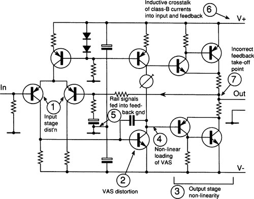
The seven distortions
In the typical amplifier THD is often thought to be simply due to the Class-B nature of the output stage, which is linearised less effectively as the feedback factor falls with increasing frequency. However the true situation is much more complex as the small-signal stages can generate significant distortion in their own right in at least two different ways. This can easily exceed the output stage distortion at high frequencies. It seems inept to allow this to occur given the freedom of design possible in the small-signal section.
Include all the ills that a class-B stage is prone to and then there are seven major distortion mechanisms.
Distortion in power amplifiers arises from:
1. Non-linearity in the input stage. If this is a carefully-balanced differential pair then distortion is typically only measurable at HF, rises at 18 dB/octave, and is almost pure third harmonic.
If the input pair is unbalanced (which from published circuitry it usually is) then the HF distortion emerges from the noise floor earlier. As frequency increases, it rises at 12 dB/octave as it is mostly second harmonic.
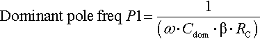
2. Non-linearity in the voltage amplifier stage surprisingly does not always figure in the total distortion. If it does, it remains constant until the dominant-pole frequency P1 is reached, and then rises at 6 dB/octave. With the configurations discussed here, it is always second harmonic.
Usually the level is very low due to linearising negative feedback through the dominant-pole capacitor. Hence if you crank up the local VAS open-loop gain, for example by cascoding or putting more currentgain into the local VAS/Cdom loop, and attend to mechanism four below, you can usually ignore VAS distortion.
3. Non-linearity in the output stage, which is naturally the obvious source. This, in a Class-B amplifier, will be a complex mix of largesignal distortion and crossover effects, the latter generating a spray of high-order harmonics, and in general rising at 6 dB/octave as the amount of negative feedback decreases. Large-signal THD worsens with 4 Ω loads and worsens again at 2 Ω. The picture is complicated by dilatory switch-off in the relatively slow output devices, ominously signalled by supply current increasing in the top audio octaves.
4. Loading of the VAS by the non-linear input impedance of the output stage. When all other distortion sources have been attended to, this is the limiting distortion factor at LF (say below 2 kHz). It is simply cured by buffering the VAS from the output stage. Magnitude is essentially constant with frequency, though overall effect in a complete amplifier becomes less as frequency rises and feedback through Cdom starts to linearise the VAS.
5. Non-linearity caused by large rail-decoupling capacitors feeding the distorted signals on the supply lines into the signal ground. This seems to be the reason many amplifiers have rising THD at low frequencies. Examining one commercial amplifier kit, I found that rerouting the decoupler ground-return reduced THD at 20 Hz by a factor of three.
6. Non-linearity caused by induction of Class-B supply currents into the output, ground, or negative-feedback lines. This was highlighted by Cherry3 but seems to remain largely unknown; it is an insidious distortion that is hard to remove, though when you know what to look for on the THD residual, it is fairly easy to identify. I suspect that a large number of commercial amplifiers suffer from this to some extent.
7. Non-linearity resulting from taking the NFB feed from slightly the wrong place near where the power-transistor Class-B currents sum to form the output. This may well be another common defect.
Having set down what Mao might have called The Seven Great Distortions – Figure 2 shows the location of these mechanisms diagrammatically – we may pause to put to flight a few Paper Tigers. The first is common-mode distortion in the input stage, a spectre that tends to haunt the correspondence columns. Since it is fairly easy to make an amplifier with less than < 0.00065% THD (1 kHz) without paying any special attention to this, it cannot be too serious a problem. A more severe test is to apply the full output voltage as a common-mode signal, by the amplifier as a unity-gain voltage-follower. If this is done using a model (see below for explanation) small-signal version of Figure 1, with suitable attention to compensation, then it yields less than 0.001% at 8 V r.m.s. across the audio band. It therefore appears that the only real precaution required against common-mode distortion is to use a tail current-source for the input pair.
The second distortion conspicuous by its absence in the list is the injection of distorted supply-rail signals directly into the amplifier circuitry. Although this putative mechanism has received a lot of attention,4 dealing with Distortion five above by proper grounding seems to be all that is required . . . Once again, if triple-zero THD can be attained using simple unregulated supplies and without specifically addressing power supply rejection ratio, (which it reliably can be) then much of the work done on regulated supplies may be of doubtful utility. However, PSRR does need some attention if the hum/noise performance is to be of the first order.
A third mechanism of doubtful validity is thermal distortion, allegedly induced by parameter changes in semiconductor devices whose instantaneous power dissipation varies over a cycle. This would presumably manifest itself as a distortion increase at very low frequencies, but it simply does not seem to happen. The major effects would be expected in Class-B output stages where dissipation can vary wildly over a cycle. However drivers and output devices have relatively large junctions with high thermal inertia. Low frequencies are of course also where the NFB factor is at its maximum.
To return to our list of the unmagnificent seven, note that only Distortion three is directly due to O/P stage non-linearity, though numbers 4–7 all result from the Class-B nature of the typical output stage.
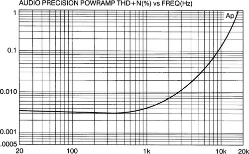
The performance
The THD curve for the standard amplifier is shown in Figure 3. As usual the distortion increases with frequency and, as we shall see later, would give grounds for suspicion if it did not. The flat part of the curve below 500 Hz represents non-frequency-sensitive distortion rather than the noise floor, which for this case is at about the 0.0005% level. Above 500 Hz the distortion rises at an increasing rate, rather than a constant number of dB/octave, due to the combination of Distortions 1,2,3 and 4. (In this case Distortions 5,6 and 7 have been carefully eliminated to keep things simple. This is why the distortion performance looks good already, and the significance of this should not be overlooked.) It is often written that having distortion constant across the audio band is a good thing. This is a most unhappy conclusion as the only practical way to achieve this with a Class-B amplifier is to increase the distortion at LF, for example by allowing the VAS to distort significantly.
It should now be clear why it can be hard to wring linearity out of a snake-pit of contending distortions. A circuit-value change is likely to alter at least two of the distortion mechanisms, and probably change the openloop gain as well. In the coming articles I shall demonstrate how each of these mechanisms can be measured and manipulated separately.
Determining open-loop linearity
Improving something demands its measurement, and so it is essential to examine the open-loop linearity of typical power-amp circuits. This cannot in general be done directly, so it is necessary to measure the NFB factor and calculate open-loop distortion from the usual closedloop data. It is assumed that the closed-loop gain is fixed by operational requirements.
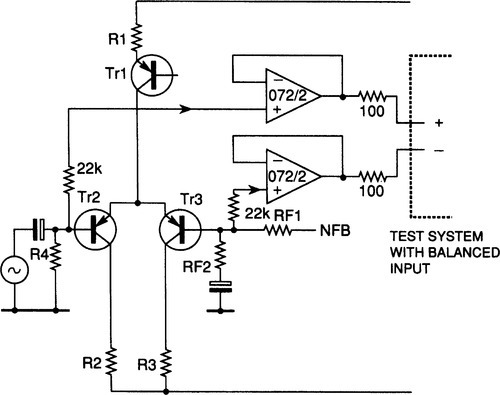
Finding the feedback-factor is at first sight difficult, as it means determining the open-loop gain. The standard methods for measuring op-amp open-loop gain involve breaking feedback-loops and manipulating closedloop gains, procedures that are likely to send the average power-amplifier into fits. However, the need to measure this parameter is inescapable, as a typical circuit modification – e.g. changing the value of R2 – will change the open-loop gain as well as the linearity, and to prevent total confusion it is necessary to keep a very clear idea of whether the observed change is due to an improvement in open-loop linearity or merely because the open-loop gain has risen. It is wise to keep a running check on the feedback-factor as work proceeds, and so the direct method of open-loop gain measurement shown in Figure 4 was evolved.
Direct open-loop gain measurement
Since the amplifier shown in Figure 1 is a differential amplifier, its openloop gain is simply the output divided by the voltage difference between the inputs. If the output voltage is kept effectively constant by providing a swept-frequency constant voltage at the + ve input, then a plot of open-loop gain versus frequency is obtained by measuring the error-voltage between the inputs, and referring this to the output level. This yields an upside-down plot that rises at HF rather than falling, as the differential amplifier requires more input for the same output as frequency increases, but the method is so quick and convenient that this can be lived with. Gain is plotted in dB with respect to the chosen output level (+ 16 dBu in this case) and the actual gain at any frequency can be read off simply by dropping the minus sign. Figure 5 shows the plot for the amplifier in Figure 1.
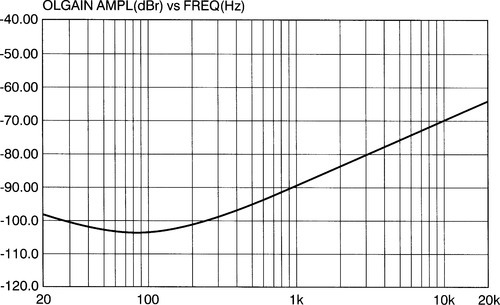
The HF-region gain slope is always 6 dB/octave unless you are using something special in the way of compensation and, by the Nyquist rules, must continue at this slope until it intersects the horizontal line representing the feedback factor provided that the amplifier is stable. In other words, the slope is not being accelerated by other poles until the loop gain has fallen to unity, and this provides a simple way of putting a lower bound on the next pole P2; the important P2 frequency (which is usually some-what mysterious) must be above the intersection frequency if the amplifier is seen to be stable.
Given test gear with a sufficiently high common-mode-rejection-ratio balanced input, the method of Figure 4 is simple; just buffer the differential inputs from the cable capacitance with TL072 buffers, placing negligible loading on the circuit if normal component values are used. Be particularly wary of adding stray capacitance to ground to the − ve input, as this directly imperils amplifier stability by adding an extra feedback pole. Short wires from power amplifier to buffer IC can usually be unscreened as they are driven from low impedances.
The test gear input CMRR defines the maximum open-loop gain measurable; I used an Audio Precision System-1 without any special alignment of CMRR. A calibration plot can be produced by feeding the two buffer inputs from the same signal; this will probably be found to rise at 6 dB/octave, being set by the inevitable input asymmetry. This must be low enough for amplifier error signals to be above it by at least 10 dB for reasonable accuracy. The calibration plot will flatten out at low frequencies, and may even show an LF rise due to imbalance of the test gear input-blocking capacitors; this can make determination of the lowest pole P1 difficult, but this is not usually a vital parameter in itself.
Model amplifiers
The first two distortions on the list can dominate amplifier performance and need to be studied without the complications introduced by a Class-B output stage. This can be done by reducing the circuit to a model amplifier that consists of the small-signal stages alone, with a very linear Class A emitter-follower attached to the output to allow driving the feedback network. Here ‘small-signal’ refers to current rather than voltage, as the model amplifier should be capable of giving a full power-amp voltage swing, given sufficiently high rail voltages. From Figure 2 it is clear that this will allow study of Distortions 1 and 2 in isolation, and using this approach it will prove relatively easy to design a small-signal amplifier with negligible distortion across the audio band. This is the only sure foundation on which to build a good power amplifier.
A typical plot combining Distortions 1 and 2 from a model amp is shown in Figure 6, where it can be seen that the distortion rises with an accelerating slope, as the initial rise at 6 dB/octave from the VAS is contributed to and then dominated by the 12 dB/octave rise in distortion from an unbalanced input stage.

The model can be powered from a regulated current-limited PSU to cut down the number of variables, and a standard output level chosen for comparison of different amplifier configurations. The rails and output level used for the results in these articles was ± 15 V and + 16 dBu. The rail voltages can be made comfortably lower than the average amplifier HT rail, so that radical bits of circuitry can be tried out without the creation of a silicon cemetery around your feet. It must be remembered that some phenomena such as input-pair distortion depend on absolute output level, rather than the proportion of the rail voltage used in the output swing, and will be worse by a mathematically predictable amount when the real voltage swings are used. The use of such model amplifiers requires some caution, and cannot be applied to bipolar output stages whose behaviour is heavily influenced by the sloth and low current gain of the power devices. As another general rule, if it is not possible to lash on a real output stage quickly and get a stable and workable power amplifier; the model may be dangerously unrealistic.