
Power amplifier input currents and their troubles
This article grew out of some work that I was doing for a well-known amplifier company. I had produced a nice low-distortion design, which was to a great extent a straightforward application of the Blameless amplifier design methodology described in the Distortion In Power Amplifier series. However, a late change to the specification of the product – a thing not wholly unknown in the world of audio engineering – meant that a resistive network had to be added immediately before the power amplifier stage. The effective source resistance of the network was, if memory serves, 2 kΩ, and when you have perused the following article you will understand that the effects on both the hum and distortion performance were most unwelcome.
Adding a 5532 buffer stage between resistive network and amplifier would have been a quick fix, but running another op-amp from the very limited amount of ± 15 V power available was going to be awkward, and PCB area in the right place was also a very scarce resource. The 5532 is a low-noise op-amp, but it is not as quiet as the pair of discrete transistors in the power amplifier input section, and the overall noise performance would definitely have suffered.
It was therefore time to look a little more closely at the exact mechanisms by which the source resistance was causing trouble, in the hope that more elegant ways of retrieving the original performance could be found. They were, and this chapter tells the story of how those mechanisms were uncovered, and rendered less troublesome.
When power amplifiers are measured, the input is normally driven from a low impedance signal generator. Some testgear, such as the much-loved Audio Precision System-1, has selectable output impedance options of 50, 150, and 600 Ω. The lowest value available is almost invariably used because (1) it minimises the Johnson noise from the source resistance; (2) it minimises level changes due to loading by the amplifier input impedance.
This is all very sensible, and exactly the way I do it myself – 99% of the time. There is however two subtle effects that can be missed if the amplifier is always tested this way. These are: distortion caused by the non-linear input currents drawn by the typical power amplifier, and hum caused by ripple modulation of the same input currents.
Note that this is not the same effect as the excess distortion produced by FET-input opamps when driven from significant source impedances; this is due to their non-linear input capacitances to the IC substrate, and has no equivalent in power amplifiers made of discrete transistors.
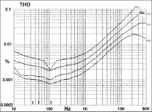
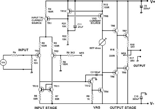
Figure 1 shows both the effects. The amplifier under test was a conventional Blameless design with an EF output stage comprising a single pair of sustained-beta bipolar power transistors; see Figure 2 for the basic circuit. Output power was 50 W into 8 Ω. The bottom trace is the distortion + noise with the usual source impedance of 50 Ω, and the top one shows how much worse the THD is with a source impedance of 3.9 K. Intermediate traces are for 2.2 K and 1.1 K sources. The THD residual shows both second harmonic distortion and 100 Hz ripple components, the latter dominating at low frequencies, while at higher ones the reverse is true. The presence of ripple is signalled by the dip in the top trace at 100 Hz, where distortion products and ripple have partially cancelled. The amount of degradation is proportional to the source impedance.
This is not a problem in most cases, where the preamplifier is driven by an active preamplifier, or by a buffer internal to the power amplifier. Competent preamplifiers have a low output impedance, often around 50–100 Ω, to minimise high-frequency losses in cable capacitance. (I have just been hearing of a system with 10 m of cable between preamp and power amp.)
However, there are two scenarios where the input source resistance is higher than this. If a so-called ‘passive preamp’ is used then the output impedance is both higher and volume-setting dependent. A 10 K volume potentiometer has a maximum output impedance of one-quarter the track resistance, i.e. 2.5 K, at its mid-point setting. It is also possible for significant source resistance to exist inside the power amplifier for example, there might be an balanced input amplifier, which while it has a very low output impedance itself, may have a resistive gain control network between it and the power amp.
So – we have a problem, or rather two of them. It seems very likely that the input transistor base currents are to blame for both, hence an obvious option is to minimise these currents by using transistors with the highest available beta in the input pair. In this amplifier the input pair were originally ZTX753, with a beta range of 70–200. Replacing these with BC556B input devices (beta range 180–460) gives Figure 3 which shows a useful improvement in THD above 1 kHz; distortion at 10 kHz drops from 0.04% to 0.01%. Our theory that the base currents are to blame is clearly correct. The bottom trace is the reference 50 Ω source plot with the original ZTX753s, and this demonstrates that the problem has been reduced but certainly not eliminated.

The amplifier here is very linear with a low source impedance, and it might well be questioned as to why the input currents drawn are distorted if the output is beautifully distortion-free. The reason is of course that global negative feedback constrains the output to be linear because this is where the NFB is taken from but the internal signals of the amplifier are whatever is required to keep the output linear. The VAS is known to be non-linear, so if the output is sinusoidal the collector currents of the input pair clearly are not. Even if they were, the beta of the input transistors is not constant so the base currents drawn by them would still be non-linear.
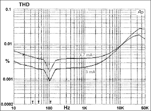
It is also possible to get a reduction in hum and distortion by reducing the input pair tail current, but this very important parameter also affects input stage linearity and the slew-rate of the whole amplifier. Figure 4 shows the result. The problem is reduced – though far from eliminated – but the high-frequency THD has actually got worse because of poorer linearity in the input stage. This is not a promising route to follow.
Both ripple and THD effects consequent on the base currents drawn could be eliminated by using FETs instead of bipolars in the input stage. The drawbacks are:
1. Poor Vgs matching, which means that a d.c. servo becomes essential to control the amplifier output d.c. offset. Dual FETs do exist but they are discouragingly expensive.
2. Low transconductance, which means the stage cannot be linearised by local feedback as the raw gain is just not available.
3. Although there is no d.c. gate current, there might well be problems with non-linear input capacitance, as there are with FET-input op-amps.
Once again, not a promising route.
The distortion problem looks rather intractable; one possible total cure is to put a unity-gain buffer between input and amplifier. The snag (for those seeking the highest possible performance) is that any opamp will compromise the noise and distortion of a Blameless amplifier. It is quite correct to argue that this doesn’t matter, as any preamp hooked up to the power amp will have opamps in it anyway, but the preamp is a different box, a different project, and possibly has a different designer, so philosophically this does not appeal to everyone. If a balanced input is required then an opamp stage is mandatory. (unless you prefer transformers, which of course have their own problems.)
The best choice for the opamp is either the commonplace but extremely capable 5532 (which is pretty much distortion-free, but not alas noise-free, though it is very quiet) or the rather expensive but very quiet AD797.
The ripple problem, however, has a more elegant solution. If there is ripple in the input base current, then clearly there is some ripple in the tail current. This is not normally detectable because the balanced nature of the input stage cancels it out. A significant input source impedance upsets this balance, and the ripple appears.
The tail is fed from constant-current source TR1, and this is clearly not a mathematically perfect circuit element. Investigation showed that the cause of the tail-current ripple contamination is Early effect in this transistor, which is effectively fed with a constant bias voltage A tapped off from the VAS negative-feedback current source. (Early effect is the modulation of transistor collector current caused by changing the Vce; as a relatively minor aspect of bipolar transistor behaviour it is modelled by SPICE simulators in a rather simplistic way.) Note that this kind of negative-feedback current-source could control the tail current instead of the VAS current, which might well reduce the ripple problem, but is arranged this way as it gives better positive slewing. Another option is two separate negative-feedback current-sources.
The root cause of our hum problem is therefore the modulation of the Vce of TR1 by ripple on the positive rail, and this variation is easily eliminated by cascoding, as shown in Figure 5. This forces TR1 emitter and collector to move up and down together, preventing Vce variations. It completely eradicates the ripple components, but leaves the input-current distortion unaltered, giving the results in Figure 6, where the upper trace is degraded only by the extra distortion introduced by a 2 K source impedance; the 100 Hz cancellation notch has also disappeared. The reference 50 Ω source plot is below it.
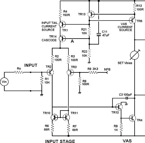

The voltage at A that determines the Vce of TR1 is not critical. It must be sufficiently below the positive supply rail for TR1 to have enough Vce to conduct properly, and it must be sufficiently above ground to give the input pair enough common-mode range. I usually split the biasing chain R21, R22 in half, as shown, so C11 can be used to filter out rail noise and ripple, and biasing the cascode transistor from the mid-point works very well.
It may have occurred to the reader that simply balancing the impedances seen by the two inputs will cancel out the unwanted noise and distortion. This is not very practical as with discrete transistors there is no guarantee that the two input devices will have the same beta. (I know there are such things as dual bipolars, but once more the cost is depressing.) This also implies that the feedback network will have to have its impedance raised to equal that at the input, which would give unnecessarily high levels of Johnson noise.
Conclusions
If the system design requires an opamp at the input, then both hum and distortion problems are removed with no further effort. If not, perhaps because the amplifier must be as quiet as possible, then cascoding the input pair tail cures the ripple problem but not the distortion. Using high-beta input transistors reduces both problems but does not eliminate them.