Trimodal audio power, Part I
This project had its roots in a large number of requests for a PCB for the Class-A amplifier described in the last part of the Distortion In Power Amplifiers series. Rather than just using the original circuit, I took the chance to look closely at output stage voltage efficiency, and also to re-examine the input stage balance and noise performance. I added a safety circuit to prevent catastrophe if the quiescent-current control arrangements went haywire, and this very conveniently doubles as the bias voltage generator when the amplifier is in the Class-B mode.
This proved a very popular design, and I had a lot of correspondence about it. People are still building them.
I present here my own contribution to global warming in the form of an improved Class-A amplifier that I believe is unique. It not only copes with load impedance dips by means of an unusually linear form of Class-AB, but will also operate as a ‘blameless’ Class-B engine. The power output in pure Class-A is 20 to 30 W into 8 Ω, depending on the exact supply rails chosen.
Initially, I simply intended to provide an updated version of the Class-A circuit published in reference 1, in response to requests for a PCB for the Class-A amplifier designed with my methodology. I decided to use a complementary-feedback-pair (CFP), output stage for best possible linearity, and some incremental improvements have been made to noise, slew rate and maximum d.c. offset.
Naturally, the Class-A circuit bears a very close resemblance to a ‘blame-less’ Class-B amplifier. As a result, I decided to retain the Class-B Vbe multiplier, and use it as a safety-circuit to prevent catastrophe if the relatively complex Class-A current-regulator failed. From this the idea arose of making the amplifier instantly switchable between Class-A/AB and Class-B modes. This gives two kinds of amplifier for the price of one, and permits of some interesting listening tests. Now you really can do an A/B comparison.
In the Class-B mode the amplifier has the usual negligible quiescent dissipation, but in Class-A the thermal efflux is naturally considerable. This is because true Class-A operation is extended down to 6 Ω resistive loads for the full output voltage swing, by suitable choice of the quiescent current.
With heavier loading the amplifier gracefully enters Class-AB, in which it will give full output down to 3 Ω before the safe-operating-area (SOAR), limiting begins to act. Output into 2 Ω is severely curtailed, as it must be with only one output pair, and this kind of load is not advisable.
In short, the amplifier allows a choice between being firstly very linear all the time – blameless Class-B – and secondly ultra-linear most of the time – Class-A – with occasional excursions into Class-AB.
The amplifier’s AB mode is still extremely linear by current standards, though inherently it can never be as good as properly-handled Class-B, and nothing like as good as A. Since there are three possible classes of operation I have decided to call the design a Trimodal power amplifier. It is impossible to be sure that you have read all the literature on an area of technology; however, to the best of my knowledge this is the first ever Trimodal amplifier.
As I said earlier, designing a low-distortion Class-A amplifier is in general a good deal simpler than the same exercise for Class-B. All the difficulties of arranging the best possible crossover between the output devices disappear. Because of this it is hard to define exactly what ‘blameless’ means for a Class-A amplifier.
In Class-B the situation is quite different, and ‘blameless’ has a very specific meaning; when each of the eight or more distortion mechanisms has been minimised in effect, there always remains the crossover distortion inherent in Class-B. There appears to be no way to reduce it without departing radically from that might be called the generic Lin amplifier configuration. Therefore the ‘blameless’ state appears to represent some sort of theoretical limit for Class-B, but not for Class-A.
However, Class-B considerations cannot be ignored, even in a design intended to be Class-A only, because if the amplifier does find itself driving a lower load impedance than expected, it will move into Class-AB. In this case, all the additional Class-B requirements are just as significant as for a Class-B design proper. Class-AB can never give distortion as low as optimally-biased Class-B, but it can be made comparable if the extra distortion mechanisms are correctly handled.
My correspondence has made it abundantly clear that EW readers are not going to be satisfied with anything less than state-of-the-art linearity, and so the amplifier described here uses the CFP type of output stage, which has the lowest distortion due to the local feedback loops enclosing the output devices. It also has the advantage of better output efficiency than the emitter-follower version, and inherently superior quiescent current stability. It will shortly be seen that these are both important for this design.
Half-serious thought was given to labelling the Class-A mode ‘distortion-less’ as the THD is completely unmeasurable across most of the audio band. However, detectable distortion products do exist above 10 kHz, so sadly, I abandoned this provocative idea.
Before putting cursor to CAD, it seemed appropriate to take another look at the Class-A design, to see if it could be inched a few steps nearer perfection. The result is a slight improvement in efficiency, and a 2 dB improvement in noise performance. In addition the expected range of output d.c. offset has been reduced from ± 50 mV to ± 15 mV, still without any adjustment.
The power and the glory
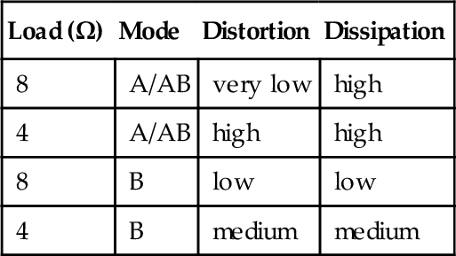
The amplifier is 4 Ω capable in both A/AB and B operating modes, though it is the nature of things that the distortion performance is not quite so good. All solid-state amplifiers – without qualification, as far as I am aware – are much happier with an 8 Ω load, both in terms of linearity and efficiency; loudspeaker designers please note.
With a 4 Ω load, Class-B operation gives better THD than Class-A/AB, because the latter will always be in AB mode, and therefore generating extra output stage distortion through gm -doubling. This should really be called gain-deficit-halving, but somehow I don’t see this term catching on. These not entirely obvious relationships are summarised on the right.
Figure 1 attempts to show diagrammatically just how power, load resistance, and operating mode are related. The rails have been set to ± 20 V, which just allows 20 W into 8 Ω in Class-A. The curves are lines of constant power, i.e. V × I in the load, the upper horizontal line represents maximum voltage output, allowing for Vce(sat)S, and the sloping line on the right is the SOAR protection locus; the output can never move outside this area in either mode. The intersection between the load resistance lines sloping up from the origin and the ultimate limits of voltage-clip and SOAR protection define which of the curved constant-power lines is reached.

In A/AB mode, the operating point must be left of the vertical push-pull current-limit line (at 3A, i.e. twice the quiescent current) for Class-A. If we move along one of the impedance lines, when we pass to the right of the push-pull limit the output devices will begin turning off for part of the cycle; this is the AB operation zone. In Class-B mode, the 3A line has no significance and the amplifier remains in optimal Class-B until clipping or SOAR limiting occurs. Note that the diagram axes represent instantaneous power in the load, but the curves show sine-wave r.m.s. power, and that is the reason for the apparent factor-of-two discrepancy between them.
Health and efficiency
Concern for efficiency in Class-A may seem paradoxical, but one way of looking at it is that Class-A watts are precious things, wrought in great heat and dissipation, and so for a given quiescent power it makes sense to ensure that the amplifier approaches its limited theoretical efficiency as closely as possible. I was confirmed in this course by reading of another recent design2 which seems to throw efficiency to the winds by using a hybrid bjt/FET cascode output stage. The voltage losses inherent in this arrangement demand ± 50 V rails and sixfold output devices for a 100 W Class-A capability; such rail voltages would give 156 W from a 100% efficient amplifier.
Voltage efficiency of a power amplifier is the fraction of the supply-rail voltage which can actually be delivered as peak-to-peak voltage swing into a specified load; efficiency is invariably less into 4 Ω due to the greater resistive voltage drops with increased current.
The Class-B amplifier I described in Ref. 3 has a voltage efficiency of 91.7% for positive swings, and 92.5% for negative, into 8 Ω. Amplifiers are not in general completely symmetrical, and so two figures need to be quoted; alternatively the lower of the two can be given as this defines the maximum undistorted sine-wave. These figures above are for an emitter-follower output stage, and a complementary-feedback pair output does better, the positive and negative efficiencies being 94.0% and 94.7% respectively.
The emitter follower version gives a lower output swing because it has two more Vbe drops in series to be accommodated between the supply rails; the CFP is always more voltage-efficient, and so selecting it over the emitter follower for the current Class-A design is the first step in maximising efficiency.
Figure 2 shows the basic complementary-feedback pair output stage, together with its two biasing elements. In Class-A the quiescent current is rigidly controlled by negative-feedback; this is possible because in Class-A the total voltage across both emitter resistors Re is constant throughout the cycle. In Class-B this is not the case, and we must rely on ‘thermal feedback’ from the output stage, though to be strictly accurate this is not ‘feedback’ at all, but a kind of feed-forward.
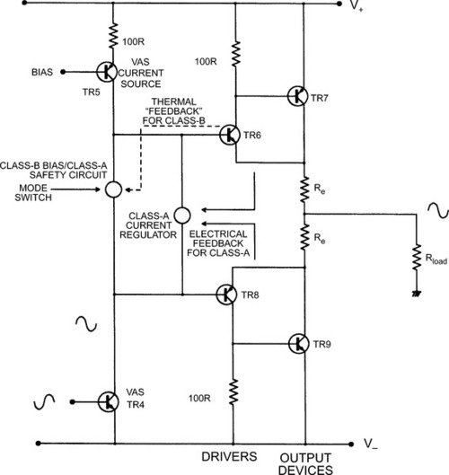
It is a big advantage of the CFP configuration that quiescent current, Iq depends only on driver temperature, and this is important in the Class-B mode, where true feedback control of quiescent current is not possible. This has special force if low-value emitter resistors such as 0.1 Ω, are chosen, rather than the more usual 0.22 Ω; the motivation for doing this will soon become clear.
Voltage efficiency for the quasi-complementary Class-A circuit of Ref. 1 into 8 Ω is 89.8% positive and 92.2% negative. Converting this to the CFP output stage increases this to 92.9% positive and 93.6% negative. Note that a Class-A Iq of 1.5 A is assumed throughout; this allows 31 W into 8 Ω in push-pull, if the supply rails are adequately high. However the assumption that loudspeaker impedance never drops below 8 Ω is distinctly doubtful, to put it mildly, and so as before this design allows for full Class-A output voltage swing into loads down to 6 Ω.
So how else can we improve efficiency? The addition of extra and higher supply rails for the small-signal section of the amplifier surprisingly does not give a significant increase in output; examination of Figure 3 shows why. In this region of operation, the output device Tr7 base is at a virtually constant 880 mV below the positive rail, and as Tr6 driver base rises it passes this level, and keeps going up; clipping has not yet occurred.
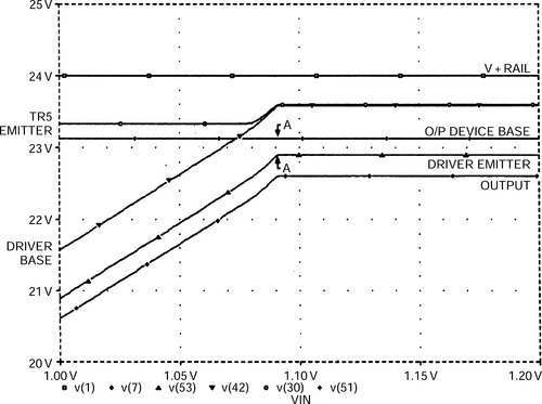
The driver emitter follows the driver base up, until the voltage difference between this emitter and the output base, i.e. the driver Vce, becomes too small to allow further conduction; this choke point is indicated by the arrows A-A. At this point the driver base is forced to level off, although it is still about 500 mV below the level of the positive rail. Note also how the voltage between the positive rail and Tr5 emitter collapses. Thus a higher rail will give no extra voltage swing, which I must admit came as something of a surprise. Higher sub-rails for small-signal sections only come into their own in FET amplifiers, where the high Vgs for FET conduction (5 V or more) makes their use almost mandatory.
Efficiency figures given so far are all greater for negative rather than positive voltage swings. The approach to the rail for negative clipping is slightly closer because there is no equivalent to the 0.6 V bias established across R13 ; however this advantage is absorbed by the need to lose a little voltage in the RC filtering of the negative supply to the current-mirror and voltage amplifier stage. This filtering is essential if really good ripple/hum performance is to be obtained3.
In the quest for efficiency, an obvious variable is the value of the output emitter resistors Re. The performance of the current-regulator described, especially when combined with a CFP output stage, is more than good enough to allow these resistors to be reduced while retaining first-class Iq stability. I took 0.1 Ω as the lowest practicable value, and even this is comparable with PCB track resistance, so some care in the exact details of physical layout is essential; in particular the emitter resistors must be treated as four-terminal components to exclude unwanted voltage drops in the tracks leading to the resistor pads.
If Re is reduced from 0.22 Ω to 0.1 Ω then voltage efficiency improves from 92.9%/93.6%, to 94.2%/95.0%. Is this improvement worth having? Well, the voltage-limited power output into 8 Ω is increased from 31.2 to 32.2 W with ± 24 V rails, at absolutely zero cost, but it would be idle to pretend that the resulting increase in sound-pressure level is highly significant. It does however provide the philosophical satisfaction faction that as much Class-A power as possible is being produced for a given dissipation; a delicate pleasure.
The linearity of the CFP output stage in Class-A is very slightly worse with 0.1 Ω emitter resistors, though the difference is small and only detectable open-loop; the simulated THD of an output stage alone (for 20 V pk-pk in 8 Ω) is only increased from 0.0027% to 0.0029%. This is probably due to simply to the slightly lower total resistance seen by the output stage.
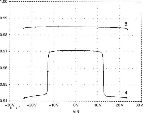
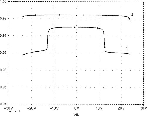
However, at the same time reducing the emitter resistors to 0.1 Ω provides much lower distortion when the amplifier runs out of Class-A; it halves the size of the step gain changes inherent in Class-AB, and so effectively reduces distortion into 4 Ω loads.
Figures 4 & 5 are output linearity simulations; the measured results from a real and ‘blameless’ Trimodal amplifier are shown in Figure 6, where it can be clearly seen that THD has been halved by this simple change. To the best of my knowledge this is a new result; my conclusion is that if you must work in Class-AB, keep the emitter resistors as low as possible, to minimise the gain changes.
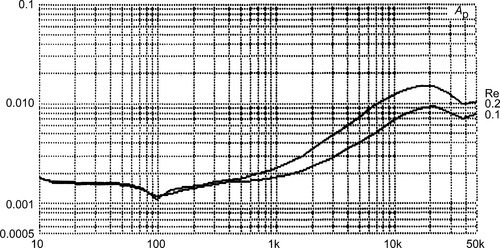
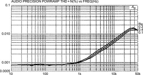
Having considered the linearity of Class-A and AB, we must not neglect what effect this radical Re change has on Class-B linearity. The answer is, not very much, but there is a slightly reduction in THD, Figure 7, where crossover distortion seems to be slightly higher with Re at 0.2 Ω than for either 0.1 or 0.4 Ω. Whether this is a consistent effect – for complementary-feedback pair stages anyway – remains to be seen.
The detailed mechanisms of bias control and mode-switching are described in the second part of this article.
Improving noise performance
In a power amplifier, noise performance is not an irrelevance.4 It is well worth examining just how good it can be. As in most amplifiers, noise is set here by a combination of the active devices at the input and the surrounding resistances.
Operating conditions of the input transistors themselves are set by the demands of linearity and slew-rate, and there is little freedom of design here; however the collector currents are already high enough to give nearoptimal noise figures with the low source impedances – a few hundred ohms – that we have here, so this is not too great a problem. Also remember that noise figure is a weak function of Ic, so minor tweaking makes no detectable difference. We certainly have the choice of input device type; there are many more possibilities now that we have relatively low rail voltages. Noise performance is, however, closely bound up with source impedance, and we need to define this before device selection.
Looking therefore to the passives, there are several resistances generating Johnson noise in the input, and the only way to reduce this noise is to reduce them in value. The obvious candidates are input stage degeneration resistors R2,3 and R9 , which determines the output impedance of the negative-feedback network. There is also another unseen component; the source resistance of the preamplifier or whatever upstream.
Even if this equipment were miraculously noise-free, its output resistance would still generate Johnson noise. If the preamplifier had, say, a 20 kΩ volume pot at its output – not a good idea, as this gives a poor gain structure and cable dependent h.f. losses, but that is another story5 – then the source resistance could be a maximum of 5 kΩ, which would almost certainly generate enough Johnson Noise to dominate the power-amplifier’s noise behaviour. However, there is nothing that power-amp designers can do about this, so we must content ourselves with minimising the noise-generating resistances we do have control over.
The presence of input degeneration resistors R2,3 is the price we pay for linearising the input stage by running it at a high current, and then bringing its transconductance down to a useable value by adding linearising local negative feedback. These resistors cannot be reduced, for if the h.f. negative-feed-back factor is then to remain constant, Cdom would have to be proportionally increaseed, with a consequent reduction in slew rate. Used with the original negative feedback network, these resistors degrade the noise performance by 1.7 dB. Like all the other noise measurements given here, this figure assumes a 50 Ω external source resistance.
If we cannot alter the input degeneration resistors, then the only course left is the reduction of the feedback network impedance, and this sets off a whole train of consequences. If R8 is reduced to 2.2kΩ, then R9 becomes 110 Ω, and this reduces noise output from − 93.5 dBu to − 95.4 dBu. Note that if R2,3 were not present, the respective figures would be − 95.2 and − 98.2 dBu. However, R1 must also be reduced to 2.2kΩ to maintain d.c. balance, and this is too low an input impedance for direct connection to the outside world.
If we accept that the basic amplifier will have a low input impedance, there are two ways to deal with it. The simplest is to decide that a balanced line input is essential; this puts an opamp stage before the amplifier proper, buffers the low input impedance, and can provide a fixed source impedance to allow the high and low-frequency bandwidths to be properly defined by an RC network using non-electrolytic capacitors. The common practice of slapping an RC network on an unbuffered amplifier input must be roundly condemned as the source impedance is unknown, and so therefore is the roll-off point. A major stumbling block for subjectivist reviewing, one would have thought.
The other approach is to have a low resistance d.c. path at the input but maintain a high a.c. impedance; in other words to use the fine old practice of input bootstrapping. Now this requires a low-impedance unity-gain-with-respect-to-input point to drive the bootstrap capacitor, and the only one available is at the amplifier inverting input, i.e. the base of Tr3. While this node has historically been used for the purpose of input bootstrapping6 it has only been done with simple circuitry employing very low feedback factors.
There is good reason to fear that any monkey business with the feedback point, at Tr3’s base, will add shunt capacitance, creating a feedback pole that will degrade h.f. stability. There is also the awkward question of what will happen if the input is left open-circuit.
Figure 8 shows how the input can be safely bootstrapped.
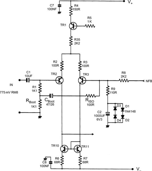
The total d.c. resistance of R1 and Rboot equals R8, and their centre point is driven by Cboot . Connecting Cboot directly to the feedback point did not produce gross instability, but it did seem to increase susceptibility to sporadic parasitic oscillation. Resistor Riso was added to isolate the feedback point from stray capacitance: this seemed to effect a complete cure.
The input could be left open-circuit without any apparent ill-effects, though this is not exactly good practice if loud-speakers are connected. A value for Riso of 220 Ω increases the input impedance to 7.5kΩ, and 100 Ω raises it to 13.3kΩ, safely above the 10 kΩ standard value for a bridging impedance. Despite successful tests, I must admit to a few lingering doubts about the high-frequency stability of this approach, and it might be as well to consider it as experimental until more experience is gained.
Another consequence of a low-impedance negative feedback network is the need for feedback capacitor C2 to be proportionally increased to maintain the low-frequency response, and prevent capacitor distortion from causing a rise in THD at low frequencies; it is the latter constraint that determines the value. This is a separate distortion mechanism from the seven previously considered, and I think deserves the title Distortion 8. This criterion gives a value of 1000 μF, which necessitates a low rated voltage such as 6.3 V if the component is to be of reasonable size. As a result, C2 now needs protective shunt diodes in both directions, because if the amplifier fails it may saturate in either direction.
Close examination of the distortion residual shows that the onset of conduction of back-to-back diodes will cause a minor increase in THD at 10 Hz, from less than 0.001% to 0.002%, even at the low power of 20 W/8 Ω. It is not my practice to tolerate such gross non-linearity, and therefore four diodes are used in the final circuit, and this eliminates the distortion effect, Figure 8. It could be argued that a possible reverse-bias of 1.2 V does not protect C2 very well, but at least there will be no explosion.
We can now consider alternative input devices to the MPSA56, which was never intended as a low-noise device. Several high-beta low-noise types such as 2SA970 give an improvement of about 1.8 dB with the low-impedance negative feedback network. Specialised low-Rb devices like 2SB737 give little further advantage – possibly 0.1 dB – and it is probably better to go for one of the high-beta types; the reason why will soon emerge.
It could be argued that the complications of a low-impedance negative feedback network are a high price to pay for a noise reduction of some 2 dB; however, there is a countervailing advantage, for the above negative feedback network modification significantly improves the output d.c. offset performance. The second and final part of this article shows how, and also gives full details of the mode-switching and bias control systems, and the performance of the complete amplifier.