
High-performance preamplifier
Low-cost design with active gain control
This was my first ‘conventional’ preamplifier design to be published. It was my own reaction to the relative complexity of the Advanced Preamplifier just described; I set out to produce a preamplifier that was conventional, to see just how good it could be. At that time the available op-amps were looked at with entirely justified suspicion; they were relatively noisy and prone to crossover distortion in their output stages. Crossover might be inescapable in a power amplifier, but it was definitely not a good thing to have in a preamp. Hence the use of discrete Class-A circuitry throughout. (The 5534 op-amp was just becoming available at the time, but was ferociously expensive.)
The basic philosophy was the use of simple two or three-transistor stages, enhanced with current-source outputs when required, running from a rather high rail voltage to increase head-room and reduce distortion at a given signal level. A single supply rail was used, without regulation, but with an extra RC filter to reduce ripple to about 50 mV. This minimal-cost arrangement gave hum and noise figures as good as those from the dual-rail, IC regulator method. Where it fell down was that there was of course no DC regulation, so when the rather low noise and distortion were being measured, the audio analyser residual signal heaved up and down like a rough sea, making measurements rather tricky, even when a high-pass filter was employed.
Note the transistor equivalent of the White cathode-follower at the disc-stage output, giving push-pull Class-A operation with beautiful simplicity. Not so conventional after all.
Some years ago Doug Self described a no-compromise preamplifier which was designed using high voltage transistors to give exceptional performance. This new design sacrifices very little of that performance and uses a small number of low-cost transistors to significantly reduce the cost. A novel active gain control makes best use of the dynamic range and removes the problem of volume control placement.
This preamplifier offers a similar performance to that of the advanced preamplifier published previously,1 but with a simpler design that reduces the parts count and hence cost. In normal use, the signal levels are kept around 50 mV by exchanging the normal potentiometer volume control, which acts as an attenuation control, for an active gain control. Therefore, the signal receives only the amplification required for a given output and so makes best use of the amplifier’s dynamic range.
The distortion performance is also improved because unwanted gain will be used to give higher negative feedback and thus greater linearity. The active gain control uses a shunt feedback circuit where the volume control varies the resistance of a feedback arm as shown in Figure 1. The disc input stage has a relatively low gain of + 20 dB at 1 kHz which allows a very high input overload margin. This is followed by a third-order high-pass filter which removes subsonic signals while they are still at a low level. Both bass boost and treble cut portions of the RIAA equalisation take place in the first stage. The gain control stage is positioned after the input switching and has a maximum voltage gain of + 20 dB. This is followed by a Baxandall tone control which has unity gain at 1 kHz.
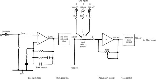
The use of an active gain control eliminates the problems associated with a normal volume control. If all of the gain is placed before the control, the supply voltage limits the overload margin. If some gain occurs after the volume control, then the signal-to-noise ratio is degraded because noise generated in the later stages does not undergo attenuation. The use of two controls, one early and one late in the signal chain, is one method of avoiding this compromise1 but a true gain control is considered to be a more elegant solution.
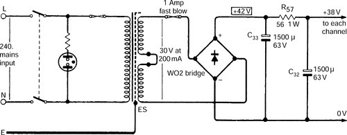
Because a low-cost, single unregulated power supply is used with first-order RC smoothing to reduce ripple, all sections of the preamplifier are designed with high ripple-rejection performance.
Disc input stage
The most difficult stage to design in a preamplifier is the disc input, and the problems are compounded if, as in this case, the gain of the stage is low to allow a high overload margin. A low voltage gain at 1 kHz means that the feedback network which defines the gain and RIAA equalisation will have a relatively low impedance, and thus appear as a heavy load to be driven by the disc amplifier. This situation becomes worse at higher frequencies when the reactance of the equalisation components falls. Therefore, as a large voltage swing at the output is desirable, a large amount of current must be able to flow into and out of the feedback network at high frequencies. A second, and related problem, is that if the gain at 1 kHz is low, the gain at 20 kHz must be 19.3 dB lower due to the RIAA equalisation, which makes it close to unity. Therefore, it becomes more difficult to set the top end of the RIAA curve accurately. For this reason an extra low-pass section, with a − 3 dB frequency of about 22 kHz, is added after the disc amplifier to ensure that the high-frequency gain continues to fall at a steady rate. It should be noted that if the correct turn-over frequency is chosen for the final low-pass network, the RIAA amplitude and phase curves are obtained ex
Another consequence of the fall in closed-loop gain at high frequencies is that the compensation for Nyquist stability is more difficult, and in this design it was necessary to add a conventional RC step-network to the normal dominant-pole compensation. The dominant-pole capacitor is kept as small as possible to preserve the slew-rate capability of the stage.
The basic disc input stage is shown in Figure 2. In this series-feedback configuration almost all of the voltage gain is provided by the second transistor, which has a bootstrapped collector load for high open-loop gain and linearity. The final transistor is an emitter-follower for unity-gain voltage buffering. This configuration allows the use of a p-n-p input transistor for optimum noise performance, but it also means that the collector current must flow through the feedback resistance RF. This places another constraint on the design of the feedback network because an excessive voltage drop must be avoided.
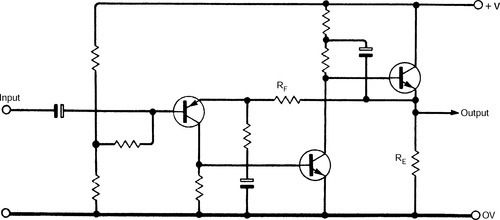
As the disc input amplifier must be capable of sourcing or sinking large peak values of current to drive the capacitive feedback loop at high frequencies, the conventional emitter-following output circuit in Figure 2 is not suitable because the sink current causes a voltage drop in RE. Lowering the value of RE reduces the effect, but this is a poor solution as it leads to a high quiescent power dissipation. Replacing RE with a constant-current source is more effective because the maximum sink current becomes equal to the standing current of the stage. However, this would still limit the output of the disc stage at high audio frequencies due to an inability to sink sufficient current. For this reason, the push-pull class A configuration in Figure 3 was chosen. The bottom transistor is a current-source which is modulated in anti-phase to the top emitter-follower, via the current-sensing resistor RA and a capacitor. This can also be considered as a negative-feedback loop that attempts to keep the current in RA constant. However, the open-loop gain is only unity and so with 100% negative feedback the current variations in the top transistor are reduced to one half by the capacitor. Due to the anti-phase drive of the lower transistor, this stage can sink a peak current of twice the standing current, and therefore give twice the output swing at high frequencies.

A practical circuit of the disc input amplifier and its associated subsonic filter is shown in Figure 4. All of the d.c. bias voltages are provided by the potential divider R2, R3, R4, D1 and D2. This chain is heavily decoupled by C2 to prevent supply-rail ripple entering this sensitive part of the circuit. Note that Tr3 and Tr5 are isolated from the bias voltage by R14 and R22 to simplify any fault-finding.
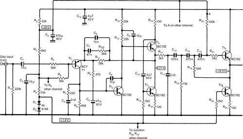

The RIAA equalisation is provided by R10, R11, C6 and C7 in the feedback loop, and R7, C4 forms a step network that aids h.f. stability. Resistor R17 and C11 make up the low-pass section that corrects the top octave of the RIAA curve. The subsonic filter is a 3-pole Butterworth type with an ultimate slope of 18 dB/octave. Although the frequency response shows a loss of only 1.5 dB at 20 Hz, the attenuation is increased to more than 14 dB at 10 Hz. The unity-voltage gain element of the filter is formed by Tr5 and Tr6 arranged as an emitter-follower with a current-source load. This configuration was chosen for its excellent linearity. An output of about 50 mV is available for tape recording although the exact voltage will depend on the cartridge sensitivity. Resistor R24 prevents damage to Tr6 if the tape output is shorted to earth, and resistor R25 maintains the output of the disc stage at 0 V d.c., and also prevents switching clicks.
The total harmonic distortion from input to tape output at 6 V r.m.s. is below 0.004% from 1 to 10 kHz but because the anticipated signal level here from most cartridges is about 50 mV r.m.s. The distortion during use will be even lower. The disc input will accept more than 1 V r.m.s. at 1 kHz, and about 3.8 V r.m.s. at 10 kHz before overloading. It is felt that the improvement these figures show over conventional methods justifies the complication of a low-gain disc input stage. The accuracy of the RIAA equalisation depends on how closely the RC time-constants can be set. If 5% components are used the deviation should be less than ± 0.5 dB from 1 to 15 kHz, and within ± 1 dB from 20 Hz to 20 kHz. The signal-to-noise ratio for a 5 mV r.m.s. input at 1 kHz is better than 68 dB.
The remaining part of the preamplifier comprises an active gain-control and the tone-control stage. The input switching is simple and requires only one switch section per channel. Also, any line input of suitable sensitivity can be used as a tape monitor return.
The shunt-feedback configuration of the active gain control enables each line input to have its sensitivity defined by the value of a single series input resistor. The maximum voltage gain available from the stage is the ratio of the feedback resistance to the input resistance, and is + 20 dB when the volume control is at maximum resistance. This gain is only used in the disc mode. The most sensitive line input is rated at 100 mV for a 500 mV output and the least sensitive input has unity gain. Any sensitivity between these two limits may be provided by using the appropriate series resistor value.
The gain control comprises Tr7 and Tr8 arranged as a cascode voltage amplifier with a bootstrapped collector load and Tr9 as a conventional emitter-follower. The d.c. conditions are set by negative feedback through R37 and R38, and a.c. feedback is applied through the volume control. The linearity of this circuit is increased by a current injected into Tr7 through R33. The voltage at the top of R33 and the potential divider R30, R31, is smoothed by R32 and C17. Resistor R40 prevents high-frequency instability when the volume control is set to zero gain.
The tone-control is a conventional Baxandall circuit, with Tr10 providing a high voltage-gain by its bootstrapped collector load. Transistor Tr11 is another emitter-follower which buffers the high impedance at the collector of Tr10. The output is taken through R52, which protects the output against short-circuits. Because the output impedance is low, long cables may be used without loss of high frequencies. The power supply is shown in Figure 5.
Construction
Normal precautions should be taken to keep a.c. power away from the disc input stage, and to avoid earth loops. The leads to R54 should be kept short to prevent hum pick-up on the virtual-earth point of the gain control. Typical voltages for various parts of the circuit are shown in Figure 4. These measurements should be made with a 20 kΩ/V meter.
Several modifications can be made to the preamplifier to suit individual requirements. Firstly, the treble turnover frequency of the tone-control section can be increased from 2 kHz as shown in Figure 4, to 5 kHz, for example, by reducing C25 to 1000 pF. For variable turnover frequencies C25 can be made switchable. Some purists may feel that the provision of a tone-control is unnecessary, and even undesirable. In this case, the output should be taken from the junction of C22 and R54, but R52 and R53 should be retained at the output. Because the current drawn by the preamplifier will now be less, it is advisable to raise the value of R57 to keep the supply rail at + 38 V.
In the circuit of Figure 4, no balance control is included. This function was performed in the prototype by a dual-concentric volume control. If, however, a conventional balance network is required this can be added at the output of the preamplifier although the low output impedance will be sacrificed.