
Chapter 7. The Physical Basis of Transmission Lines
We hear the words transmission line all the time and we probably use them ever day, yet what really is a transmission line? A coax cable is a transmission line. A PCB trace in a multilayer board is a transmission line.
Tip
Fundamentally, a transmission line is composed of any two conductors that have length. This is all it takes to make a transmission line.
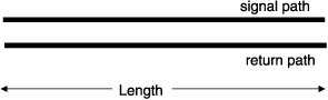
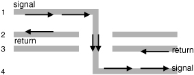
As we will see, a transmission line is used to transport a signal from one point to another. Figure 7-1 illustrates the general features of all transmission lines. To distinguish the two conductors, we refer to one as the signal path and the other as the return path.
Figure 7-1 A transmission line is any two conductors with length. We label one of the conductors as the signal path, the other as the return path.
A transmission line is a new ideal circuit element with very different properties of the three previously introduced ideal circuit elements: resistors, capacitors, and inductors. It has two very important parameters: a characteristic impedance and a time delay. The way a signal interacts with an ideal transmission line is radically different from the way it interacts with the other three ideal elements.
Though in some cases we can approximate the electrical properties of an ideal transmission line with combinations of L’s and C’s, the behavior of an ideal transmission line matches the actual, measured behavior of real interconnects much better and to much higher bandwidth than does an LC approximation. Adding an ideal transmission line circuit element to our toolbox will dramatically increase our ability to describe the interactions of signals and interconnects.
7.1 Forget the Word Ground
Too often, the other line in a transmission line is referred to as the ground line.
Tip
Far more problems are created than solved by referring to the second line as the ground. It is a good habit to use the term return path instead.
One of the most common ways of getting in trouble with signal-integrity design is overusing the term ground. It is much healthier to get in the habit of calling the other conductor and thinking about it as the return path.
Many of the problems related to signal integrity are due to poorly designed return paths. If we are always consciously aware that the other path plays the important role of being the return path for the signal current, we will take as much care in designing its geometry as we take for the signal path.
When we label the other path as ground, we typically think it is a universal sink for current. Return current goes into this connection and comes out wherever there is another ground connection. This is totally wrong. The return current will closely follow the signal current. As we saw in the last chapter, at higher frequencies, the loop inductance of the signal and return paths will be minimized, which means the return path will distribute as close to the signal path as the conductors will allow.
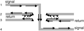
Further, the return current has no idea what the absolute voltage level is of the return conductor. The actual return conductor may in fact be a voltage plane such as the Vcc or Vdd plane. Other times, it might be a low-voltage plane. That it is labeled as a ground connection in the schematic is totally irrelevant to the signal, which is propagating on the transmission line. Start calling the return path the return path and problems will be reduced in the future. This guideline is illustrated in Figure 7-2.
Figure 7-2 Forget the word ground and more problems will be avoided than created.

7.2 The Signal
As we will see, when a signal moves down a transmission line, it simultaneously uses the signal and the return path. Both conductors are equally important in determining how the signal interacts with the interconnect.
When both lines look the same, as in a twisted pair, it is inconsequential which we call the signal path and which we call the return path. When one is different from the other, such as in a microstrip, we usually refer to the narrow conductor as the signal path and the plane as the return path.
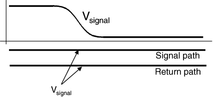
When a signal is launched into a transmission line, it will propagate down the line at the speed of light in the material. After the signal is launched in the transmission line, we can freeze time a moment later, move along the line, and measure the signal. The signal is always the voltage difference between two adjacent points on the signal and return paths. This is illustrated in Figure 7-3.
Figure 7-3 Map of the signal, frozen in time on a transmission line. The signal is the voltage between two adjacent points on the signal and the return paths.
Tip
If we know the impedance the signal sees, we can always calculate the current associated with the signal voltage. In this respect, a signal is equally well defined as a voltage or a current.
These general principles apply to all transmission lines, single ended, and as we will see, differential transmission lines.
7.3 Uniform Transmission Lines
We classify transmission lines by their geometry. The two general features of geometry that strongly determine the electrical properties of a transmission line are how uniform the cross section is down its length and how identical each of its two conductors is.
When the cross section is the same down the length, as in a coax cable, the transmission line is called uniform. Examples of various uniform transmission lines are illustrated in Figure 7-4.
Figure 7-4 Examples of cross sections of uniform transmission lines commonly used as interconnects.
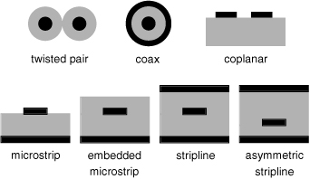
As we will see, uniform transmission lines are also called controlled impedance lines. There are a great variety of uniform transmission lines, such as twin leads, microstrips, striplines, and coplanar lines.
Tip
Reflections will be minimized and signal quality optimized, if the transmission lines are uniform, or have controlled impedance. All high-speed interconnects should be designed as uniform transmission lines.
Nonuniform transmission lines exist when some geometry or material property changes as we move down the length of the line. For example, if the spacing between two wires is not controlled but varies, this is a nonuniform line. A pair of leads in a dual in-line package (DIP) or quad flat pack (QFP) are nonuniform lines. Adjacent traces in a connector are often nonuniform transmission lines. Traces on a PCB that do not have a return-path plane are often nonuniform lines. Nonuniform transmission lines will lead to signal-integrity problems and should be avoided, unless they are kept short enough.
Tip
One of the goals in designing for optimized signal integrity is to design all interconnects as uniform transmission lines and to minimize the length of all nonuniform transmission lines.
Another quality of the geometry affecting transmission lines is how similar the two conductors are. When each conductor is the same shape and size as the other one, there is symmetry and we call this line a balanced line. A pair of twisted wires is symmetric since each conductor looks identical. A coplanar line has two narrow strips side by side on the same layer and is balanced.
A coax cable is unbalanced since the center conductor is much smaller than the outer conductor. A microstrip is unbalanced, since one wire is a narrow trace while the second is a wide trace. A stripline is unbalanced for the same reason.
Tip
In general, for most transmission lines, the signal quality and cross-talk effects will be completely unaffected by whether the line is balanced or unbalanced. However, ground-bounce and EMI issues will be strongly affected by the specific geometry of the return path.
Whether the transmission line is uniform or nonuniform, balanced or unbalanced, it has just one role to play: to transmit a signal from one end to the other with an acceptable level of distortion.
7.4 The Speed of Electrons in Copper
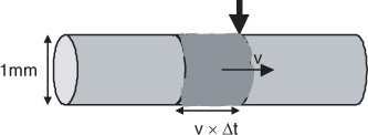
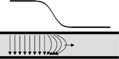
How fast do signals travel down a transmission line? If is often erroneously believed that the speed of a signal down a transmission line depends on the speed of the electrons in the wire. With this false intuition, we might imagine that lowering the resistance of the interconnect will increase the speed of a signal. In fact, the speed of the electrons in a typical copper wire is actually about 10-billion-times slower than the speed of the signal.
It is easy to estimate the speed of an electron in a copper wire. Suppose we have a roughly 18-gauge round wire, 1 mm in diameter, with 1 Amp of current. We can calculate the speed of the electrons in the wire based on how many electrons pass by one section of the wire per second, the density of the electrons in the wire, and the cross-sectional area of the wire. This is illustrated in Figure 7-5. The current in the wire is related to:
![]()
from which we can calculate the velocity of the electrons as:
![]()
where:
I = the current passing one point, in Amps
ΔQ = the charge flowing in a time interval, in Coulombs
Δt = the time interval
q = the charge of one electron, = 1.6 × 10⁻¹⁹ Coulombs
n = the density of free electrons, in #/m3
A = the cross-sectional area of the wire, in m2
v = the speed of the electrons in the wire, in m/sec
Figure 7-5 The electrons moving down a wire. The number passing the arrow per second is the current and is related to their velocity and number density.
Each copper atom contributes roughly two free electrons that can move through the wire. Atoms of copper are about 1 nm apart. This makes the density of free electrons, n, about n ~ 1027/m3.
For a wire that is 1 mm in diameter, the cross-sectional area is about A ~ 10−6 m2. Combining these terms and using a 1-Amp current in the wire, the speed of an electron in the wire can be estimated to be roughly:
![]()
Tip
An electron travels at a speed of about 1 cm/sec. This is about as fast as an ant scurries on the ground.
With this simple analysis, we see that the speed of an electron in a wire is incredibly slow compared to the speed of light in air. The speed of an electron in a wire really has virtually nothing to do with the speed of a signal. Likewise, as we will see, the resistance of the wire has only a very small, almost irrelevant effect on the speed of a signal in a transmission line. It is only in extreme cases that the resistance of an interconnect affects the signal speed, and then only very slightly. We must recalibrate our intuition from the erroneous notion that lower resistance will mean faster signals.
7.5 The Speed of a Signal in a Transmission Line
If it’s not the speed of the electrons that determines the speed of the signal, what does?
Tip
The speed of a signal depends on the materials that surround the conductors and how quickly the changing electric and magnetic fields associated with the signal can build up and propagate in the space around the transmission line conductors.
The simplest way to think of a signal propagating down a transmission line is illustrated in Figure 7-6. The signal, after all, is a voltage difference between the signal path and the return path. As the signal propagates, a voltage difference must be created between the two conductors. Accompanying the voltage difference is an electric field between the conductors.
Figure 7-6 The electric field building up in a transmission line as the signal propagates down the line. The speed of the signal depends on how fast the changing electric and magnetic fields can build up and propagate in the materials surrounding the signal- and return-path conductors.
In addition to the voltage, a current must be flowing in the signal conductor, and in the return conductor, to provide the charge that charges up the conductors that generates the voltage difference that creates the electric field. This current loop moving through the conductors will produce a magnetic field.
A signal can be launched into a transmission line simply by touching the leads of a battery to the signal and return paths. The sudden voltage change creates a sudden electric and magnetic-field change. This kink of field will propagate through the dielectric material surrounding the transmission line at the speed of a changing electric and magnetic field, which is the speed of light in the material.
We usually think of light as the electromagnetic radiation we can see. However, all changing electromagnetic fields are exactly the same and are described by exactly the same set of equations, Maxwell’s Equations. The only difference is the frequency of the waves. For visible light, the frequency is about 1,000,000 GHz. For the signals typically found in high-speed digital products, the frequency is about 1–10 GHz.
How quickly the electric and magnetic fields can build up is what really determines the speed of the signal. The propagation and interaction of these fields is described by Maxwell’s Equations. These say that if the electric and magnetic fields ever change, the kink they make will propagate outward at a speed that depends on some constants and material properties.
The speed of the change, or the kink, v, is given by:
![]()
where:
ε0 = permittivity of free space = 8.89 × 10⁻¹² F/m
εr = relative dielectric constant of the material
μ0 = permeability of free space = 4π × 10−7 H/m
μr = relative permeability of the material
Putting in the numbers, we find,
Tip
In air, where the relative dielectric constant and relative permeability are both 1, the speed of light is about 12 inches/nsec. This is a really good rule of thumb to keep in mind.
For virtually all interconnect materials, the magnetic permeability of the dielectrics, μr, is 1. All polymers that do not contain a ferromagnetic material have a magnetic permeability of 1. Therefore, this term can be ignored.
In comparison, the relative dielectric constant of materials, εr, is never less than or equal to 1, except for in the case of air. In all real interconnect materials, the dielectric constant is greater than 1. This means the speed of light in interconnects will always be less than 12 inches/nsec. The speed is:
![]()
For brevity, we usually refer to the relative dielectric constant as just the “dielectric constant.” This number characterizes some of the electrical properties of an insulator. It is an important electrical property. For most polymers, it is roughly 4. For glass, it is about 6 and for ceramics, it is about 10.
It is possible in some materials for the dielectric constant to vary with frequency. In other words, the speed of light in a material may be frequency dependent. In general, the dielectric constant decreases with higher frequency. This makes the speed of light in the material increase as we go toward higher frequency.
In most common materials, such as FR4, the dielectric constant varies very little from 500 MHz to 10 GHz. Depending on the ratio of epoxy resin to fiber glass, the dielectric constant of FR4 can be from 3.5 to 4.5. Most interconnect laminate materials have a dielectric constant of about 4. This suggests a simple, easy-to-remember generalization.
Tip
A good rule of thumb to remember is that the speed of light in most interconnects is about 12 inches/nsec / sqrt(4) = 6 inches/nsec. When evaluating the speed of signals in a boardlevel interconnect, we can assume they are about 6 inches/nsec.
As pointed out in an earlier chapter, when the field lines see a combination of dielectric materials, as in a microstrip where there are some field lines in the bulk material and some in the air above, the effective dielectric constant that affects the signal speed is a combination of the different materials. The only way to predict the effective dielectric constant when the materials are inhomogeneous throughout the cross section is with a 2D field solver. In the case of stripline, for example, all the fields see the same material and the effective dielectric constant is the bulk dielectric constant.
The time delay, TD, and length of an interconnect are related by:
![]()
where:
TD = the time delay, in nsec
Len = the interconnect length, in inches
v = the speed of the signal, in inches/nsec
This means that to travel down a 6-inch length of interconnect in FR4, for example, the time delay is about 6 inches / 6 inches/nsec or about 1 nsec. To travel 12 inches takes about 2 nsec.
The wiring delay, the number of psec of delay per inch of interconnect, is also a useful metric. It is just the inverse of the velocity: 1/v. For FR4, the wiring delay is about 1/6 inches/nsec = 0.166 nsec/inch, or 170 psec/inch. This is the delay of a signal propagating down a transmission line in FR4. Every inch of interconnect has a propagation delay of 170 psec. The wiring delay through the 0.5 inch of a BGA lead is 170 psec/inch × 0.5 inches = 85 psec.
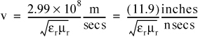
7.6 Spatial Extent of the Leading Edge
Every signal has a rise time, RT, usually measured from the 10% to 90% voltage levels. As a signal moves down a transmission line, the leading edge spreads out on the transmission line and has a spatial extent. If we could freeze time and look at the size of the voltage distribution as it moves out, we would find something like Figure 7-7.
Figure 7-7 Spatial extent of the leading edge of the signal as it propagates down a transmission line.
The length of the rise time, d, on the transmission line depends on the speed of the signal and the rise time:
![]()
d = the spatial extent of the rise time, in inches
RT = the rise time of the signal, in nsec
v = the speed of the signal, in inches/nsec
For example, if the speed is 6 inches/nsec and the rise time is 1 nsec, the spatial extent of the leading edge is 1 nsec × 6 inches/nsec = 6 inches. As the leading edge moves down the circuit board, it is really a 6-inch section of rising voltage moving down the board. A rise time of 0.1 nsec has a spatial extent of 0.6 inch.
Tip
Many of the signal-integrity problems related to imperfections in the transmission line depend on the size of the discontinuity compared to the spatial extent of the leading edge. It is always a good idea to be aware of the spatial extent of the leading edge for all signals.
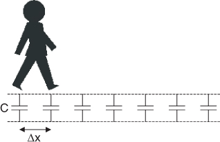
7.7 “Be the Signal”
All a signal cares about is how fast it moves down the line and what impedance it sees. As we saw previously, speed is based on the material properties of the dielectric and their distribution. To evaluate the impedance a signal sees in propagating down the line, we will take a microstrip transmission line and launch a signal into one end. A microstrip is a uniform, but unbalanced transmission line. It has a narrow-width signal line and a wide return path.
The analysis we will do of this line is identical to that for any transmission line. We’ll make it 10 feet long, so that we can actually walk down it and, in a Zen way, “be the signal” to observe what the signal would see. With each step along the way we will ask, what impedance do we see? We will answer this question by determining the ratio of the voltage applied, 1 v, and the current coming out of our foot to drive the signal down the transmission line.
In this case, we launch a signal into one end by connecting a 1-v battery between the two conductors at the front end. At the initial instant we have launched the signal into the line, there has not been enough time for the signal to travel very far down the line.
Just to make it easier, let’s assume that we have air between the signal and return paths, so the speed of propagation is 1 foot per nsec. After the first nsec, the voltage on the far end of the line is still zero, as the signal hasn’t had enough time to get very far. The signal along the line would be about 1 volt for the first foot and zero for the remaining length of the line.
Let’s freeze time after the first nsec and look at the charges on the line. What we see is illustrated in Figure 7-8. Between the signal- and return-path conductors in the first 12 inches, there will be a 1-volt difference. This is, after all, the signal. We know that because the signal and return paths are two separated conductors, there will be some capacitance between the conductors in this region. If there is a 1-v difference between them, there must also be some charge on the signal conductor and an equal and opposite amount on the return-path conductor.
Figure 7-8 Charge distribution on the transmission line after a 1-v signal has propagated for 1 nsec. There is no charge ahead of us (the signal) at this instant of time.
In the next 1 nsec, we, being the signal, will move ahead another 12 inches. Let’s stop time again. We now have the first two feet of line charged up. We see that having made this last step, we have brought the signal to the second foot-long section and created a voltage difference between the signal and return conductors. There is now a charge difference between the two conductors, at the point of each footstep, where there was none a nsec ago.
As we walk down the line, we are bringing a voltage difference to the two conductors and charging them up. In each nsec, we take another 1-foot step and charge up this new section of the line. Each step of the signal will leave another foot of charged transmission line in our wake.
The charge that flowed to charge up each footstep came from the signal as each foot came down and ultimately from the battery. The fact that the signal is propagating down the line means that the capacitance between the signal and return paths is getting charged up. How much charge has to flow from our foot into the line, in each footstep? In other words, what is the current that must flow as the signal propagates?
If the signal is moving down the line at a steady speed and the line is uniform, that is, it has the same capacitance per foot of length, then we are injecting the same amount of charge into the line with each footstep. Each step charges up the same amount of capacitance to the same voltage. If we are always taking the same time per step, then there is the same charge per unit of time required for the signal to charge up the line. The same amount of charge per nsec flowing into the line means that there is a constant current flowing into the line from our foot.
Tip
From the signal’s perspective, as we walk down the line at our speed of 1 foot/nsec, we are charging up each foot of line in the same amount of time. Coming out of the bottom of our foot is the charge that is added to the line to charge it up. An equal charge out of our foot in an equal time interval means we are injecting a constant current into the line.
What affects the current coming out of our foot to charge up the line? If we are moving down the line at a constant speed, and if we were to increase the width of the signal path, the capacitance we need to charge up will increase and the charge that must come out of our foot in the time we have till the next step will also increase. Likewise, if anything is done to decrease the capacitance per length, the current coming out of our foot will decrease. For the same reason, if the capacitance per length stays the same, but our speed increases, we will be charging up more length per nsec and the current needed will increase.
In this way, we can deduce that the current coming out of our foot will scale directly with both the capacitance per length and the speed of the signal. If either increases, the current out of our foot with each step will increase. If either decreases, the current from the signal to charge up the line will decrease. We have deduced a simple relationship between the current coming out of our foot and the properties of the line:
![]()
I = the current out of our foot
v = the speed with which we move down the line, charging up regions
CL = the capacitance per length of the line
As we, the signal, move down the transmission line, we will constantly be asking, “what is the impedance of the line?” The basic definition of impedance of any element is the ratio of voltage applied to current through it. So as we move down the line, we will constantly be asking with each footstep, what is the ratio of the voltage applied to the current being injected into the line?
The voltage of the signal is fixed at the signal voltage. The current into the line depends on the capacitance of each footstep and how long it takes to charge up each one. As long as the speed of the signal is constant and the capacitance of each footstep is constant, the current injected into the line by our foot will be constant and the impedance of the line the signal sees will be constant.
Suppose the line width were to suddenly widen. The capacitance of each footstep would be larger and the current coming out of each footstep to charge up this capacitance would be larger. A higher current for the same voltage means we see the transmission line having a lower impedance. Likewise, if the line were to suddenly narrow, the capacitance of each footstep would be less, the current required to charge it up would be less, and the impedance the signal would see for the line would be higher.
Tip
We call the impedance the signal sees with each step, the instantaneous impedance of the transmission line. As the signal propagates down the line, it is constantly probing the instantaneous impedance of each footstep, as the ratio of the voltage applied to the current required to charge the line and propagate toward the next step.
The instantaneous impedance depends on the speed of the signal, which is a material property, and the capacitance per length. For a uniform transmission line, the cross-sectional geometry is constant down the line and the instantaneous impedance the signal sees will be constant down the line. As we will see, an important behavior of a signal interacting with a transmission line is that whenever the signal sees a change in the instantaneous impedance some of the signal will reflect and some will continue distorted. Additionally, signal integrity may be affected. This is the primary reason why controlling the instantaneous impedance the signal sees is so important.
Tip
The chief way of minimizing reflection problems is to keep the instantaneous impedance the signal sees constant by keeping the geometry constant. This is what is meant by a controlled-impedance interconnect, or a constant instantaneous impedance down the length.
7.8 The Instantaneous Impedance of a Transmission Line
We can quantify this analysis by building a simple physical model of the transmission line. We have modeled the line as an array of little capacitor buckets, each one equal to the capacitance in the transmission line that spans a footstep and separated by the distance we, the signal, move in each footstep. We call this model (the simplest model we can come up with that provides engineering insight) the zeroth-order model of a transmission line. It is a physics model and not an equivalent circuit model. Circuit models do not have lengths in them. This model is outlined in Figure 7-9.
Figure 7-9 Zeroth-order model of a transmission line composed of an array of capacitors. With each footstep another capacitor is charged up. The spacing is the size of our footstep.
In this model, the size of each footstep is Δx. The magnitude of each little capacitor bucket is the capacitance per length, CL, of the line times the length of each footstep:
![]()
We can calculate the current out of our foot, I, using this model. The current is the charge that flows out of our foot to charge up each bucket in the time interval between each step. The charge we dump in each capacitor bucket, Q, is the capacitance of the bucket times the voltage applied, V. For each step we take, we are dumping the charge Q into the line, in a time interval of a step. The time between steps, Δt, is the length of our step, Δx, divided by our speed down the line, v. Of course, as the real signal propagates, each footstep is really small, but the time interval gets really small as well. The ratio of the charge required to each time interval is a constant value, which is the current that flows into the line as the signal propagates:
where:
I = the current from the signal
Q = the charge in each footstep
C = the capacitance of each footstep
Δt = the time to step from capacitor to capacitor
CL = the capacitance per length of the transmission line
Δx = the distance between the capacitors or each footstep
v = the speed of walking down the line
V = the voltage of the signal
This says the current coming out of our foot and going into the line is simply related to the capacitance per length, the speed of propagation, and the voltage of the signal—exactly as we reasoned.
This is the defining relationship for the current-voltage (I-V) behavior of a transmission line. It says the instantaneous current of a signal everywhere on a transmission line is directly proportional to the voltage. Double the voltage applied and the current into the transmission line will double. This is exactly how a resistor behaves. With each step down the transmission line, the signal sees an impedance that behaves like a resistive load.
From this relationship, we can calculate the instantaneous impedance a signal would see as it propagates down a transmission line. The instantaneous impedance is the ratio of the voltage applied to the current through the device:
![]()
where:
Z = the instantaneous impedance of the transmission line, in Ohms
CL = the capacitance per length of the line, in pF/inch
v = the speed of light in the material
εr = dielectric constant of the material
The instantaneous impedance a signal sees depends only on two terms, both of which are intrinsic to the line. It doesn’t depend on the length of the line. The instantaneous impedance of the line depends on the cross section of the line and the material properties. As long as these two terms are constant as we move down the line, a signal would see the same constant instantaneous impedance. And, of course, the units we use to measure the instantaneous impedance of the line are in units of Ohms, as with any impedance.
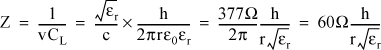
Since the speed of the signal depends on a material property, we can relate the capacitance per length of the transmission line to the instantaneous impedance. For example, if the dielectric constant is 4 and the capacitance per length of the line is 3.3 pF/inch, the instantaneous impedance of the transmission line is:
![]()
Right about now, we might be asking, what about the inductance of the line? Where does that come into play in this model? The answer is that this zeroth-order model is not an electrical model; it is a physical model. Rather than approximating the transmission line with L’s and C’s, we added the observation that the speed of the signal is the speed of light in the material.
In reality, the finite speed of the signal arises partly because of the series loop inductance of the signal and return paths. If we used a first-order, equivalent circuit model, which included the inductance per length, it would derive for us the current into the transmission line and the finite propagation speed, but the model would be more complicated mathematically.
These two models are really equivalent considering the connection between the propagation speed and the inductance per length. As we shall see, the propagation delay is directly related to the capacitance per length combined with the inductance per length. The speed of the signal has in it some assumptions about the inductance of the conductors.
7.9 Characteristic Impedance and Controlled Impedance
For a uniform line, anywhere we choose to look, we will see the same instantaneous impedance as we propagate down the line. There is one instantaneous impedance that characterizes the transmission line and we give it the special name, characteristic impedance.
Tip
There is one instantaneous impedance that is characteristic for a uniform line. We refer to this constant, instantaneous impedance as the impedance that is characteristic of the line, or the characteristic impedance of the line.
To distinguish that we are speaking of the special term the characteristic impedance of the line, which is an intrinsic property of the line, we give it the special symbol, Z0 (Z with a subscript zero). Characteristic impedance is given in units of Ohms. Every uniform transmission line has a characteristic impedance, which is one of the most important terms describing its electrical properties and how signals will interact with it.
Tip
The characteristic impedance of the line will tell us the instantaneous impedance a signal will see as it propagates down the line. As we will see, this is the chief factor that influences signal integrity in transmission line circuits.
Characteristic impedance is numerically equal to the instantaneous impedance of the line and is intrinsic to the line. It depends only on the material properties, the dielectric constant, and the capacitance per length of the line. It does not depend on the length of the line.
For a uniform line, the characteristic impedance is:
![]()
If the line is uniform, it has only one instantaneous impedance, which we call the characteristic impedance. One measure of the uniformity of the line is how constant the instantaneous impedance is down the length. If the line width varies down the line, there is no one single value of instantaneous impedance for the whole line. By definition, a nonuniform line has no characteristic impedance. When the cross section is uniform, the impedance a signal sees as it propagates down the interconnect will be constant and we say the impedance is controlled. For this reason, we call uniform cross-section transmission lines controlled-impedance lines.
Tip
We call a line that has a constant instantaneous impedance down its length a controlled-impedance line. A board that is fabricated with all its interconnects as controlled-impedance lines, all with the same characteristic impedance, is called a controlled-impedance board. All high-speed digital products, with boards larger than about 6 inches and clock frequencies greater than 100 MHz, are built with controlled-impedance boards.
When the geometry and material properties are constant down the line, the characteristic impedance of the line is uniform and one number fully characterizes the line.
A controlled-impedance line can be fabricated with virtually any uniform cross section. There are many standard cross-sectional shapes that can have controlled impedance, and many of these families of shapes have special names. For example, two round wires twisted together are called a twisted pair. A center conductor surrounded by an outer conductor is a coaxial or coax transmission line. A narrow strip of signal line over a wide plane is a microstrip. When the return path is two planes and the signal line is a narrow strip between them, we call this a stripline. The only requirement for a controlled-impedance interconnect is that the cross section be constant.
With this connection between the capacitance per length and the characteristic impedance, we can now relate our intuition about capacitance to our new intuition about characteristic impedance. We generally have a pretty good intuitive feel for capacitance and capacitance per length for the two conductors in a transmission line. If we make the two conductors wider, we increase the capacitance per length. If we move them farther apart, we make the capacitance per length lower.
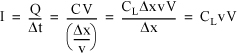
For a microstrip using FR4 dielectric, when the line width is twice the dielectric thickness, the characteristic impedance is about 50 Ohms. What happens to the characteristic impedance when we make the dielectric separation larger? It’s not obvious initially. However, we now know that the characteristic impedance of a transmission line is inversely proportional to the capacitance per length between the conductors.
Therefore, if we move the conductors farther apart, the capacitance will decrease, and the characteristic impedance will increase. Making the microstrip signal-trace wider will increase the capacitance per length and decrease the characteristic impedance. This is illustrated in Figure 7-10.
Figure 7-10 If line width increases, capacitance per length increases and characteristic impedance decreases. If dielectric spacing increases, capacitance per length decreases and characteristic impedance increases.
In general, a wide conductor with a thin dielectric will have a low characteristic impedance. For example, the characteristic impedance of the transmission line formed from the power and ground planes in a PCB will have a low characteristic impedance, generally less than 1 Ohm. Narrow conductors with a thick dielectric will have a high characteristic impedance. Signal traces, with narrow lines, will have high characteristic impedance, typically between 60 Ohms and 90 Ohms.
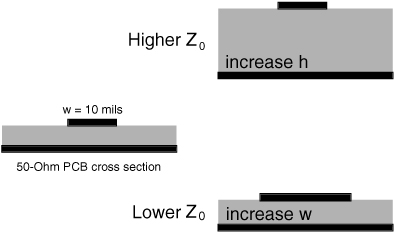
7.10 Famous Characteristic Impedances
Over the years, various specs have been established for specialized controlled-impedance interconnects. A number of these are listed in Figure 7-11. One of the most common ones is RG58. Virtually all general-purpose coax cables used in the lab, with Berkeley Nuclear Corp. (BNC) type bayonet connectors, are made with RG58 cable. This spec defines an inner- and outer-conductor diameter and a dielectric constant. In addition, when the spec is followed, the characteristic impedance is about 52 Ohms. Look on the side of the cable and you will see “RG58” stamped.
Figure 7-11 Some famous controlled-impedance interconnects based on their specified characteristic impedance.
There are other cable specs as well. RG174 is useful to know about. It is a thinner cable than RG58 and is much more flexible. When trying to snake a cable around in tight spaces or when low stress is required, the flexibility of RG174 is useful. It is specified with a characteristic impedance of 50 Ohms.
The coax cable used in Cable TV systems is specified at 75 Ohms. This cable will have a lower capacitance per length than a 50-Ohm cable and in general is thicker than a comparable 50-Ohm cable. For example, RG59 is thicker than RG58.
Twisted pairs, typically used in high-speed serial links, small computer system interconnect (SCSI) applications, and telecommunications applications, are made with 18- to 26-gauge wire. With the typical insulation thickness commonly used, the characteristic impedance is about 100 Ohms to 130 Ohms. This is typically a higher impedance than used in circuit boards, but matches the differential impedance of typical board traces. Differential impedance is introduced in a later chapter.
There is one characteristic impedance that has special, fundamental significance. This is the characteristic impedance of free space. As described previously, a signal propagating in a transmission line is really light, the electric and magnetic fields trapped and guided by the signal- and return-path conductors. As a propagating field, it travels at the speed of light in the composite dielectric medium.
Without the conductors to guide the fields, light will propagate in free space as waves. These are waves of electric and magnetic fields. As the wave propagates through space, the electric and magnetic fields will see an impedance. The impedance a wave sees is related to two fundamental constants: the permeability of free space and the permittivity of free space:
![]()
The combination of these two constants is the instantaneous impedance a propagating wave will see. We call this the characteristic impedance of free space, approximately 377 Ohms. This is a fundamental number. The amount of radiated energy from an antenna is optimized when its impedance matches the 377 Ohms of free space.
There is only one characteristic-impedance value that has fundamental significance, and it is 377 Ohms. All other impedances are arbitrary. The characteristic impedance of an interconnect can be almost any value, limited by manufacturability constraints.
But what about 50 Ohms? Why is it so commonly used? What’s so special about 50 Ohms? Its use became popular in the early 1930s when radio communications and radar systems became important and drove the first requirements for using high performance transmission lines. The application was to transmit the radio signal from the not very efficient generator to the radio antenna, with the minimum attenuation.
As we show in a later chapter, the attenuation of a coax cable is related to the series resistance of the inner conductor and outer conductor divided by the characteristic impedance. If the outer diameter of the cable is fixed, using the largest diameter cable possible, there is an optimum inner radius that results in minimum impedance.
With too large an inner radius, the resistance is lower, but the characteristic impedance is lower as well and the attenuation is higher. Too small a diameter of the inner conductor and the resistance is high and the attenuation is high. When you explore the optimum value of inner radius, you find the value for the lowest attenuation is also the value that creates 50 Ohms.
The reason 50 Ohms was chosen almost 100 years ago was to minimize the attenuation in coax cables for a fixed outer diameter. It was adopted as a standard to improve radio and radar system efficiency, and it was easily manufactured. Once adopted, the more systems using this value of impedance, the better their compatibility. If all test and measurement systems matched to this standard 50 Ohms, then reflections between instruments would be minimized and signal quality would be optimized.
In FR4, a microstrip can be fabricated if the line width is twice as wide as the dielectric is thick. There is a broad range of characteristic impedances around 50 Ohms that can also be fabricated, so it is a soft optimum.
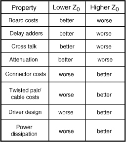
In high-speed digital systems, there are a number of trade-offs that determine the optimum characteristic impedance of the entire system. Some of these are illustrated in Figure 7-12. A good starting place is 50 Ohms. Using a higher characteristic impedance with the same pitch will mean more cross talk; however, higher-characteristic impedance connectors or twisted-pair cables will be lower cost since they are easier to fabricate. Lower characteristic impedance will mean lower cross talk and lower sensitivity to delay adders caused by connectors, components, and vias, but it also means higher power dissipation. This is important in high-speed systems.
Figure 7-12 Trade-offs in various system issues based on changing the characteristic impedance of the interconnects. Deciding on the optimum characteristic impedance, balancing performance and cost, is a difficult process. 50 Ohms is a good compromise in most systems.
Every system will have its own balance for the optimum characteristic impedance. In general, it is a very soft optimum and the exact value chosen is not critically important, as long as the same impedance is used throughout the system. Unless there is a strong driving force otherwise, 50 Ohms is usually used. In the case of Rambus memory, timing was critically important and a low impedance of 28 Ohms was chosen to minimize the impact from delay adders. To manufacture such a low impedance requires wide lines. But since the interconnect density in Rambus modules is low, the wider lines have only a small impact.
7.11 The Impedance of a Transmission Line
What impedance does a battery see connected to the front of a transmission line? As the signal propagates down the line, the current from the battery into the line is the same as the current coming out of the signal. The impedance the battery will see is thus the same as the instantaneous impedance of the line, as long as the signal is propagating down the line. The current into the line is directly proportional to the voltage applied.
A circuit element that has a constant current through it, for a constant voltage applied, is an ideal resistor. From the battery’s perspective, when the terminals are attached to the front end of the line and the signal propagates down the line, the transmission line will draw a constant current and act like a resistor to the battery. The impedance of the transmission line, as seen by the battery, is a constant resistance, as long as the signal is propagating down the line. There is no test the battery can do that will distinguish the transmission line from a resistor, at least while the signal is propagating down and back on the line.
Tip
We’ve introduced the idea of the characteristic impedance of an interconnect. We often use the terms the characteristic impedance and the impedance of a line interchangeably. But they are not always the same, and it’s important to emphasize this distinction.
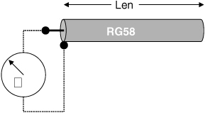
What does it mean to speak of the impedance of a cable? An RG58 cable is often referred to as a 50-Ohm cable. What does this really mean? Suppose we were to take a three-foot length of RG58 cable and measure the impedance at the front end, between the signal and return paths. What impedance will we measure? Of course, we can measure the impedance with an ohmmeter. If we connect an ohmmeter to the front end of the three-foot transmission line, between the central signal line and the outer shield, as shown in Figure 7-13, what will it read? Will it be an open, a short, or 50 Ohms?
Figure 7-13 Measuring the input impedance of a length of RG58 cable with an ohmmeter.
Let’s be more specific. Suppose we were to measure the impedance using a Radio Shack ohmmeter with a liquid crystal display (LCD) that updates in half a second. What impedance will be measured?
Of course, if we wait long enough, the short length of cable will look like an open, and we would measure infinite as the input impedance. So, if the input impedance of this short cable is infinite, what does it mean to have a 50-Ohm cable? Where does the characteristic-impedance attribute come in?
To explore this further, consider a more extreme, very long length of RG58 cable. It’s so long, in fact, that the line stretches from the earth to the moon. This is about 240,000 miles long. As we might recall from high school, the speed of light in a vacuum is about 186,000 miles per second, or close to 130,000 miles per second in the dielectric of the RG58 cable. It would take light about 2 seconds to go from one end of the cable to the far end and another 2 seconds to come back. If we attach our ohmmeter to the front end of this long line, what will it see as the impedance? Remember, the ohmmeter finds the resistance by connecting a 1-volt source to the device under test and measuring the ratio of the voltage applied to the current draw.
This is exactly the case of driving a transmission line, providing we do the impedance measurement in less than the 4-second round-trip time of flight. During the first 4 seconds, while the signal is propagating out to the end of the interconnect and back, the current into the front of the line will be a constant amount equal to the current required by the signal to charge up successive sections of the cable as it propagates outward.
The impedance the source sees looking into the front of the line, the “input” impedance, will be the same as the instantaneous impedance the signal sees, which is the characteristic impedance of the line. In fact, the source won’t know that there is an end to the line until a round-trip time of flight, or 4 seconds, later. During the first 4 seconds of measurement, the ohmmeter should read the characteristic impedance of the line, or 50 Ohms, in this case.
Tip
As long as the measurement time is less than the round-trip time of flight, the input impedance of the line, measured by the ohmmeter, will be the characteristic impedance of the line.
But, we know that if we wait a day with the ohmmeter connected, we will eventually measure the input impedance of the cable to be on open. Here are the two extremes: Initially, we measure 50 Ohms, but after a long time, we measure an open. So, what is the input impedance of the line?
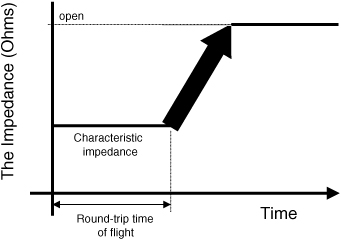
The answer is that there is no one value. It is time dependent; it changes. What this example illustrates is that the input impedance of a transmission line is time dependent; it depends on how long we are doing the measurement, compared to the round-trip time of flight. This is illustrated in Figure 7-14. Within the round-trip time of flight, the impedance looking into the front end of the transmission line is the characteristic impedance of the line. After the round-trip time of flight, the input impedance can be anywhere from infinite to zero, depending on what is at the far end of the transmission line.
Figure 7-14 The input impedance, looking into a transmission line, is time dependent. During the round-trip time of flight, the measured input impedance will be the characteristic impedance. If we wait long enough, the input impedance will look like an open.
When we refer to the impedance of a cable or a line as being 50 Ohms, we are really saying the instantaneous impedance a signal would see propagating down the line is 50 Ohms. Or, the characteristic impedance of the line is 50 Ohms. Or, initially, if we look for a time short compared to a round-trip time of flight, we will see 50 Ohms as the input impedance of the interconnect.
Even though these words sound similar, there is an important difference between the impedance, the input impedance, the instantaneous impedance, and the characteristic impedance of an interconnect. Just saying “the impedance” is ambiguous.
Tip
The input impedance of an interconnect is what a driver would measure launching a signal into the front end of the interconnect. It is time dependent. It can be an open, it can be a short, or it can be anywhere in between, all for the same transmission line, depending on how the far end is connected, how long the transmission line is, and how the impedance is measured.
The instantaneous impedance of the transmission line is the impedance the signal sees as it propagates down the line. If the cross section is uniform, the instantaneous impedance will be the same down the line. However, it may change where there are discontinuities, for example, at the end. If the end is open, the signal will see an infinite instantaneous impedance when it hits the end of the line. If there is a branch, it will see a drop in the instantaneous impedance at the branch point.
The characteristic impedance of the interconnect is a physical quality of the line that characterizes the transmission line due to its geometry and material properties. It is equal to the instantaneous impedance the signal would see as it propagates down the uniform cross section.
Everyone who works in the signal-integrity field gets lazy sometimes and just uses the term impedance. We, therefore, must ask the qualifying question of which impedance we mean, or look at the context of its use to know which of these three impedances we are referring to. Knowing the distinction, we can all try to use the right one and be less ambiguous.
When the rise time is shorter than the round-trip time of flight of an interconnect, a driver will see the interconnect with a resistive input impedance equal to the characteristic impedance of the line. Even though the line may be open at the far end, during the transition time, the front of the line will behave like a resistor.
The round-trip time of flight is related to the dielectric constant of the material and the length of the line. With rise times for most drivers in the sub-nanosecond regime, any interconnect longer than a few inches will look long and behave like a resistive load to the driver during the transition. This is one of the important reasons that the transmission line behavior of all interconnects must be considered.
Tip
In the high-speed regime, an interconnect longer than a few inches does not behave like an open to the driver. It behaves like a resistor during the transition. When the length is long enough to show transmission line behavior, the input impedance the driver sees may be time dependent. This property will strongly affect the behavior of the signals that propagate on the interconnects.
Given this criterion, virtually all interconnects in high-speed digital systems will behave like transmission lines and these properties will dominate the signal-integrity effects. For a transmission line on a board that is 3 inches long, the round-trip time of flight is about 1 nsec. If the integrated circuit (IC) driving the line has a rise time less than 1 nsec, the impedance it will see looking into the front of the line during the rising or falling edge will be the characteristic impedance of the line. The driver IC will see an impedance that acts resistive. If the rise time is very much longer than 1 nsec, it will see the impedance of the line as an open. What it sees during the transition period, as the initial edge of the signal bounces back and forth, is very complicated and can often be analyzed only using simulation tools. These tools are described later.
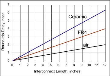
The round-trip time of flight is a very important parameter of a transmission line. To a driver, the line will seem resistive for this time. Figure 7-15 shows the round-trip time of flight for various length transmission lines made with air (εr = 1), FR4 (εr = 4), and ceramic (εr = 10) dielectric materials. In most systems with clock frequencies higher than 200 MHz, the rise time is less than 0.5 nsec. For these systems, all transmission lines longer than about 1.5 inches will appear resistive during the rise time. This means for virtually all high-speed drivers, when they drive a transmission line, during the transition the input impedance they see will act like a resistor.
Figure 7-15 For a time equal to the round-trip time of flight, a driver will see the input impedance of the interconnect as a resistive load with a resistance equal to the characteristic impedance of the line.
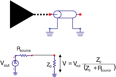
7.12 Driving a Transmission Line
For a high-speed driver launching a signal into a transmission line, the input impedance of the transmission line during the transition time will behave like a resistance that is equivalent to the characteristic impedance of the line. Given this equivalent circuit model, we can build a circuit of the driver and transmission line and calculate the voltage launched into the transmission line. The equivalent circuit is shown in Figure 7-16.
Figure 7-16 Top: Output gate driving a transmission line. Bottom: equivalent circuit model showing the voltage source, which is the driver, the output-source impedance of the driver gate itself, and the transmission line modeled as a resistor, which is valid during the round-trip time of flight of the transmission line.
The driver can be modeled as a voltage source element that switches on fast and as a source resistance. The voltage source has a voltage that is specified depending on the transistor technology. For CMOS, it ranges from 5 v to 1.5 v depending on the transistor generation. Older CMOS use 5 v, while PCI and some memory buses use 3.3 v. The fastest processors use 2.4 v and lower for their output rails and 1.5 v and lower for their core. These voltages are the supply voltages and are very close to the output voltage when the device is driving an open circuit.
The value of the source resistance also depends on the device technology. It is typically in the 5-Ohm to 60-Ohm range. When the driver suddenly turns on, some current flows through the source impedance to the transmission line and there is a voltage drop internal to the gate, before the signal comes out the pin. This means that the full-drive voltage does not appear across the output pins of the driver.
The actual voltage launched into the transmission line can be calculated by modeling this circuit as a resistive-voltage divider. The signal sees a voltage divider composed of the source resistance and the transmission line’s impedance. The magnitude of the voltage initially launched into the line is the ratio of the impedance of the line to the series combination of the line and source resistance. It is given by:
![]()
where:
Vlaunched = the voltage launched into the transmission line
Voutput = the voltage from the driver when driving an open circuit
Rsource = the output-source impedance of the driver
Z0 = the characteristic impedance of the transmission line
When the source resistance is high, the voltage launched into the line will be low—usually not a good thing. In Figure 7-17, we plot the percentage of the source voltage that actually gets launched into the transmission line and propagates down it, for a characteristic impedance of 50 Ohms. When the output-source impedance is also 50 Ohms, we see that only half the open-circuit voltage is actually launched into the line. If the output is 3.3 volts, the signal launched into the line is only 1.65 volts. This is probably not enough to reliably trigger a gate that may be connected to the line. However, as the output resistance of the driver decreases, the signal voltage into the line increases.
Figure 7-17 Amount of voltage launched into a 50-Ohm transmission line as the output source impedance of the driver varies.
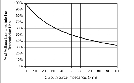
Tip
In order for the voltage, initially launched into the line, to be close to the source voltage, the driver’s output source resistance must be small—significantly less than the characteristic impedance of the line.
We say that in order to “drive a transmission line,” in other words, launch a voltage into the line that is close to the source voltage, we need an output impedance of the driver that is very small compared to the characteristic impedance of the line. If the line is 50 Ohms, then we need a source impedance less than 10 Ohms, for example.
Output devices that have exceptionally low output impedances, 10 Ohms or less, are often called line drivers, because they will be able to inject a large percentage of their voltage into the line. Older technology CMOS devices were not able to drive a line since their output impedances were in the 90-Ohm to 130-Ohm range. Since most interconnects behave like transmission lines, current-generation, high-speed CMOS devices must all be able to drive a line and are designed with low-output impedance gates.
7.13 Return Paths
In the beginning of this chapter, we emphasized that the second trace is not the ground but the return path. We should always remember that all current, without exception, travels in loops.
Tip
There is always a current loop, and if some current goes out to somewhere, it will always come back to the source.
Where is the current loop in a transmission line? Suppose we have a microstrip that is very long. In this first case, we’ll make it so long that the one-way time delay, TD, is 1 second. This is about the distance from the earth to the moon. To make it easier to think about for now, we will short the far end. We launch a signal into the line. This is shown in Figure 7-18. We said at the beginning, this meant that we had a constant current going into the signal path, related to the voltage applied and the characteristic impedance of the line.
Figure 7-18 Current injected into the signal path of a transmission line and the current distribution after a long time. When does the current actually exit the return path?
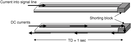
If current travels in loops and must return to the source, eventually we’d expect to see the current loop back at the end and flow back down the return path. But, how long does this take? The current flow in a transmission line is very subtle. When do we see the current come out the return path? Does it take 2 seconds—1 second to go down and 1 second to come back? What would happen then if the far end were really open? If there is insulating dielectric material between the signal and return conductors, how could the current possibly get from the signal to the return conductor, except at the far end?
The best way of thinking about it is by going back to the zeroth-order model, which describes the line as a bunch of tiny capacitors. This is shown in Figure 7-19. Consider the current flow initially. As the signal launches into the line it sees the first capacitor. As we described in an earlier chapter, if the voltage is constant, there will be no current flow through the capacitor. The only way current flows through a capacitor is if the voltage across it changes. As the signal is launched into the transmission line, the voltage across the signal- and return-path conductors ramps up. It is during this transition time, as the edge passes by, that the voltage is changing and current flows through the initial capacitor. As current flows into the signal path to charge up the capacitor, the exact same amount of current flows out of the return path, having gone through the capacitor.
Figure 7-19 Signal current gets to the return path through the distributed capacitance of the transmission line. Current is flowing only from the signal conductor to the return conductor where the signal voltage is changing—where there is a dV/dt.
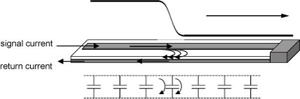
In the first picosecond, the signal has not gotten very far down the line and it has no idea how the rest of the line is configured, whether it is open, shorted, or has some radically different impedance. The current flow back to the source, through the return path, depends only on the immediate environment and the region of the line where the voltage is changing, that is, where the signal edge is.
We can extend the transmission line model to include the rest of the signal and return paths with all the various distributed capacitors between them. As the signal propagates down the line, there is current—the return current—flowing through the capacitance to the return-path conductor and looping back to the source. However, this current from the signal path, through to the return path, flows between them only where the signal voltage is changing.
A few nsec after the signal launch, near the front end, the signal voltage is constant and there is no current flow between the signal to the return path. There is just constant current flowing into the signal conductor and back out the return conductor. Likewise, in front of the signal edge, before the edge has gotten to that region of the line, the voltage is constant and there is no current flow between the signal and return paths. It is only at the signal edge that current flows through the distributed capacitance.
Once the signal is launched into the line, it will propagate down the line as a wave, at the speed of light. Current will flow down the signal line, pass through the capacitance of the line, and travel back through the return path as a loop. The front of this current loop propagates outward coincident with the voltage edge. We see that the signal is not only the voltage wave front, but it is also the current loop, which is propagating down the line. The instantaneous impedance the signal sees is the ratio of the signal voltage to the signal current.
Anything that disturbs the current loop will disturb the signal and cause a distortion, compromising signal integrity. To maintain good signal integrity, it is important to control both the current wave front and the voltage wave front. The most important way of doing this is to keep the impedance the signal sees constant.
Tip
Anything that affects the signal current or the return-current path will affect the impedance the signal sees. This is why the return path should be designed just as carefully as the signal path, whether it is on a PCB, a connector, or an IC package.
When the return path is a plane, it is appropriate to ask where does the return current flow? What is its distribution in the plane? The precise distribution is slightly frequency dependent and is not easy to calculate with pencil and paper. This is where a good 2D field solver comes in handy.
An example of the current distribution in a microstrip and a stripline for 10-MHz and 100-MHz sine waves of current is shown in Figure 7-20. We can see two important features. First, the signal current is only along the outer edge of the signal trace. This is due to skin depth. Second, the current distribution in the return path is concentrated underneath the signal line. The higher the sine-wave frequency, the more tightly concentrated this current distribution will be.
Figure 7-20 Current distribution in the signal and return paths for a microstrip and a stripline at 10 MHz and 100 MHz. In both cases, the line width is 5 mils and it is 1-ounce copper. Lighter color indicates higher current density. Results calculated with Ansoft’s 2D Extractor.
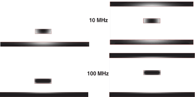
As the frequency increases, the current in the return path will take the path of lowest impedance. This translates into the path of lowest loop inductance, which means the return current will move as close to the signal current as possible. The higher the frequency, the greater the tendency for the return current to flow directly under the signal current. Even at 10 MHz, the return current is highly localized.
In general, for frequencies above about 100 kHz, most of the return current flows directly under the signal trace. Even if the trace snakes around a curvy path or makes a right-angle bend, the return current in the plane follows it. By taking this path, the loop inductance of the signal and return will be kept to a minimum.
Tip
Anything that prevents the return current from closely following the signal current, such as a gap in the return path, will increase the loop inductance and increase the instantaneous impedance the signal sees, causing a distortion.
We see that the way to engineer the return path is to control the signal path. Routing the signal path around the board will also route the return current path around the board. This is a very important principle of circuit board routing.
7.14 When Return Paths Switch Reference Planes
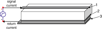
Cables are specifically designed with a return path adjacent to the signal path. This is true for coax and twisted pair cables. The return path is easy to follow. In planar interconnects found in circuit boards, the return paths are usually designed as planes, as in multilayer boards. For a microstrip, there is one plane directly underneath the signal path and the return current is easy to identify. But what if the plane adjacent to the signal path is not the plane that is being driven? What if the signal is introduced between the signal path and another plane, as shown in Figure 7-21. What will the return path do?
Figure 7-21 Driving a transmission line with the adjacent plane not being the driven return-path plane. What is the return-current distribution?
Current will always distribute so as to minimize the impedance of the signal-return loop. Right at the start of the line, the return path will couple between the bottom plane on layer 3 to the middle plane on layer 2 and then back to the signal path on layer 1.
One way to think about the currents is in the following way: The signal current in the signal path will induce eddy currents in the upper surface of the floating middle plane, and the return current in the bottom plane will induce eddy currents in the underside surface of the middle plane. These induced eddy currents will connect at the edge of the plane where the signal and return currents are being injected in the transmission line. The current flows are diagrammed in Figure 7-22.
Figure 7-22 Side view of the current flow when driving a transmission line with the adjacent plane not being the driven return-path plane.
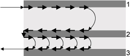
The precise current distribution in the planes will be frequency dependent, driven by skin-depth effects. In general, they will distribute in each plane to decrease the total loop inductance in the signal-return path. They can only be accurately calculated with a field solver. Figure 7-23 shows an example of the calculated current distribution, viewed from the end, for this sort of configuration for 2-mil-thick conductors at 20 MHz.
Figure 7-23 Current distribution, viewed end on, in the three conductors when the top trace and bottom plane are driven with the middle plane floating. Induced eddy currents are generated in the floating plane. Lighter colors are higher-current density. Calculated with Ansoft’s 2D Extractor.

What impedance will the driver see looking into the transmission line between the signal line and the bottom plane? The driver, driving a signal into the signal and return paths with the floating plane between them, will see two transmission lines in series. There will be the transmission line composed of the signal and plane on layer 2 and the transmission line composed of the two planes on layers 2 and 3. This is illustrated in Figure 7-24. The series impedance the driver will see is:
![]()
Figure 7-24 Top: Physical configuration of driver driving the transmission line with a floating plane between them. Bottom: Equivalent circuit model showing the impedance the driver sees as the sum of the impedance from the signal to the floating plane and between the two planes.
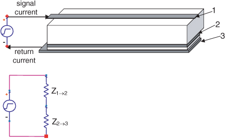
The smaller the impedance between the two planes, Z2–3, the closer to Z1–2 the driver will see as the impedance looking into this transmission line.
This means that even though the driver is connected to the signal line and the bottom plane, the impedance the driver sees is really dominated by the impedance of the transmission line formed by the signal path and its most adjacent plane. This is true no matter what the voltage of the adjacent plane is. This is a startling result.
Tip
The impedance a driver will see for a transmission line in a multilayer board will be dominated by the impedance between the signal line and the most adjacent planes, independent of which plane is actually connected to the driver’s return.
The smaller the impedance between the two planes compared to the impedance between the signal and its adjacent plane, the closer the driver will just see the impedance between the signal and floating plane.
The characteristic impedance between two long, wide planes, providing h << w, can be approximated by:
![]()
where:
Z0 = the characteristic impedance of the planes
h = the dielectric thickness between the planes
w = the width of the planes
εr = the dielectric constant of the material between the planes
For example, in FR4, for planes that are 2 inches wide with a 10-mil separation, the characteristic impedance a signal will see between the planes is about 377 Ohms × 2 × 0.01/2 = 3.8 Ohms. If the separation were 2 mils, the impedance between the planes would be 377 Ohms × 2 × 0.002/2 = 0.75 Ohm. When the plane-to-plane impedance is much less than 50 Ohms, it is less important which plane is actually DC-connected to the driver and the more likely the most adjacent planes will dominate the impedance.
Tip
The most important way to minimize the impedance between adjacent planes is to use as thin a dielectric between the planes as possible. This will keep the impedance between the planes low and provide tight coupling between the planes.
Tip
When planes are tightly coupled and there is a low impedance between them, as there should be for low rail collapse anyway, it doesn’t matter to which plane the driver actually connects. The coupling between the planes will provide a low-impedance path for the return current to get as close as possible to the signal current.
What if the signal path changes layers in mid-trace? How will the return current follow? Figure 7-25 shows a four-layer board with the signal path starting on layer 1 and transitioning through a via to layer 4. In the first half of the board, the return current must be on the plane directly underneath the signal path, on layer 2. In addition, for sine-wave-frequency components of the current above 10 MHz, the current is actually flowing on the top surface of the layer 2 plane.
Figure 7-25 Cross section of a four-layer board with signal current transitioning from layer 1 to layer 4 through a via. How does the return current transition from layer 2 to layer 3?
In the bottom half of the board, where the signal is on layer 4, where will the return current be? It has to be on the plane adjacent to the signal layer, or on plane layer 3. And, it will be on the undersurface of the plane. In the regions of uniform transmission line, the return currents are easy to follow. The via is clearly the path the signal current takes to go from layer 1 to layer 4. How does the return current make the transition from layer 2 to layer 3?
If the two planes are at the same potential and have a via shorting them, the return current would take this path of low impedance. There might be a small jog for the return current, but it would be through a short length of plane, and a plane has low total inductance so would not have a large impedance discontinuity. This would be the preferred stack-up. If there were no other constraints such as cost, keeping the nearest reference planes at the same voltage and shorting them together close to the signal via is the optimum design rule. To reduce the voltage drop in the return path, always consider adding a return via adjacent to the signal via.
However, to minimize the total number of layers, it is sometimes necessary to use adjacent reference layers with different voltages. If plane 2 is a 5-v plane and plane 3 is a 0-v plane, there would be no DC path between them. How will the return current flow from plane 3 to plane 2?
It can only go through the capacitance between them. At the clearance hole, the return current will snake around and change surfaces on the same plane. The return current will then spread out on the inner surfaces of the planes and couple through the plane-to-plane capacitance. The current will spread out between the planes at the speed of light in the dielectric. The current flows in the return path are shown in Figure 7-26. The two return-path planes create a transmission line, and the return current will see an impedance that is the instantaneous impedance of the two planes.
Figure 7-26 The return current transitions from layer 2 to layer 3 by capacitive coupling between the layers.
Tip
Whenever the return-path current switches planes and the planes are DC isolated, the return current will couple through the planes and see an impedance equal to the instantaneous impedance of the transmission line created by the planes.
The return current will have to go through this impedance and there will be a voltage drop in the return path. We call this voltage drop in the return path ground bounce. The larger the impedance of the return path, the larger the voltage drop, and the larger the ground-bounce noise generated. All other signal lines that are also changing reference planes will contribute to this ground-bounce voltage noise and encounter the ground-bounce noise created by the other signals.
Tip
The goal in designing the return path is to minimize the impedance of the return path to minimize the ground-bounce noise generated in the return path. As we will see, this is primarily implemented by keeping the impedance between the return planes as low as possible, usually by keeping them on adjacent layers with as thin a dielectric as possible between them.
As the return current spreads out between the two return-path planes in an ever-expanding circle from the signal via, it will see an ever-decreasing instantaneous impedance. The capacitance per length that the signal sees gets larger as the radius gets larger. This makes the analysis complicated except for specific cases and in general, requires a field solver.
However, we can build a simple model to estimate the instantaneous impedance between the two planes and to provide insight into how to optimize the design of a stack-up and minimize this form of ground bounce.
To calculate the instantaneous impedance the signal sees as it propagates radially outward between the two planes, we need to calculate the capacitance per length of the radial-transmission line and the speed of the signal. The capacitance per length the signal will see is the change in capacitance per incremental change in radius. The total capacitance the return current sees is:
![]()
and the area between the planes is:
![]()
Combining these relationships shows the capacitance increasing with distance as:
![]()
where:
C = the coupling capacitance between the planes
ε0 = permittivity of free space, 0.225 pF/in
εr = the dielectric constant of the material between the planes
A = the area of overlap of the return current in the planes
h = the spacing between the planes
r = the increasing radius of the coupling circle, expanding at the speed of light
The incremental increase in capacitance as the radius increases (i.e., the capacitance per length) is:
![]()
As expected, as the return current moves farther from the via, the capacitance per length increases. The instantaneous impedance this current will see is:
where:
Z = the instantaneous impedance the return current sees between the planes
CL = the coupling capacitance per length between the planes
v = the speed of light in the dielectric
ε0 = permittivity of free space, 0.225 pF/in
εr = the dielectric constant of the material between the planes
h = the spacing between the planes
r = the increasing radius of the coupling circle, expanding at the speed of light
c = the speed of light in a vacuum
For example, if the dielectric thickness between the planes is 10 mils, the impedance the return current will see by the time it is 1 inch away from the via is Z = 60 × 0.01/(1 × 2) = 0.3 Ohm. And, this impedance will get smaller as the return current propagates outward. This says that the farther from the via, the lower the impedance the return current sees, and the lower the ground-bounce voltage will be across this impedance.
We can relate the impedance the return current sees (which is the impedance in series with the signal current) to time, since the return current spreads out at the speed of light in the material and r = v × t:
![]()
where:
Z = the instantaneous impedance the return current sees between the planes, in Ohms
v = the speed of light in the dielectric
εr = the dielectric constant of the material between the planes
c = the speed of light in a vacuum
h = the spacing between the planes, in inches
t = the time the return current is propagating, in nsec
For example, for a spacing of 0.01 inch, the impedance the return current sees after the first 0.1 nsec is Z = 5 × 0.01/0.1 = 0.5 Ohm. The very first leading edge of the signal will see an initial impedance that can be as large as 0.5 Ohm. If the signal current were 20 mA in the first 100 psec, corresponding to a 1-v signal in a 50-Ohm impedance, the ground-bounce voltage drop across the switching planes that are in series with the signal voltage, for the first 0.1 nsec, would be 20 mA × 0.5 Ohm = 10 mV.
This may not seem like a lot compared to the 1-v signal, but if 10 signals transition simultaneously between the same reference planes, all within less than 0.6 inch of each other, they will each see the same common 0.5-Ohm impedance and there will be 20 mA × 10 = 200 mA of current through the return-path impedance. This will generate a ground-bounce noise of 200 mA × 0.5 Ohm = 100 mV, which is now 10% of the signal voltage and can be significant. All signal paths that also transition through this path will see the 100 mV of ground-bounce noise, even if they are not switching.
The initial impedance the return current will see can be high, if there is substantial current flowing in a very short time initially. All current flowing during this initial short time will see a high impedance and generate ground-bounce voltages. Figure 7-27 shows the impedance the return current sees over time. From this plot, it is clear that the impedance of the return path is significant only for very fast rise times, substantially less than 0.5 nsec.
Figure 7-27 The impedance the return current sees between the planes for 2-mil spacing and 10-mil spacing, as the signal propagates outward from the via.

When the impedance is significant—about 5% of 50 Ohms—for one signal line switching, the impedance of the return path is important. When there are n signal paths switching through these planes, the maximum acceptable impedance of the return path is 2.5 Ohms/n.
Tip
This analysis indicates that for fast edges and multiple signals switching simultaneously between reference planes, significant ground-bounce voltage can be generated across the return path. The only way to minimize this ground-bounce voltage is by decreasing the impedance of the return path.
This is primarily accomplished by:
1. Make sure that as the signal path transitions layers, it always has an adjacent plane with the same voltage level for its reference and there is a shorting via between the switching planes in close proximity to any signal vias.
2. Keep the spacing between different DC-voltage-level reference planes as thin as possible.
3. Space out adjacent switching vias so that the return currents do not overlap during the initial transients when the impedance of the return path can be high.
It is sometimes believed that adding a decoupling capacitor between two reference planes for which there is a switching return current will help to decrease the impedance of the return path. It is hoped the added discrete capacitor will provide a low-impedance path for the return current to flow from one reference plane to the other.
Tip
To provide any effectiveness, the real capacitor must keep the impedance between the planes less than 5% × 50 Ohms or 2.5 Ohms, at the bandwidth of the rise time’s frequency components.
A real capacitor has some loop inductance and some equivalent series resistance associated with it. This will limit the usefulness of discrete decoupling capacitors for very short rise-time signals. After all, the impedance between the planes will already be low after long periods or for the low-frequency components.
For the higher-frequency components that could use a discrete component, it is not the capacitance that determines the real capacitor’s impedance; it is its equivalent series inductance. Figure 7-28 shows the expected impedance of a real 1-nF capacitor with a loop inductance of 0.5 nH. This is an extremely optimistic loop inductance and can only be achieved by either a multiple via in-pad configuration or with the use of interdigitated capacitors (IDCs).
Figure 7-28 Impedance of a capacitor with 1-nF capacitance and only 0.5 nH of loop inductance.
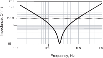
This real capacitor will provide a low impedance for the return path for signal bandwidths only up to 1 GHz. Higher capacitance than 1 nF will provide no added value, since the low-frequency components will see a low impedance between the planes anyway.
Tip
When using a discrete capacitor to decrease the impedance of the return path, it is far more important to keep the series inductance low than to use more than 1 nF of capacitance.
Unfortunately, even the 0.5 nH of loop inductance of a well-designed capacitor will still have a large impedance at frequencies above 1 GHz, where the planes do not have low impedance and their ground bounce may be a problem.
Tip
A capacitor between different DC-voltage planes will not be very effective at managing the ground bounce from switching planes. It may, however, provide additional decoupling for lower-frequency noise but will not solve the ground-bounce problem as rise times continue to decrease.
Tip
In a multilayer board, when signal paths must change different voltage-level reference layers, the only way of minimizing the ground-bounce voltage generated is by using a dielectric between the reference planes that is as thin as possible.
There is one additional problem created when a signal changes reference planes and current is driven in the transmission line formed by the two adjacent planes. Where does this current end up? As the current propagates outward, eventually it will hit the edges of the board. The current injected between the planes when the signal current switches will rattle around between the planes, causing transient voltages between the two planes.
The impedance between the planes is very low, much less than 1 Ohm, so the transient voltages created will be low. However, with multiple signals switching between planes, each one injects some noise between the planes. This noise will get larger with more signals switching. The current injected into the planes is determined by the signal impedance, roughly 50 Ohms. The voltage noise generated between the planes depends on the impedance of the planes. To minimize this rattling voltage, the impedance of the planes should be kept to a minimum by keeping their spacing thin.
Signals transitioning reference planes is a dominant source of noise injected between the planes. This voltage noise will rattle around and contribute to the noise in the PDN. In low noise systems, it can be a major source of cross talk to very sensitive lines, such as rf receivers or analog to digital converter inputs or voltage references. To minimize the noise in these systems, care should be taken to minimize the return current injected between the planes by the careful selection of return plane voltages, return vias, and low inductance decoupling capacitors.
We sometimes call this voltage, which is rattling between the edges of the board between the adjacent plane layers, resonances in the planes. These resonances will eventually die out from conductor and dielectric attenuation. They will have frequency components that match the round-trip time of flight between the board dimensions. For boards with a dimension of 10–20 inches on a side, the resonant frequencies will be in the 150-MHz to 300-MHz range. This is why capacitors between the different voltage planes can provide some value. They help to maintain a low impedance between the planes (in the board resonant-frequency range) and keep the voltages between the planes low. However, as we saw, they do not affect the transient ground-bounce voltage during the very fast transition.
Tip
To minimize the resonant rattling-around voltage, especially in small multilayer packages, it is important to avoid having any return currents switch between different reference voltage layers. The adjacent return layers should be at the same DC-voltage level, and a return via should connect the return path in proximity to the signal via. This will avoid injecting any currents between planes and avoid driving any plane resonances.
These problems will get more important as rise times decrease, especially below 100 psec.
7.15 A First-Order Model of a Transmission Line
An ideal transmission line is a new ideal circuit element that has the two special properties of a constant instantaneous impedance and a time delay associated with it. This ideal model is a “distributed” model in the sense that the properties of an ideal transmission line are distributed over its length rather than being concentrated in a single lumped point.
Physically, a controlled-impedance transmission line is composed of just two conductors with length and having a uniform cross section for the whole length. Earlier in this chapter, we introduced a zeroth-order model, which described a transmission line as a collection of capacitors spaced some distance apart. This was a physical model, not an equivalent electrical model.
We can further approximate the physical transmission line by describing the sections of signal- and return-path conductors as a loop inductance. The simplest equivalent circuit model for a transmission line would have small capacitors separated by small loop inductors, as shown in Figure 7-29. The C is the capacitance between the conductors and the L is the loop inductance between the sections.
Figure 7-29 Top: physical structure of a uniform transmission line. Bottom: first-order equivalent circuit model approximation for a transmission line based on combinations of L’s and C’s.
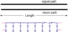
Each segment of the signal path has some partial self-inductance associated with it, and each segment of the return path has some partial self-inductance associated with it. There is some partial mutual inductance between each of the signal- and return-path segments between the discrete capacitors. For an unbalanced transmission line, such as a microstrip, the partial self-inductances of the signal- and return-path segments are different. In fact, the partial self-inductance of the signal path can be more than 10 times larger than the partial self-inductance of the return path.
However, from a signal’s perspective as it propagates down the line, it is a current loop, from the signal to the return path, that propagates. In this sense, all the signal current sees is the loop inductance down the signal-path segment and returning back through the return-path segment. For signal propagation in a transmission line and most cross-talk effects, the partial inductances of the signal and return paths do not play a role. It is only the loop inductance that is important. When approximating an ideal distributed-transmission line as a series of LC segments, the inductance the signal sees, as represented in the model, is really a loop inductance.
Tip
It is important to keep in mind that this lumped circuit model is an approximation of an ideal transmission line. In the extreme case, as the size of the capacitors and inductors gets diminishingly small and the number of each increases, the approximation gets better and better.
In the extreme, when each capacitor and inductor is infinitesimal and there is an infinite number of elements, there is a uniform capacitance per length, CL, and a uniform loop inductance per length, LL. These are often called the line parameters of a transmission line. Given the total length of the line, Len, the total capacitance is given by:
![]()
and the total inductance is given by:
![]()
where:
CL = capacitance per length
LL = loop inductance per length
Len = length of the transmission line
Just by looking at this LC circuit, it is difficult to get a feel for how a signal will interact with it. At first glance, we might think there will be a lot of oscillations and resonances. But what happens when the size of each element is infinitely small?
The only way to really know how a signal will interact with this circuit model is to apply network theory and solve the differential equations represented by this LC network. The results indicate that a signal traveling down the network will see a constant instantaneous impedance at each node. This constant instantaneous impedance is the same as the instantaneous impedance we discovered for an ideal distributed-transmission-line element. The instantaneous impedance is numerically the characteristic impedance of the line. Likewise, there will be a finite delay between the time the signal is introduced into the front of the LC network and the time it comes out.
Using network theory, we can calculate how the characteristic impedance and time delay depend on the line parameters and total length of the line:
![]()
![]()
![]()
where:
Z0 = the characteristic impedance, in Ohms
LL = the loop inductance per length of the transmission line
CL = the capacitance per length of the transmission line
TD = the time delay of the transmission line
Ltotal = the total loop inductance in the transmission line
Ctotal = the total capacitance in the transmission line
v = the speed of the signal in the transmission line
Without having to invoke a finite speed for the propagation of a signal down a transmission line, the electrical properties of an LC network predict this behavior. Likewise, though it is hard to tell looking at the circuit model, network theory predicts there is a constant impedance the signal sees at each node along the circuit.
These two predicted properties (the characteristic impedance and the time delay) must match the same values we derived based on the zeroth-order physics model of finite speed and collection of capacitor buckets. By combining the results from these two models, a number of very important relationships can be derived.
Because the speed of a signal depends on the dielectric constant of the material and on the capacitance per length and inductance per length, we can relate the capacitance per length to the inductance per length:
![]()
![]()
![]()
From the relationship between the characteristic impedance and velocity, the following relationships can be derived:
![]()
![]()
And, from the time delay and the characteristic impedance of the transmission line, the following can be derived:
![]()
![]()
Z0 = the characteristic impedance, in Ohms
LL = the loop inductance per length of the transmission line, in nH/inch
CL = the capacitance per length of the transmission line, in pF/inch
TD = the time delay of the transmission line, in nsec
Ltotal = the total loop inductance in the transmission line, in nH
Ctotal = the total capacitance in the transmission line, in pF
v = the speed of the signal in the transmission line, in in/nsec
For example, a line that is 50 Ohms and has a dielectric constant of 4 has a capacitance per length of CL = 83/50 × 2 = 3.3 pF/inch. This is a startling conclusion.
Tip
All 50-Ohm transmission lines with a dielectric constant of 4 have the same capacitance per length—about 3.3 pF/inch. This is a very useful rule of thumb to remember.
If the line width doubles, the dielectric spacing would have to double to maintain the same characteristic impedance, and the capacitance would stay the same. An interconnect in a BGA package that has been designed as a 50-Ohm controlled-impedance line, 0.5 inches long, has a capacitance of 3.3 pF/inch × 0.5 inch = 1.6 pF.
Likewise, the inductance per length of a 50-Ohm line made with FR4 is LL = 0.083 × 50 × 2 = 8.3 nH/inch.
Tip
All 50-Ohm transmission lines with a dielectric constant of 4 have the same loop inductance per length of about 8.3 nH/inch. This is a very useful rule of thumb to remember.
If the time delay of a line is 1 nsec and it is 50 Ohms, the total capacitance in the line is Ctotal = 1 nsec/50 = 20 pF. If the line is 6 inches long, this 20 pF of capacitance is distributed over 6 inches and the capacitance per length is 20 pF/6 inches = 3.3 pF/inch. For this same line, the total loop inductance going down the signal line and looping back through the return path is Ltotal = 1 nsec × 50 Ohms = 50 nH. Distributed over the 6 inches of length, this is an inductance per length of 50 nH/6 inches = 8.3 nH/inch.
These relationships that relate the capacitance, inductance, characteristic impedance, and dielectric constant, which are associated with a transmission line, apply to any transmission line. They make no assumptions on the cross-section geometry. They are very powerful tools to help us estimate one or more of these terms using existing approximations or field solvers. If we know any two, we can always find the others.
7.16 Calculating Characteristic Impedance with Approximations
Engineering a particular target characteristic impedance is really a matter of adjusting the line widths, dielectric thickness, and dielectric constants. If we know the length of the transmission line and the dielectric constant of the material around the conductors and we can calculate the characteristic impedance, we can use the relationships above to calculate all other parameters.
Of course, every different type of cross-sectional geometry will have a different relationship between the geometrical features and the characteristic impedance. In general, there are three types of analysis we can use to calculate the characteristic impedance from the geometry:
1. Rules of thumb
2. Approximations
3. 2D field solvers
The two most important rules of thumb relate the characteristic impedance of a microstrip and stripline fabricated with FR4. The cross sections for 50-Ohm transmission lines are illustrated in Figure 7-30.
Figure 7-30 Scaled cross sections for 50-Ohm transmission lines in FR4. Left: 50-Ohm microstrip has w = 2 × h. Right: 50-Ohm stripline has b = 2 × w.
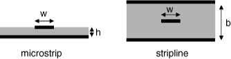
Tip
As a good rule of thumb, a 50-Ohm microstrip in FR4 has a line width twice the dielectric thickness. A 50-Ohm stripline has a total dielectric spacing between the planes equal to twice the line width.
There are only three cross-section geometries that have exact equations. All others are approximations. These three are coax, twin-round-wire, and round-wire-over-plane geometries. They are illustrated in Figure 7-31. The relationship between characteristic impedance and geometry for a coax is:
![]()
Figure 7-31 The only three cross sections for which there are exact equations for the characteristic impedance. All others are approximations.

For twin parallel round wires, the characteristic impedance is:
![]()
For the case of a round rod over a plane, the characteristic impedance is:
![]()
where:
Z0 = the characteristic impedance, in Ohms
a = inner radius of the coax, in inches
b = outer radius of the coax, in inches
r = radius of the round rod, in inches
s = center-to-center spacing of the round rod, in inches
h = height of the center of the rod over the plane, in inches
εr = dielectric constant of the materials
These relationships assume the dielectric material completely and uniformly fills all space wherever there are electric fields. If this is not the case, the effective dielectric constant that affects the speed of the signal down the conductor will be some complicated combination of the mixture of dielectrics. This can often only be calculated with a field solver.
For homogeneous dielectric distributions, these are useful relationships to use to calibrate 2D field solvers, since they are exact.
Tip
With very few exceptions, virtually all other equations used to relate the characteristic impedance to the geometry are approximations. When being off by more than 5% may increase design-time and costs excessively, approximations should not be used for final sign-off of the design of transmission lines. When accuracy counts, a verified 2D field solver should be used.
The value of approximations is that they show the relationship between the geometrical terms and can be used for sensitivity analysis in a spreadsheet. The most popular approximation for microstrip recommended by the IPC is:
![]()
For stripline, the IPC recommended approximation is:
![]()
where:
Z0 = characteristic impedance, in Ohms
h = dielectric thickness below the signal trace to the plane, in mils
b = plane-to-plane spacing, in mils
t = metal thickness, in mils
εr = dielectric constant
If we ignore the impact from the trace thickness, t, then the characteristic impedance for both structures depends only on the ratio of the dielectric thickness to the line width. This is a very important relationship.
Tip
To first order, the characteristic impedance of stripline and microstrip will scale with the ratio of the dielectric thickness to the line width. As long as this ratio is constant, the characteristic impedance will be constant.
For example, if the line width is doubled and the dielectric spacing is doubled, the characteristic impedance will be unchanged to first order.
Though these equations look complicated, this is no measure of accuracy. The only way to know the accuracy of an approximation is to compare it to the results from a verified field solver.
7.17 Calculating the Characteristic Impedance with a 2D Field Solver
If we need better than 10% accuracy or are worrying about second-order effects, such as the effect of trace thickness, solder-mask coverage, or side-wall shape, we should not be using one of these approximations. The most important tool that should be in every engineer’s toolbox for doing impedance calculations is a 2D field solver.
The basic assumption made by all 2D field solvers is that the geometry is uniform. That is, as we move down the length of the transmission line, the cross-sectional geometry stays the same. This is the basic definition of a controlled-impedance line—that the cross section is uniform. In such a case, there is only one characteristic impedance that describes the line. This is why a 2D field solver is the right tool to provide an accurate prediction of the characteristic impedance of uniform transmission lines. Only the 2D cross-sectional information is important.
Whenever accuracy is important, a 2D field solver should be used. This means that before sign-off on a design and committing to hardware, the stack-up should be designed with a 2D field solver. Sometimes the argument is made, if the manufacturing tolerance is 10%, that we should not care if the accuracy of the prediction is even 5%.
Accuracy is important because of yield. Any inaccuracy in the predicted impedance will shift the center position of the distribution of the manufactured impedances. The better we can center the distribution on the required target, the better we can increase yield. Even an inaccuracy of 1% will shift the distribution off center. Any product close to the spec limits could be shifted outside the limits and contribute to a yield hit. As we showed in an earlier chapter, the accuracy of a field solver can be better than 0.5%.
Using a 2D field solver, the characteristic impedance of a microstrip can be calculated. These results are compared to the predictions based on the IPC approximations. Figure 7-32 shows the predicted characteristic impedance of a microstrip with dielectric constant of 4, with 1/2-ounce copper and dielectric thickness of 10 mils, as the line width is varied. Near and above 50 Ohms, the agreement is very good. However, for lower impedances, the IPC approximation can be off by as much as 25%.
Figure 7-32 Comparison of field-solver results (circles) and the IPC approximation (line) for a microstrip with 10-mil-thick FR4 dielectric and 1/2-ounce copper. Field-solver results from the Ansoft 2D Extractor.
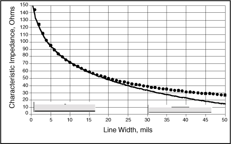
The same comparison is made for stripline and is shown in Figure 7-33. The agreement close to 50 Ohms is very good, but for low impedances, the approximation can be off by more than 25%. Approximations should not be used when accuracy counts.
Figure 7-33 Comparison of field-solver results (circles) and the IPC approximation (line) for a stripline with 10-mil-thick FR4 dielectric and 1/2-ounce copper. Field-solver results from the Ansoft 2D Extractor.
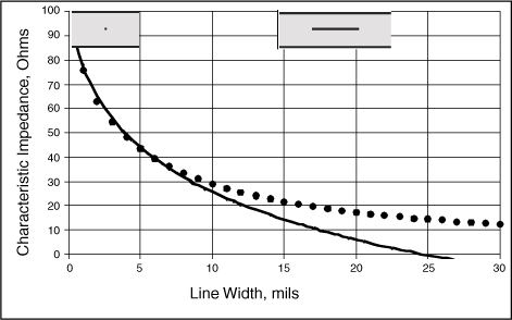
In addition to providing an accurate estimate for the characteristic impedance, a 2D field solver can also provide insight into the impact from second-order effects, such as:
1. The width of the return path
2. The thickness of the signal-trace conductor
3. The presence of solder mask over a surface trace
4. The effective dielectric constant
How does the width of the return path influence the characteristic impedance? If the width of the return path is narrow, the capacitance should be smaller and the characteristic impedance would be higher. Using a field solver we can calculate how wide the return path has to be so that it doesn’t matter anymore.
Figure 7-34 shows the calculated characteristic impedance of a microstrip with dielectric constant of 4 and trace thickness of 0.7 mil, corresponding to 1/2-ounce copper, dielectric thickness of 5 mils, and line width of 10 mils. This is nominally a 50-Ohm line. The width of the return path is varied and the characteristic impedance calculated. If the width of the extension on each side of the signal trace is greater than 15 mils, the characteristic impedance is less than 1% off from its infinite width value. Because the fringe fields along the edge of the trace scale with the dielectric thickness, this is the important scale factor. The extent of the return path on either side of the signal path should be roughly 3 times the dielectric thickness, h.
Figure 7-34 Top: calculated characteristic impedance of a microstrip with 10-mil-wide trace and 5-mil-thick dielectric, as the return-path plane is widened. Bottom: variation from the nominal value. Field solver results from the Ansoft 2D Extractor.
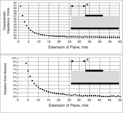
Tip
As a rough rule of thumb, the return path should extend at least three times the dielectric thickness on either side of the signal trace for the characteristic impedance to not exceed more than 1% of the value when the return path is infinitely wide.
Using a 2D field solver, we can calculate the characteristic impedance as the trace thickness changes from 0.1 mil thick to 3 mils thick. This is plotted in Figure 7-35. Each point on the curve is the calculated characteristic impedance for a different trace thickness. It can be seen that as the metal thickness increases, the fringe field capacitance increases and the characteristic impedance decreases, as we would expect. Thicker metal means higher capacitance between the signal trace and the return path, which also means lower characteristic impedance. However, as we can see from the calculated results, this is not a large effect—it is second order.
Figure 7-35 Calculated characteristic impedance of a nominal 50-Ohm microstrip as the trace thickness is changed. The circles are calculated results; the line is 2 Ohms/mil. Field solver results from the Ansoft 2D Extractor.

Tip
As a rough rule of thumb, the decrease in characteristic impedance is about 2 Ohms per mil of signal-trace thickness.
If there is a thin solder-mask coating on top of the microstrip, the fringe field capacitance will increase and the characteristic impedance will decrease. For the same microstrip as above, but using a conductor only 0.1 mil thick, the characteristic impedance is calculated for an increasing solder-mask coating, using a dielectric constant of 4. Figure 7-36 shows the decrease in characteristic impedance. It is about 2 Ohms/mil of coating for thin coatings. After about 10-mil-thick coating, the characteristic impedance is no longer affected, as all the external fringe fields are contained in the first 10 mils of coating. This is a measure of how far the fringe fields extend above the surface.
Figure 7-36 Calculated characteristic impedance of a nominal 50-Ohm microstrip as a solder mask with dielectric constant of 4 is added. Circles are the field solver results; the line is 2 Ohms/mil. Field solver results from the Ansoft 2D Extractor.

Of course, solder mask is more typically 0.5 mil to 2 mils. In this regime, we see that the presence of the solder mask can lower the characteristic impedance by as much as 2 Ohms, a significant amount. To reach a target impedance with solder mask requires the line width to be narrower than nominal so the solder mask would bring the impedance back down to the target value.
This last example illustrates that the characteristic impedance depends on the dielectric distribution above the trace in a microstrip. Of course, in a stripline, all the fields are contained by the dielectric so solder mask on top of the upper plane has no impact on the characteristic impedance.
In addition to the characteristic impedance affected by the inhomogeneous dielectric distribution, the effective dielectric constant the fields experience is also affected by the dielectric distribution. In microstrip, the effective dielectric constant, which determines the speed of the signal, depends on the specific geometry of the dielectric. Often, the effective dielectric constant can only be accurately calculated with a field solver. This was discussed in detail in an earlier chapter.
7.18 An n-Section Lumped Circuit Model
The ideal transmission-line circuit element is a distributed element that very accurately predicts the measured performance of real interconnects. Figure 7-37 shows the comparison of the measured and simulated impedance of a 1-inch-long transmission line, in the frequency domain. We see the excellent agreement even up to 5 GHz, the bandwidth of the measurement.
Figure 7-37 Measured (circles) and simulated (line) impedance of a 1-inch-long, 50-Ohm transmission line. The model is an ideal, lossless transmission line. The agreement is excellent up to the bandwidth of the measurement.
Tip
Real interconnects match the behavior of an ideal transmission line to high bandwidth. An ideal transmission line is a very good model for real interconnects.
We can approximate this ideal model by a combination of LC lumped-circuit sections. The question naturally arises, how do we know how many LC sections to use for a given level of accuracy and what happens if we use too few sections?
These questions can be explored using a simulation tool like SPICE. We will first work in the frequency domain to evaluate the impedance looking into the front end of a transmission line and then interpret this result in the time domain.
In the frequency domain, we can ask what is the impedance looking into the front end of a transmission line, with the far end open. In this example, we will use a 50-Ohm line that is 6 inches long with a dielectric constant of 4. Its time delay, TD, is 1 nsec.
The total capacitance is given by Ctotal = TD/Z0 = 1 nsec/50 Ohms = 20 pF. The total loop inductance is given by Ltotal = Z0 × TD = 50 Ohms × 1 nsec = 50 nH.
The simplest approximation for a transmission line is a single LC model, with the L and C values as the total values of the transmission line. This is the simplest lumped circuit model for an ideal transmission line.
Figure 7-38 shows the predicted impedance for an ideal, distributed transmission line and the calculated impedance of a single-section LC lumped-circuit model using these values. In the low-frequency range, the LC model matches the performance really well. The bandwidth of this model is about 100 MHz. The limitation to the bandwidth is because, in fact, this ideal transmission line does not have all its capacitance in one place. Instead, it is distributed down the length, and between each capacitor is some loop inductance associated with the length of the sections. However, it is clear from this comparison that a transmission line, open at the far end, will look exactly like an ideal capacitor at low frequency.
Figure 7-38 Simulated impedance of an ideal transmission line (circles) and simulated impedance of a single-section LC lumped-circuit model (line). The agreement is excellent up to the bandwidth of about 100 MHz.
The impedance of the ideal transmission line shows the resonance peaks occurring when the frequency matches another half wavelength that can fit in the length of the transmission line. The peak resonant frequencies, fres, are given by:
![]()
where:
fres = the frequency for the peaks in the impedance
m = the number of the peak, also the number of half waves that fit in the transmission line
TD = the time delay of the transmission line
f0 = the frequency at which one complete wave fits in the transmission line
The first resonance for m = 1 is for 1 × 1 GHz/2 = 0.5 GHz. Here, just one half wave will fit evenly in the length of the transmission line, with a TD of 1 nsec. The second resonance for m = 2 is at 2 × 1 GHz/2 = 1 GHz. Here, exactly one wave will fit in the transmission line. These standing wave patterns are shown in Figure 7-39.
Figure 7-39 Voltage waves on the transmission line. Resonances are when an additional half wavelength can fit in the line.
The bandwidth of the single-section LC model is about one quarter the frequency of the first resonance, up to about 125 MHz. We can improve the bandwidth of the model by breaking the transmission line into more sections. If we break it up in two sections, then each section can be modeled as an identical LC model and the values of each L and C would be Ltotal/2 and Ctotal/2. The predicted impedance of this two-section LC model compared with the ideal T line is shown in Figure 7-40. The bandwidth of this model is roughly at half the first resonance peak. This is a frequency of about 250 MHz.
Figure 7-40 Simulated impedance of an ideal transmission line (circles) and simulated impedance of a one-section and two-section LC lumped-circuit model (lines).
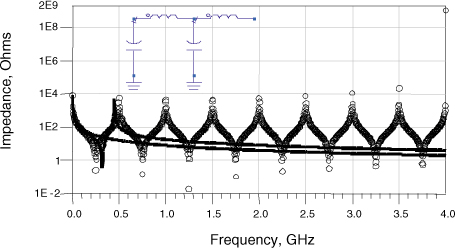
We can further increase the bandwidth of this lumped circuit model by breaking up the length into more LC sections. Figure 7-41 shows the comparison with an ideal transmission line and using 16 different LC sections, with each L and C being Ltotal/16 and Ctotal/16. As we increase the number of sections, we are able to better approximate, to a higher bandwidth, the impedance behavior of an ideal transmission line. The bandwidth of this model is about up to the fourth resonance peak, at 2 GHz.
Figure 7-41 Simulated impedance of an ideal transmission line (circles) and simulated impedance of a 16-section LC lumped-circuit model (line).
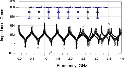
Tip
An n-section LC circuit is an approximation of an ideal transmission line. The more sections, the higher the bandwidth of the approximation.
We can estimate the bandwidth of an n-section lumped-circuit model based on the time delay of this ideal transmission line. These last examples illustrate that the more segments in the LC model, the higher the bandwidth. One section has a bandwidth up to one quarter of the first resonant peak; two sections up to half the first resonance; and 16 sections up to the second resonant frequency. We can generalize that the highest frequency at which we have good agreement—the bandwidth of the model—is:
![]()
or
![]()
where:
BWmodel = the bandwidth of the n-section lumped-circuit model
n = the number of LC sections in the model
TD = the time delay of the transmission line
f0 = the resonant frequency for one complete wavelength = 1/TD
We have approximated the relationship to be a little more conservative and a little easier to remember by using n = 10 × BWmodel × TD, rather than n = 8 × BWmodel × TD.
Tip
This is a very important rule of thumb to keep in mind. It says, to reach a bandwidth of the model equal to the 1/TD, 10 LC sections are required. It also says that because this frequency corresponds to having one wavelength in the transmission line, for a good approximation, there should be one LC section for every 1/10th wavelength of the signal.
For example, if the interconnect has a TD = 1 nsec, and we would like an n-section LC model with a bandwidth of 5 GHz, then we need at least n = 10 × 5 GHz × 1 nsec = 50 sections. At this highest frequency, there will be 5 GHz × 1 nsec = 5 wavelengths on the transmission line. For each wave, we need 10 sections; therefore, we need 5 × 10 = 50 LC sections for a good approximation.
If the TD of a line is 0.5 nsec and we need a bandwidth of 2 GHz, the number of sections required is n = 10 × 2 GHz × 0.5 nsec = 10 sections.
We can also evaluate the frequency to which we can use a single LC section to model a transmission line. In other words, up to what frequency does a transmission line look like a simple LC circuit? The bandwidth of one section is:
![]()
For the case of a transmission line with a TD = 1 nsec, the bandwidth of a single-section LC model for this line is 0.1 × 1/1 nsec = 100 MHz. If the TD = 0.16 nsec, (roughly 1 inch long), the bandwidth of a simple LC model for this line is 0.1 × 1/0.16 nsec = 600 MHz. The longer the time delay of a transmission line, the lower the frequency at which we can approximate it as a simple LC model.
We have evaluated the number of sections we need to describe a transmission line for a required bandwidth. We found that we needed about 10 LC sections per wavelength of the highest frequency component of the signal and a total number of LC segments depending on the number of wavelengths of the highest frequency component of the signal that can fit in the transmission line.
If we have a signal with a rise time, RT, the bandwidth associated with the signal (the highest sine-wave frequency component that is significant) is BWsig = 0.35/RT. If we have a transmission line that has a time delay of TD and we wish to approximate it with an n-section lumped-circuit model, we need to make sure the bandwidth of the model, BWmodel, is at least > BWsig:
![]()
![]()
![]()
where:
BWsig = bandwidth of the signal
BWmodel = the bandwidth of the model
RT = the rise time of the signal
TD = the time delay of the transmission line
n = the minimum number of LC sections needed for an accurate model
For example, with a rise time of 0.5 nsec and time delay of 1 nsec, we would need n > 3.5 × 1/0.5 = 7 sections for an accurate model.
When the rise time is equal to the TD of the line we want to model, we need at least 3.5 sections for an accurate model. In this case, the spatial extent of the rise time is the length of the transmission line. This suggests a very important rule of thumb, given in the following TIP.
Tip
To accurately describe an interconnect as an n-section LC model, we need to have at least 3.5 LC sections along the spatial extent of the leading edge. It is as though each third of the leading edge of the signal interacts with the interconnect approximately as a lumped-circuit element.
This rule of thumb is illustrated in Figure 7-42. In FR4, if the rise time is 1 nsec, the spatial extent of the leading edge is 6 inches. We need 3.5 LC sections for every 6 inches of length or about 1.7 inches per section. We can generalize this: If the rise time is RT, and the speed of the signal is v, then the length for each LC section is (RT × v)/3.5. In FR4, where the speed is about 6 inches/nsec, the length of each LC section required for a rise time, RT, is 1.7 × RT, with rise time in nsec.
Figure 7-42 As a general rule of thumb, there should be at least 3.5 LC sections per spatial extent of the rise time for an accurate model of the interconnect at the bandwidth of the signal.
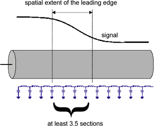
Tip
This suggests a very powerful rule of thumb: For an adequate bandwidth of the n-section lumped-circuit model at the given rise time, RT (in nsec), the size (in inches) of each LC section should be no longer than 1.7 × RT inches.
If the rise time is 1 nsec, the length of each single LC should be less than 1.7 inches. If the rise time is 0.5 nsec, the length of each LC section should be no longer than 0.5 × 1.7 = 0.85 inches.
Tip
Of course, an ideal, distributed transmission line model is always a good model for a uniform interconnect, at low frequency and at high frequency.
7.19 Frequency Variation of the Characteristic Impedance
So far, we have been assuming the characteristic impedance of a transmission line is constant with frequency. As we have seen, the input impedance, looking into the front of a transmission line, is strongly frequency dependent. Does the characteristic impedance vary with frequency? In this section, we are assuming the transmission line is lossless. In a later chapter, we will look at the case where the transmission line has loss. We will see that the characteristic impedance does vary slightly due to the losses.
As we have seen, the characteristic impedance of an ideal lossless transmission line is related to the capacitance and inductance per length as:
![]()
Providing the dielectric constant of the interconnect is constant with frequency, the capacitance per length will be constant. This is a reasonable assumption for most materials, though in some cases, the dielectric constant will vary slightly.
As we saw in the last chapter, the loop inductance per length of a line will vary with frequency due to skin-depth effects. In fact, the loop inductance will start out higher at low frequency and decrease as all the currents distribute to the outer surface. This would suggest that characteristic impedance will start out higher at low frequency and decrease to a constant value at higher frequency.
At frequencies well above the skin depth, we would expect all the currents to be on the outer surface of all the conductors and not to vary with frequency beyond this point. The loop inductance should be constant and the characteristic impedance should be constant. We can estimate this frequency for a 1-ounce copper conductor. The skin depth for copper is about 20 microns at 10 MHz. The thickness of 1-ounce copper is about 34 microns. We would expect to see the characteristic impedance start to decrease around 1 MHz to 10 MHz and stop decreasing at about 100 MHz, where the skin depth is only 6 microns.
We can calculate the frequency dependence of the characteristic impedance for a 50-Ohm microstrip with 1-ounce copper traces using a 2D field solver. The result is shown in Figure 7-43.
Figure 7-43 Calculated frequency variation of the characteristic impedance due to skin-depth effects, for a 50-Ohm line in FR4 with 1-ounce copper traces. Calculated with Ansoft’s 2D Extractor.
This shows that at low frequency, the characteristic impedance is high, starts dropping at about 1 MHz, and continues to drop until about 50 MHz. The total drop from DC to high frequency is about 7 Ohms, or less than 15%.
Tip
Above about 50 MHz, the characteristic impedance of a transmission line is constant with frequency. This is the “high-frequency” characteristic impedance and is the value typically used for all evaluation of the behavior of high-speed signals.
7.20 The Bottom Line
1. A transmission line is a fundamentally new ideal-circuit element that accurately describes all the electrical properties of a uniform cross-sectional interconnect.
2. Forget the word ground. Think return path.
3. Signals propagate down a transmission line at the speed of light in the material surrounding the conductors. This primarily depends on the dielectric constant of the insulation.
4. The characteristic impedance of a transmission line describes the instantaneous impedance a signal would see as it propagates down the line. It is independent of the length of the line.
5. The characteristic impedance of a line primarily depends inversely on the capacitance per length and the speed of the signal.
6. The input impedance looking into the front end of a transmission line changes with time. It is initially the characteristic impedance of the line during the round-trip time of flight, but can end up being anything depending on the termination, the length of the line, and how long we measure the impedance.
7. A controlled-impedance board has all its traces fabricated with the same characteristic impedance. This is essential for good signal integrity.
8. A signal propagates through a transmission line as a current loop with the current going down the signal path and looping back through the return path. Anything that disturbs the return path will increase the impedance of the return path and create a ground-bounce voltage noise.
9. An ideal transmission line can be approximated with an n-section LC lumped-circuit model. The higher the bandwidth required, the more LC sections required.
10. For good accuracy, there should be at least 3.5 LC sections along the spatial extent of the leading edge.
11. An ideal transmission line is always a good model for a uniform interconnect, independent of the rise time and interconnect length.