CHAPTER 3
Discrete Transistor Circuitry
This chapter deals with small-signal design using discrete transistors, specifically BJTs. Many things found in standard textbooks are skated over quickly. It concentrates on audio issues and gives information that I do not think appears anywhere else, including the distortion behaviour of various configurations.
Why Use Discrete Transistor Circuitry?
Circuitry made with discrete transistors is not obsolete. It is appropriate when:
- A load must be driven to higher voltages than an opamp can sustain between the supply rails. Opamps are mostly restricted to supply voltages of +/-18 or +/-20 volts. Hybrid-construction amplifiers, typically packaged in TO3 cans, will operate from rails as high as +/-100 V, but they are very expensive and not optimised for audio use in parameters like crossover distortion. Discrete circuitry provides a viable alternative, but it must never be forgotten that excessive output signal levels may damage opamp equipment. Hi-fi is very rarely equipped with input voltage protection.
- A load requires more drive current, because of its low impedance, than an opamp can provide without overheating or current limiting; e.g. any audio power amplifier.
- The best possible noise performance is required. Discrete bipolar transistors can outperform opamps, particularly with low source resistances, say 500 Ω or less. The commonest examples are moving-coil head amps and microphone preamplifiers. These almost invariably use a discrete input device or devices, with the open-loop gain (for linearity) and load-driving capability provided by an opamp that may itself have fairly humble noise specs.
- The best possible distortion performance is demanded. Most opamps have Class-B or -AB output stages, and many of them (though certainly not all) show clear crossover artefacts on the distortion residual. A discrete opamp can dissipate more power than an IC, and so can have a Class-A output stage, sidestepping the crossover problem completely.
- When it would be necessary to provide a low-voltage supply to run just one or two opamps. The cost of extra transformer windings, rectifiers, reservoirs, and regulators will buy a lot of discrete transistors. For example, if you need a buffer stage to drive a power amplifier from a low impedance, it may be more economical and save space and weight to use a discrete emitter-follower running from the same rails as the power amplifier. In these days of auto-insertion, fitting the extra parts on the PCB will cost very little.
- Purely for marketing purposes, as you think you can mine a vein of customers that don’t trust opamps.
When studying the higher reaches of discrete design, the most fruitful source of information is paradoxically papers on analogue IC design. This applies with particular force to design with BJTs. The circuitry used in ICs can rarely be directly adapted for use with discrete semiconductors, because some features such as multiple collector transistors and differing emitter areas simply do not exist in the discrete transistor world; it is the basic principles of circuit operation that can be useful. A good example is a paper by Erdi, dealing with a unity-gain buffer with a slew rate of 300 V/μs [1]. Another highly informative discourse is by Barry Hilton [2], which also deals with a unity-gain buffer.
A little caution is required when a discrete stage may be driving not another of its own kind on the same supply rail but opamp-based circuitry that is likely to be running off no more than ±18 V, as peak signal levels may drive the opamp inputs outside their rail voltages and cause damage. This normally only applies to discrete output stages but should be kept in mind whenever the supply rail is higher than +36 V for single rail and ±18 V for dual rail.
Bipolars and FETs
This chapter only deals with bipolar transistors. Their high transconductance and predictable operation make them far more versatile than FETs. The highly variable Vgs of an FET can be dealt with by expedients such as current-source biasing, but the low transconductance, which means low feedback and poor linearity, remains a problem. FETs have their uses when super-high input impedances are required, and an example of a JFET working with an opamp that provides loop gain can be found in Chapter 17 on microphone amplifiers.
Bipolar Junction Transistors
There is one thing to get straight first:
THE BIPOLAR JUNCTION TRANSISTOR IS A VOLTAGE-OPERATED DEVICE.
What counts is the base-emitter voltage, or Vbe. Certainly a BJT needs base current to flow for it to operate, but this is really an annoying imperfection rather than the basis of operation. I appreciate this may take some digesting; far too many discussions of transistor action say something like “a small current flowing into the base controls a much larger current flowing into the collector”. In fact, the only truly current-operated amplifying device that comes to mind is the Hall-effect multiplier, and you don’t come across those every day. I’ve certainly never seen one used in audio –could be a market niche there.
Transistor operation is thus: if the base is open-circuit, then no collector current flows, as the collector-base junction is effectively a reverse-biased diode, as seen in Figure 3.1. There is a little leakage through from the collector to the emitter, but with modern silicon BJTs, you can usually ignore it.
When the base is forward biased by taking it about 600 mV above the emitter, charge carriers are launched into the base region. Since the base region is narrow, the vast majority shoot through into the collector to form the collector current Ic. Only a small proportion of these carriers is snared in the base and become the base current Ib, which is clearly a result and not the cause of the base-emitter voltage. Ib is normally just a nuisance.

Figure 3.1 Current flow through a bipolar transistor and the fundamental transistor equation.
The Transistor Equation
Every bipolar transistor obeys the Ebers-Moll transistor equation shown in Figure 3.1 with startling accuracy over 9 or 10 decades of Ic, which is a pretty broad hint that we are looking at the fundamental mechanism. In contrast, beta varies with Ic, temperature, and just about everything else you can think of. The collector current is to a first approximation independent of collector voltage –in other words, it is a current-source output. The qualifications to this are:
- This only holds for Vce above, say, 2 volts.
- It is not a perfect current-source; even with a high Vce, Ic increases slowly with Vce. This is called the Early Effect, after Jim Early [3], and has nothing to do with timing or punctuality. It is a major consideration in the design of stages with high voltage gain. The same effect when the transistor is operated in reverse mode –a perversion that will not concern us here –has sometimes been called the Late Effect. Ho-ho.
Beta
Beta (or hfe) is the ratio of the base current Ib to the collector current Ic. It is not a fundamental property of a BJT. Never design circuits that depend on beta, unless of course you’re making a transistor tester.
Here are some of the factors that affect beta. This should convince you that it is a shifty and thoroughly untrustworthy parameter:
- Beta varies with Ic. First it rises as Ic increases, reaching a broad peak, then it falls off as Ic continues to increase.
- Beta increases with temperature. This seems to be relatively little known. Most things, like leakage currents, get worse as temperature increases, so this makes a nice change.
- Beta is lower for high-current transistor types.
- Beta is lower for high-Vceo transistor types. This is a major consideration when you are designing the small-signal stages of power amplifiers with high supply rails.
- Beta varies widely between nominally identical examples of the same transistor type.
A very good refutation of the beta-centric view of BJTs is given by Barrie Gilbert in [4].
Unity-Gain Buffer Stages
A buffer stage is used to isolate two portions of circuitry from each other. It has a high input impedance and low output impedance; typically it prevents things downstream from loading things upstream. The use of the word “buffer” normally implies “unity-gain buffer”, because otherwise we would be talking about an amplifier or gain stage. The gain with the simpler discrete implementations is in fact slightly less than one. The simplest discrete buffer circuit-block is the one-transistor emitter-follower; it is less than ideal both in its mediocre linearity and its asymmetrical load-driving capabilities. If we permit ourselves another transistor, the complementary feedback-pair (CFP) configuration gives better linearity. Both versions can have their load-driving performance much improved by replacing the emitter resistor with a constant-current source or a push-pull Class-A output arrangement.
If the CFP stage is not sufficiently linear, the next stage in sophistication is to combine an input differential pair with an output emitter-follower using three transistors. This arrangement, often called the Schlotzaur configuration [5], can be elaborated until it gives a truly excellent distortion performance. Its load-driving capability can be enhanced in the same way as the simpler configurations.
The Simple Emitter-Follower
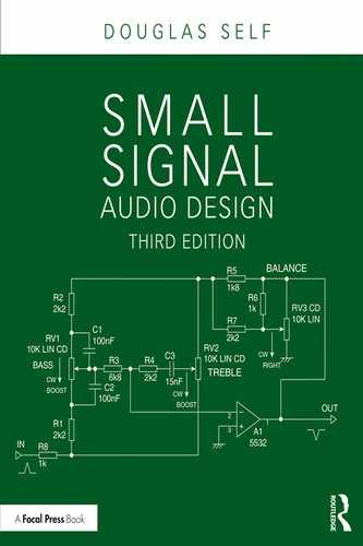
The simplest discrete circuit-block is the one-transistor emitter-follower. This count of one does not include extra transistors used as current sources, etc., to improve load-driving ability. It does not have a gain of exactly unity, but it is usually pretty close.
Figure 3.2 shows a simple emitter-follower with a 2k7 emitter resistor Re, giving a quiescent current of 8.8 mA with ±24 V supply rails. Biasing is by a high-value resistor R1 connected to 0 V. Note the polarity of the output capacitor; the output will sit at about -0.6 V due to the Vbe drop, plus a little lower due to the voltage drop caused by the base current Ib flowing through R1.
The input impedance is approximately that of the emitter resistor in parallel with an external loading on the stage multiplied by the transistor beta:
Don’t expect the output impedance to be as low as an opamp with plenty of NFB. The output impedance is approximately that of the source resistance divided by beta:
- where Rs is the source impedance.
The gain of an emitter-follower is always slightly less than unity, because of the finite transconductance of the transistor. Essentially the intrinsic emitter resistance re (not be confused with the physical component Re) forms a potential divider with the output load. It is simple to work out the small-signal gain at a given operating point. The value of re is given by 25/Ic (for Ic in mA). Since the value of re is inversely proportional to Ic, it varies with large signals, and it is one cause of the rather imperfect linearity of the simple emitter-follower. Heavier external loading increases the modulation of Ic, increases the gain variation, and so increases distortion.
Figure 3.2 The simple emitter-follower circuit running from ±24 V supply rails.
Figure 3.2 shows the emitter-follower with an AC-coupled load. Its load-driving capability is not very good. While the transistor can, within limits, source as much current as required into the load, the current-sinking ability is limited by the emitter resistor R2, which forms a potential divider with the load resistance Rload. With the values shown here, negative clipping occurs at about -10 V, severely limiting the maximum output amplitude. The circuit shows a high-voltage low-beta transistor type running from ±24 V rails to give worst-case performance results and to exploit the ability of discrete circuitry to run from high-voltage rails.
The simple emitter-follower has several factors that affect its distortion performance:
- Distortion is reduced as the emitter resistor is reduced for a given load impedance.
- Distortion is reduced as the DC bias level is raised above the midpoint.
- Distortion increases as the load impedance is reduced.
- Distortion increases monotonically with output level.
- Distortion does NOT vary with the beta of the transistor. This statement assumes low-impedance drive, which may not be the case for an emitter-follower used as a buffer. If the source impedance is significant, then beta is likely to have a complicated effect on linearity –and not always for the worse.
Emitter-follower distortion is mainly second harmonic, except when closely approaching clipping. This is entirely predictable, as the circuit is asymmetrical. Only symmetrical configurations, such as the differential pair, restrict themselves to generating just odd harmonics, and then only when they are carefully balanced. [6] Symmetry is often praised as desirable in an audio circuit, but this is subject to Gershwin’s Law: “It ain’t necessarily so”. Linearity is what we want in a circuit, and symmetry is not necessarily the best way to get it.

Figure 3.3 How various external loads degrade the linearity of the simple emitter-follower. Re = 2k7.
Because the distortion is mostly second harmonic, its level is proportional to amplitude, as seen in Figure 3.3. At 2 Vrms with no load, it is about 0.006%, rising to 0.013% at 4 Vrms. External loading always makes the distortion worse, and more rapidly as the amplitude approaches the clipping point; the THD is more than doubled from 0.021% to 0.050% at 6 Vrms, just by adding a light 6k8 load. For these tests, Re was 2k7, as in Figure 3.2. For both the EF and CFP circuits, distortion is flat across the audio band, so no THD/frequency plots are given.
Insight into what’s happening can be gained by using SPICE to plot the incremental gain over the output swing, as in Figure 3.4. As loading increases, the curvature of the gain characteristic becomes greater for a given voltage swing. It is obvious that the circuit is much more linear on the positive side of 0 V, explaining why emitter-followers give less distortion when biased above the midpoint. This trick can be very useful if the full output swing is not required.

Most amplifier stages are biased so the quiescent output voltage is at the midpoint of the operating region to allow the maximum symmetrical voltage swing. However, the asymmetry of the simple emitter-follower’s output current-capability means that if there is significant loading, a greater symmetrical output swing is often possible if the stage is biased positive of 0 V.
If the output is loaded with 2k2, negative clipping occurs at -8 V, which allows a maximum output amplitude of only 5.6 Vrms. The unloaded output capability is about 12 Vrms. If the bias point is raised from 0 V to +5 V, the output capability becomes roughly symmetrical, and the maximum loaded output amplitude is increased to 9.2 Vrms. Don’t forget to turn the output capacitor around.
The measured noise output of this stage with a 40 Ω source resistance is a commendably low -122.7 dBu (22–22 kHz) but with a base-stopper resistor (see what follows) of 1 kΩ this degrades to -116.9 dBu. A higher stopper of 2k7 gives -110.4 dBu.
The Constant-Current Emitter-Follower
The simple emitter-follower can be greatly improved by replacing the sink resistor Re with a constant-current source, as shown in Figure 3.5. The voltage across a current-source does not (to a good approximation) affect the current through it, so if the sink current is large enough, a load can be driven to the full voltage swing in both directions.

Figure 3.5 Emitter-follower with a constant-current source replacing the emitter resistor.
The current source Q2 is biased by D1, D2, with the 22 kΩ resistor R3 powering the diodes. One diode cancels the Vbe drop of Q2, while the other sets up 0.6 V across the 100 Ω resistor R2, establishing the quiescent current at 6 mA. This simple bias system works quite adequately if the supply rails are regulated but might require filtering if they are not. The 22 kΩ value is non-critical; so long as the diode current exceeds the Ib of Q2 by a reasonable factor (say 10 times), there will be no problem.
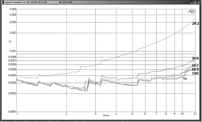
Figure 3.6 shows that distortion is much reduced. With no external load, the 0.013% of the simple emitter-follower (at 4 Vrms) has become less than 0.0003%, the measurement system noise floor. This is because the amount by which the Q1 collector current is modulated is very much less. The linearity of this emitter-follower is still degraded by increasing loading, but to a much lesser extent; with a significant external load of 4k7, the 0.036% of the simple emitter-follower (at 4 Vrms) becomes 0.006%. The steps in the bottom (no-load) trace are artefacts of the AP SYS-2702 measuring system.

The noise performance of this stage is exactly as for the simple emitter-follower.
The Push-Pull Emitter-Follower
This is an extremely useful and trouble-free form of push-pull output; I have used it many times in preamplifiers, mixers, etc. I derived the notion from the valve-technology White cathode-follower, described by Nelson-Jones in a long-ago Wireless World. [7] The original reference is a British Patent taken out by Eric White in 1940. [8]

Figure 3.7 Circuit of push-pull emitter-follower. Quiescent current still 6 mA as before, but the load-driving capability is twice as great.
Figure 3.7 shows a push-pull emitter-follower. When the output is sourcing current, there is a voltage drop through the upper sensing resistor R5, so its lower end goes downwards in voltage. This is coupled to the current-source Q2 through C3 and tends to turn it off. Likewise, when the current through Q1 falls, Q2 is turned on more. This is essentially a negative-feedback loop with an open-loop gain of unity, and so by simple arithmetic, the current variations in Q1, Q2 are halved, and this stage can sink twice the current of the constant-current version described earlier while running at the same quiescent current. The effect of loading on linearity is once again considerably reduced, and only one resistor and one capacitor have been added.
This configuration needs fairly clean supply rails to work, as any upper-rail ripple or disturbance is passed directly through C3 to the current source, modulating the quiescent current and disrupting the operation of the circuit.
Push-pull action further improves the linearity of load driving; the THD with a 4k7 external load is halved from 0.006% for the constant-current version (4 Vrms) to 0.003% at the same quiescent current of 6 mA, as seen in Figure 3.8. This is pretty good linearity for such simple circuitry.

Figure 3.8 How loading degrades linearity of the push-pull emitter-follower. Loads from 10 kΩ to 2k2. Quiescent current 6 mA.
Emitter-Follower Stability
The emitter-follower is about as simple as an amplifier gets, and it seems highly unlikely that it could suffer from obscure stability problems. However, it can and often does. Emitter-followers are liable to RF oscillation when fed from an inductive source impedance. This oscillation is in the VHF region, usually in the area 100–400 MHz, and will be quite invisible on the average oscilloscope; however, a sure sign of this problem is unusually high distortion that varies strongly when the transistor is touched with a probing finger. One way to stop this is to put a “base-stopper” resistor directly in series with the base. This should come after the bias resistor to prevent loss of gain. Depending on the circuit conditions, the resistor may be as low as 100 Ω or as high as 2k7. The latter generates -119.6 dBu of Johnson noise, which in itself is inconvenient in low-noise circuitry, but the effects of the transistor noise current flowing through it are likely to be even worse. Base-stopper resistors are not shown in the following diagrams to aid clarity, but you should always be aware of the possible need for them. This also applies to the CFP configuration, which is equally, if not more, susceptible to the problem.
The instability is due to the fact that the typical emitter-follower is fed from a source with some inductance and has some capacitive loading, even if it is only due to stray capacitance, as in Figure 3.9a, where the transistor internal base-emitter capacitance Cbe is included. If this is redrawn as in Figure 3.9b, it is the classic circuit of a Colpitts oscillator. For more information on this phenomenon, see Feucht [9] and de Lange. [10]

Figure 3.9 Emitter-follower oscillation: the effective circuit at a) bears a startling resemblance to the Colpitts oscillator at b).
CFP Emitter-Followers
The simple emitter-follower is lacking both in linearity and load-driving ability. The first shortcoming can be addressed by adding a second transistor to increase the negative feedback factor by increasing the open-loop-gain. This also allows the stage to be configured to give voltage gain, as the output and feedback point are no longer inherently the same. This arrangement is usually called the complementary feedback pair (hereafter CFP) though it is sometimes known as the Szilaki configuration. This circuit can be modified for constant-current or push-pull operation exactly as for the simple emitter-follower.

Figure 3.10 The CFP emitter-follower. The single transistor is replaced by a pair with 100% voltage feedback to the emitter of the first transistor.
Figure 3.10 shows an example. The emitter resistor Re is the same value as in the simple emitter-follower to allow meaningful comparisons. The value of R4 is crucial to good linearity, as it sets the Ic of the first transistor. The value of 3k3 shown here is a good compromise.
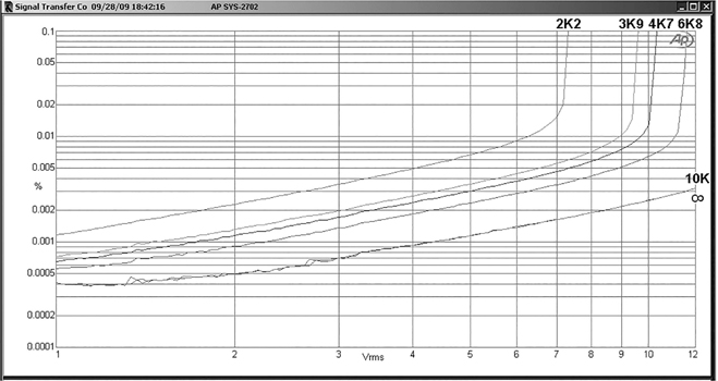
Figure 3.11 How loading affects the distortion of a CFP emitter-follower. THD at 6 Vrms, 6k8 load is only 0.003% compared with 0.05% for the simple EF. Re is 2K7.
This circuit is also susceptible to emitter-follower oscillation, particularly if it sees some load capacitance, and will probably need a basestopper. If 1 kΩ does not do the job, try adding a series output resistor of 100 Ω close to the stage to isolate it from load capacitance.
Figure 3.11 shows the improved linearity; Figure 3.12 is the corresponding SPICE simulation; the measured noise output with a 100 Ω base-stopper is -116.1 dBu.
If we replace Re with a 6 mA current-source, as in Figure 3.13, we once more get improved linearity and load-driving capability, as shown in Figure 3.14. The 6 Vrms, 6k8 THD is now only just above the noise at 0.0005%. (Yes, three zeros after the point: three-transistor circuitry can be rather effective.)
Converting the constant-current CFP to push-pull operation as in Figure 3.15 gives another improvement in linearity and load driving. Figure 3.16 shows that now only the results for 2k2 and 3k9 loading are above the measurement floor.

Figure 3.12 SPICE simulation of the CFP circuit in Figure 3.10 for different load resistances. The curves are much flatter than those in Figure 3.4, even though the vertical scale has been expanded.
Improved Unity-Gain Buffers
There is often a need for a unity-gain buffer with very low distortion. If neither the simple emitter-follower, made with one transistor, nor the CFP configuration with two transistors is adequately linear, we might ponder the advantages of adding a third transistor to improve performance, without going to the complexity of the discrete opamps described later in this chapter. (In our transistor count, we are ignoring current-sources used to create the active output loads that so improve linearity into significant external loading.)
One promising next step is a three-transistor configuration that is often called the Schlotzaur configuration; see Feucht [5] and Staric and Margan. [11] The single input transistor in the CFP emitter-follower is now replaced with a long-tail pair with 100% feedback to Q1, as in Figure 3.17a. Because LTPs have the property of cancelling out their even-order distortion [6], you might expect a considerable improvement. You would be wrong; running on ±15 V rails, we get 0.014% at 6 Vrms unloaded, almost flat across the audio band. The linearity is much inferior to the CFP emitter-follower. The open-loop gain, determined by measuring the error voltage between Q1, Q2 bases, is 249 times.

Figure 3.13 Constant-current CFP follower. Once more, the resistive emitter load is replaced by a constant-current source to improve current sinking.

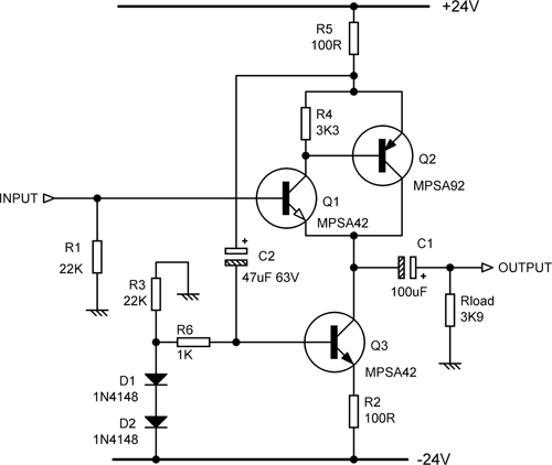
Figure 3.15 Circuit of a push-pull CFP follower. This version once more gives twice the load-driving capability for no increase in standing current.
It’s not a promising start, but we will persist! Replace the collector load R2 with a current source of half the value of the tail current source as in Figure 3.17b, and the linearity is transformed, yielding 0.00075% at 6 Vrms unloaded on ±15 V rails. Increasing the rails to ±18 V gives 0.00066% at 6 Vrms, and a further increase to ±24 V, as high-voltage operation is part of what discrete design is all about, gives 0.00042% at 6 Vrms (unloaded). It’s the increase in the positive rail that gives the improvement. Reducing the measurement bandwidth from 80 kHz to 22 kHz for a 1 kHz signal eliminates some noise and gives a truer figure of 0.00032% at 6 Vrms. The open-loop gain is increased to 3400 times.
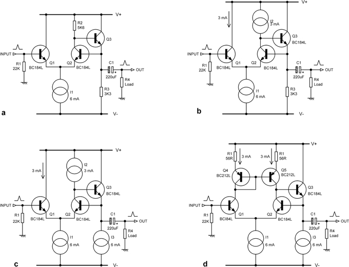
Adding loading to the buffer actually has very little effect on the linearity, but its output capability is clearly limited by the use of R3 to sink current, just as for a simple emitter-follower. Replacing R3 with a 6 mA constant-current source, as for previous circuits, much improves drive capability and also improves linearity somewhat. See Figure 3.17c. On ±30 V rails, we get a reading of 0.00019% at 5 Vrms with a 2k2 load, and that is mostly the noise in a 22 kHz bandwidth.

Finally, we remove current source I2 and replace it with a simple current mirror in the input pair collectors, as in Figure 3.17d, in the pious hope that the open-loop gain will be doubled and distortion halved. On ±30 V rails, there is a drop in THD from 0.00019% to 0.00017% at 5 Vrms with a 2k2 load (22 kHz bandwidth), but that is almost all noise, and I am pushing the limits of even the magnificent Audio Precision SYS-2702. This goes to show that there are other ways of designing low-distortion circuitry apart from hefting a bucket of opamps.
Figure 3.18 shows the distortion plot at 5 Vrms. Using an 80 kHz bandwidth so the HF end is meaningful means the readings are higher and virtually all noise below 10 kHz. It also gives another illustration of the distortion generated by under-sized coupling capacitors. C1 started as 22 μF, but you can see that 220 μF is required to suppress distortion at 10 Hz with a 2k2 load, and 470 μF might be better.
SPICE analysis shows that the collector currents of the input pair Q1, Q2 are somewhat unbalanced by the familiar base-current errors of a simple current mirror. Replacing the simple current mirror with the well-known Wilson improved mirror might get us further improvement – if we could measure it. Work in progress…
The circuit we have now could still be regarded as a much-enhanced emitter-follower, but it is probably more realistic to consider it as a two-stage discrete opamp, as it could be configured to give a closed loop of greater than unity.
Gain Stages
This section covers any discrete transistor stage that can give voltage gain. It may be as simple as a single transistor or as complex as an opamp implemented with discrete components. A single transistor can give voltage gain in either series or shunt mode.
One-Transistor Shunt-Feedback Gain Stages
Single-transistor shunt-feedback gain stages are inherently inverting and of very poor linearity by modern standards. The circuit in Figure 3.19 is inevitably a collection of compromises. The collector resistor R4 should be high in value to maximise the open-loop gain; but this reduces the collector current of Q1 and thus its transconductance and hence reduces open-loop gain once more. The collector resistor must also be reasonably low in value, as the collector must drive external loads directly. Resistor R2, in conjunction with R3, sets the operating conditions. This stage has only a modest amount of shunt feedback via R3, and Q1 base can hardly be called a virtual earth. However, such circuits were once very common in low-end discrete preamplifiers, back in the days when the cost of an active device was a serious matter. Such stages are still occasionally found doing humble jobs like driving VU meters, but the cost advantage over anopamp section is small if it exists at all.

Figure 3.19 Circuit of single-transistor gain stage, shunt-feedback version. +24 V rail.
The gain of the stage in Figure 3.19 is at a first look 220k/68k = 3.23 times, but the actual gain is 2.3x (with no load) due to the small amount of open-loop gain available. The mediocre distortion performance that must be expected even with this low gain is shown in Figure 3.20.
One-Transistor Series-Feedback Gain Stages
Single-transistor series-feedback gain stages are made by creating a common-emitter amplifier with a feedback resistor that gives series voltage feedback to the emitter. The gain is the ratio of the collector and emitter resistors if loading is negligible. Note that unlike opamp-based series-feedback stages, this one is inherently inverting. To make a non-inverting stage with a gain more than unity requires at least two transistors because of the inversion in a single common-emitter stage.
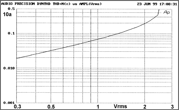
Figure 3.20 Single-transistor shunt-feedback gain stage, distortion versus level. +24 V rail. Gain is 2.3 times.
This very simple stage, shown in Figure 3.21, naturally has disadvantages. The output impedance is high, being essentially the value of the collector resistor R3. The output is not good at either sinking or sourcing current.
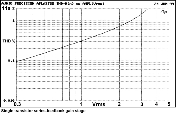
The distortion performance as seen in Figure 3.22 is indifferent, giving 0.3% THD at 1 Vrms out. Compare this with the shunt-feedback one-transistor gain stage, which gives 0.07% under similar conditions.

Figure 3.21 Circuit of single-transistor series-feedback gain stage. +24 V rail.
Two-Transistor Shunt-Feedback Gain Stages

Figure 3.23 Two-transistor gain stage with shunt-feedback. +24 V rail. Gain is three.
Before the advent of the opamp, inverting stages were required for tone controls and virtual-earth summing amplifiers. The one-transistor amplifier stage already described is deficient in distortion and load-driving capability. A much better amplifier can be made with two transistors, as in Figure 3.23. The voltage gain is generated by Q1, which has a much higher collector resistor R4 and so much higher gain. This is possible because Q2 buffers it from external loading and allows a higher NFB factor. See Figure 3.24 for the distortion performance.

With the addition of bootstrapping, as shown in Figure 3.25, the two-transistor stage has its performance transformed. Figure 3.26 shows how THD is reduced by a factor of 10; 0.15% at 1 Vrms in, 3 Vrms out becomes 0.015%, which is much more respectable. The improvement is due to the increased voltage-gain of the first stage giving a higher NFB factor. THD is still approximately proportional to level, as the distortion products are mainly second harmonic. Clipping occurs abruptly at 2.9 Vrms in, 8.7 Vrms out; abrupt clipping onset is characteristic of stages with a high NFB factor. Stages like this were commonly used as virtual-earth summing amplifiers in mixing consoles before acceptable opamps were available at reasonable cost.
Figure 3.27 shows that the distortion is further reduced to 0.002% at 3 Vrms out if the impedance of the input and feedback networks is reduced by 10 times. SPICE simulation confirms that this is because the signal currents flowing in R1 and R5 are now larger compared with the non-linear currents drawn by the base of Q1. There is also a noise advantage.

Figure 3.25 Two-transistor shunt-feedback stage, with bootstrapping added to the first stage to improve linearity. Q1 collector current is 112 μA. +24 V rail.


Figure 3.27 The distortion is reduced by a further factor of at least five if the impedance of the input and feedback networks is reduced by 10 times. +24 V rail. Output 3 Vrms.

Figure 3.28 shows how output drive capability can be increased, as before, by replacing R6 with a 6 mA current source. The input and feedback resistors R1, R5 have again been scaled down by a factor of 10. Push-pull operation can also be simply implemented as before. The EIN of this version is -116 dBu.
The constant-current and push-pull options can also be added to more complex discrete stages. Some good examples can be found in a preamplifier design of mine. [12]
Two-Transistor Shunt-Feedback Stages: Improving Linearity
As is usual with discrete configurations, the quickest way to improve linearity is to crank up the supply voltage if that is feasible. This obviously increases the power consumed by the circuitry, but this is not normally a major issue. Figure 3.29 shows the powerful effect of increasing the rail voltage on both the LF and HF distortion regimes. It is interesting to note that this simple configuration shows HF distortion (mainly second harmonic) increasing at 6 dB/octave with frequency, despite the simplicity of the circuit and the apparent absence of compensation capacitance. Open-loop gain does fall off at HF due to the internal Cbc of Q1, but the major source of HF distortion is the non-linear nature of this Cbc, which varies strongly in capacitance with the voltage across it. There is more on this vital point in the later section on discrete opamps.

Table 3.1 summarises how the distortion at 1 kHz drops quickly at first, as the supply voltage is increased, but the improvement slows down at higher voltages. The input was 1 Vrms and the output 3.23 Vrms. These measurements were all taken with the emitter-resistor R6 at 2k7, as shown in Figure 3.25. R1 was 6k8 and R5 was 22 kΩ, as for Figure 3.27 and Figure 3.28.
In this configuration, there are two stages, both of which have a certain curvature to their in/out characteristics. With discrete design, you have some control over both of them, and there is always the possibility that you might be able to reduce distortion by altering the curvatures so that some degree of cancellation occurs in the distortion produced by each stage. This will be most effective on second-harmonic distortion.
A convenient way to alter the curvature of the second stage is to vary the value of the emitter resistor R6 in Figure 3.25. The results of doing this are shown in Table 3.2; the input level was 1 Vrms and the output level 3.23 Vrms.
The second row shows the standard results, as obtained from Figure 3.25, with R6 set to 2k7. Our first experiment is to raise its value to 3k3, but this is clearly a step in the wrong direction, as THD increases from 0.00435% to 0.00466%. We therefore try reducing R6 to 2k2 and get an immediate improvement to 0.00378%. Pressing on further, we reduce R6 to 2k0, and THD falls again, but this time by a smaller amount, giving 0.00360%. It looks as if further decreases will yield diminishing benefits, and the increased standing-current in the emitter-follower may have serious consequences for power dissipation at higher supply voltages. Looking at the first four rows of the table, it is clear we get a useful improvement in distortion performance simply by changing one component value for no extra cost at all.
| Supply voltage | THD 1 kHz | THD reduction ratio ref +24 V |
|---|---|---|
| +24 V | 0.00435% | 1.00 |
| +30 V | 0.00324% | 0.74 |
| +36 V | 0.00262% | 0.60 |
| +40 V | 0.00228% | 0.52 |
| +45 V | 0.00201% | 0.46 |
| +48 V | 0.00188% | 0.43 |
| Supply voltage | R6 value | THD 1 kHz | THD reduction ratio |
|---|---|---|---|
| +24 V | 3k3 | 0.00466% | 1.09 |
| +24 V | 2k7 | 0.00435% | 1.00 (reference) |
| +24 V | 2k2 | 0.00378% | 0.88 |
| +24 V | 2k0 | 0.00360% | 0.84 |
| +30 V | 2k0 | 0.00287% | 0.67 |
| +36 V | 2k0 | 0.00228% | 0.53 |
| +40 V | 2k0 | 0.00204% | 0.48 |
| +45 V | 2k0 | 0.00179% | 0.42 |
| +48 V | 2k0 | 0.00167% | 0.39 |
Since it appears we have gone about as far as we can in tweaking the output emitter-follower, we can consider a more radical step. As a general rule, any emitter-follower in a discrete transistor configuration can be inverted –in other words, replaced by its complementary equivalent. This can be very useful when attempting to cancel the distortion from different stages, as just described. The result of this move is shown in Figure 3.30, where the output emitter-follower Q2 is now a PNP device.

Figure 3.30 Two-transistor shunt-feedback amplifier with the emitter-follower Q2 inverted. Note R1 and R5 have the reduced values.
Unfortunately, we discover when we do the measurements that we have royally messed up an existing distortion cancellation rather than improved it, as shown in Table 3.3. (The “THD ratio” is based on the original configuration; the second row of Table 3.2 is the reference.) The distortion with a +24 V supply rail is almost doubled, and clearly we are reinforcing the curvature of the two stages rather than partially cancelling it. Increasing the supply voltage still improves the linearity, as it almost always will.
| Supply voltage | THD 1 kHz | THD ratio |
|---|---|---|
| +24 | 0.00850% | 1.99 |
| +30 | 0.00711% | 1.66 |
| +36 | 0.00589% | 1.38 |
| +40 | 0.00521% | 1.22 |
| Supply voltage | R6 value | THD 1 kHz | THD ratio |
|---|---|---|---|
| +24 | 2K2 | 0.00882% | 2.06 |
| +24 | 2K7 | 0.00850% | 1.99 |
| +24 | 3K3 | 0.00806% | 1.89 |
We can again attempt to improve the linearity by modifying the value of the output emitter resistor R6, but it really doesn’t help very much. The deeply unimpressive results are seen in Table 3.4. The “THD ratio” reference is again the second row of Table 3.2.
Clearly in this case, the conventional configuration with two NPN transistors is the superior one. It was and is the most common version encountered, so sometimes conventional is optimal.
Two-Transistor Shunt-Feedback Stages: Noise
The noise output of the shunt-feedback circuit in Figure 3.28 with R1 = 6k8 and R5 = 22 kΩ is -99.5 dBu. To work out the equivalent input noise (EIN), we need to know the actual noise gain at which the circuit works, not the closed-loop gain. The latter is simply (R5/R1), but the apparent noise gain is higher at (R5/R1)+1, which evaluates as +12.5 dB, as it would be for the equivalent opamp circuit. The noise gain is actually rather higher still, because we must allow for the presence of the biasing resistor R2. This raises the true noise gain to +16.2 dB. In the typical application for this kind of circuit, that of virtual-earth summing amp, there would have been many input resistances R1, and the presence of R2 would have made relatively little difference to the overall noise performance.
Armed with the true noise gain, we can work out the EIN as -115.7 dBu, which is basically the noise performance of the first stage, as it implements all the voltage gain. It has to be said that I have so far made no attempt to optimise the noise performance of the circuit shown here. Increasing the first-stage collector current would probably reduce the noise with the feedback values shown.
Two-Transistor Shunt-Feedback Stages: Bootstrapping
Choosing the right size for a bootstrap capacitor is not quite as straightforward as it appears. It looks as if quite a small value could be used because of the high impedance of the Q1 collector load. In Figures 3.25 and 3.28, the bootstrap capacitor C4 effectively sees only the 47 kΩ impedance of R8 to the supply rail, and a 2u2 capacitor in conjunction with this gives -3 dB frequency of 1.54 Hz, which looks ample.
But it is not. Figure 3.31 shows that this value gives an enormous rise in LF distortion, reaching 0.020% at 10 Hz. The reason for this steep rise is that bootstrapping as a means of gain enhancement requires the bootstrapped point to accurately follow the output of the voltage stage, because even small deviations from unity-gain in the bootstrapping mean that the increase in Q1 collector impedance, and hence the overall open-loop gain, is seriously compromised. Note that there is no requirement for R4 and R8 to be the same value, but their sum, in conjunction with the voltage conditions, will define Q1 collector current. Figure 3.31 also shows that a 47 μF bootstrap capacitor is big enough to keep the distortion flat down to 10 Hz, and going to 100 μF gives no further improvement.

We saw earlier that inverting the output emitter-follower made the distortion worse rather than better. There is, however, an interesting consequence of that inversion. We can now use what might be called DC bootstrapping, because no capacitor is used. The collector load of Q1 is a single resistor R4, and it is now connected between the base and emitter of the output emitter-follower Q2, as shown in Figure 3.32.
This technique eliminates the bootstrap capacitor and its potential problems but unfortunately is less linear. The distortion performance is summarised in Table 3.5, where once more, the “THD ratio” is based on the second row of Table 3.2 as the reference.

Figure 3.32 Two-transistor shunt-feedback amplifier with emitter-follower Q2 inverted and DC bootstrapping of the Q1 load R4.
| Supply voltage | R4 value | R6 value | THD 1 kHz | THD ratio |
|---|---|---|---|---|
| +24 | 6k8 | 2k7 | 0.00694% | 1.62 |
| +24 | 6k8 | 3k3 | 0.00705% | 1.65 |
| +24 | 6k8 | 2k2 | 0.00686% | 1.61 |
| +24 | 4k7 | 2k7 | 0.014% | 3.28 |
| +24 | 10k | 2k7 | 0.015% | 3.51 |
This configuration has better linearity than the inverted emitter-follower with capacitive bootstrapping, but it is still markedly worse than the original version of Figure 3.25. As Table 3.5 shows, tweaking R6 doesn’t help much. We can also try changing the value of the Q1 collector load R4, as it determines the Q1 collector current and is likely to have an important effect on circuit operation, but as the last two rows of Table 3.5 demonstrate, sadly we find that either increasing or decreasing it from 6k8 makes things a lot worse.
We have, however, saved two components –in particular an electrolytic capacitor has been eliminated, and these are the least reliable parts in the longterm due to their tendency to dry out and drop in value.

Figure 3.33 The bus residual for non-bootstrapped, capacitor-bootstrapped, and DC-bootstrapped two-transistor summing amplifiers. Measured relative to output voltage.
Two-Transistor Shunt-Feedback Stages as Summing Amplifiers
Two-transistor shunt-feedback stages like those described were used as virtual-earth summing amplifiers in mixers for many years. They were still in use in the early 1980s in mixer designs that were all discrete to avoid the compromises in noise and distortion that came with the (affordable) opamps of the day. A two-transistor summing amplifier is simply the design of Figure 3.25, with a 22 kΩ feedback resistor R5, the 6k8 input resistor R1 representing a summing resistor from a mixer channel. The junction of the two was the virtual-earth bus.
We have seen that the distortion of the two-transistor configuration is not stunning by modern standards, though it can be improved. Another important parameter for a summing amplifier is the level of the bus residual, which is the signal voltage actually existing on the virtual-earth bus. Ideally, this would be zero, but in the real world, it is non-zero because the summing amplifier has a finite open-loop gain. In simpler mixers, this can have serious effects on inter-bus crosstalk; this is discussed in more detail in Chapter 22.
Figure 3.33 shows the bus residual, relative to the summing amplifier output voltage, for three versions of the two-transistor configuration. With no bootstrapping, as in Figure 3.23, the bus residual is an unimpressive -52 dB. Adding conventional capacitor (AC) bootstrapping to increase the open-loop gain gives a much lower -66 dB, and DC bootstrapping, as described in the previous section, gives us -64 dB, indicating it is slightly less effective at raising the open-loop gain. This is probably because DC bootstrapping falls further short of unity-gain than AC bootstrapping. These two traces show a rise at the HF end which does not appear on the -52 dB trace; this is almost certainly due to the open-loop gain falling off at HF due to the Cbc of Q1. There is also a rise in bus residual at the LF end, looking the same for all three cases. I suspect increasing C2 would remove that.
Two-Transistor Series-Feedback Gain Stages
The circuit in Figure 3.34 clearly has a close family relationship with the CFP emitter-follower, which is simply one of these stages configured for unity gain. The crucial difference here is that the output is separated from the input emitter, so the closed-loop gain is set by the R3-R2 divider ratio.

Figure 3.34 Two-transistor gain stage, series-feedback. +24 V rail. Gain once more approximately three.

Figure 3.35 Two-transistor series-feedback stage. THD varies strongly with value of R4. +24 V rail.
Only limited NFB is available, so closed-loop gains of two or three times are usually the limit.
It is less easy to adapt this circuit to improve load-driving capability, because the feedback-resistive divider must be retained. Figure 3.35 shows that distortion performance depends strongly on the value of R4, the collector load for Q1. The optimal value for linearity and noise performance is around 4k7.
Discrete Opamp Design
When the previously described circuits do not show enough linearity or precision for the job in hand, or a true differential input is required, it may be time to use an opamp made from discrete transistors. The DC precision will be much inferior to an IC opamp and the parts count high compared with the other discrete configurations we have looked at, but the noise and distortion performance can both be very good indeed. A good example of discrete opamp usage is a preamplifier I designed a while back [13], though it must be said the opamps there could definitely be improved by following the suggestions in this section.
A typical, though non-optimal, discrete opamp is shown in Figure 3.36. The long-tail pair first stage Q2, Q3 subtracts the input and feedback voltages. It is a transconductance amplifier, i.e. it turns a differential voltage input into a current output, which flows into the second amplifier stage Q4, Q5. This is a transadmittance amplifier; current in becomes voltage out. Its input is at low impedance (a sort of virtual earth) because of local NFB through dominant-pole capacitor C3, and so is well adapted to accepting the output current from the first stage. The third stage is a Class-A emitter-follower with current source, which isolates the second-stage collector from external loads. The higher the quiescent current in this stage (here 6 mA as before) the lower the load impedance that can be driven symmetrically. The configuration is basically that of a power amplifier, with a simplified small-scale output stage; a very great deal more information than there is space for here can be found in my power amplifier book. [14]
The dominant-pole capacitor C3 is shown here as 15 pF, which is often large enough for stable small-signal operation. In a power amplifier, it would probably be 100 pF because of the greater phase shifts in a full-scale output stage with power transistors. The closed-loop gain is here set to about 4 times (+12.5 dB) by R5, R6.
The opamp in Figure 3.36 can be much improved by addressing the major causes of distortion in the circuit. These are:
- Input stage: The current/voltage gain (transconductance) curve of the input stage peaks broadly at the centre of its characteristic, where the collector currents of Q2, Q3 are equal, and this is its most linear area. The distortion is a relatively small amount of third harmonic. If the input pair is operated away from this point, there is a rapid rise in second-harmonic distortion, which quickly swamps the third harmonic.

Figure 3.36 A typical discrete opamp circuit, with current-source output.
- Second stage: The transistor Q4 in conjunction with C3 converts current to voltage. It has the full output swing on its collector, and so I call it the VAS (voltage amplifier stage), It has an internal collector-base capacitance Cbc which varies with the collector-base voltage (Vcb) and so creates second-harmonic distortion at HF. Distortion at LF is at a much lower level and is due to Early effect in Q4.
- Output stage: The distortion of the Class-A output stage is negligible compared with that of the first two stages, providing it is not excessively loaded.
Discrete Opamp Design: The Input Stage
If the input pair is operated away from its balanced condition, there is a rapid (12dB/octave) rise in second-harmonic THD with frequency due to the roll-off of open-loop gain by C3. As a result, the value of R2 in Figure 3.36 is crucial. Global NFB establishes the Vbe of Q4 (0.6 V) across R2, so it needs to be approximately half the value of R1, which has 0.6 V across it to set the input-stage tail current. The value of R3 has almost no effect on the collector-current balance but is chosen to equalise the power dissipation in the two input transistors and so reduce DC drift. The critical importance of the value of R2 is demonstrated in Figure 3.37, where even small errors in R2 greatly increase the distortion. The collector currents of Q2, Q3 need to be matched to about 1% for minimum distortion.

Figure 3.37 Reduction in high-freq distortion of Figure 3.36 as input stage approaches balance with R2 = 2 kΩ.
Figure 3.36 has a small Miller capacitance C3 of 15 pF, and the large amount of NFB consequently available means that simply optimising R2 gives results almost indistinguishable from the test gear residual of an Audio Precision System-1. The circuit with R2 corrected is shown in Figure 3.38. An additional unrelated improvement shown is the inversion of the output stage, so the biasing diodes D1, D2 can be shared and the component count reduced.
The good linearity obtained with the simple design of Figure 3.38 is only achieved because the closed-loop gain is moderate at 4 times, and the open-loop gain is high. In more demanding applications (including the frontend of power amplifiers), the closed-loop gain will be higher (often 23 times) and the open-loop gain lower due to a typical Miller capacitance of 100 pF. This places much greater demands on the basic linearity of the circuit, and further improvements are valuable:
- The tail current of the input pair Q2, Q3 is increased from 580 μA to 4 mA, increasing the transconductance of the two transistors by roughly 8 times. The transconductance is then reduced back to its original value by inserting emitter degeneration resistors. Since the transconductance is now controlled much more by fixed resistors rather than the transistors, this greatly linearises the input stage.
- The collector resistors are replaced with a current-mirror that forces the collector currents of the input pair Q2, Q3 into accurate equality. This is more dependable than optimising R2 and also doubles the open-loop gain as the collector currents of both input transistors are now put to use.

Figure 3.38 Improved discrete opamp, with input stage balanced and output stage inverted to share the biasing diodes D1, D2. +20 dBu output, ±20 V rails.
These two enhancements give us the circuit shown in Figure 3.39. The input pair emitter degeneration resistors are R2, R3, and the current mirror is Q4, Q5, which is itself degenerated by R4, R5 for greater accuracy. The distortion performance is the upper trace in Figure 3.41; this looks pretty poor compared with the lower trace in Figure 3.37, but as explained, our discrete opamp is now working under much more demanding conditions of high closed-loop gain and so a reduced NFB factor. Thanks to our efforts on the first stage, the distortion seen is coming entirely from the second stage Q6, so we had better sort it out.
Discrete Opamp Design: The Second Stage
As noted, the dominant cause of second-stage (VAS) distortion is the non-linear Cbc of the VAS transistor, now labelled Q6. The local feedback around it is therefore non-linear, and second-harmonic distortion is generated. A simple but extremely effective cure for this is to add an emitter-follower Q10 inside the local feedback loop of C3, giving us Figure 3.40. The non-linear local feedback through Q6 Cbc is now harmlessly absorbed by the low impedance at the emitter of Q10, and the linear component C3 alone controls the VAS behaviour. The result is the lower trace in Figure 3.41, which is indistinguishable from the output of the state-of-the-art Audio Precision SYS-2702. Similar results can be obtained by instead cascoding Q6, but more parts are required and the linearity is in general not quite so good.
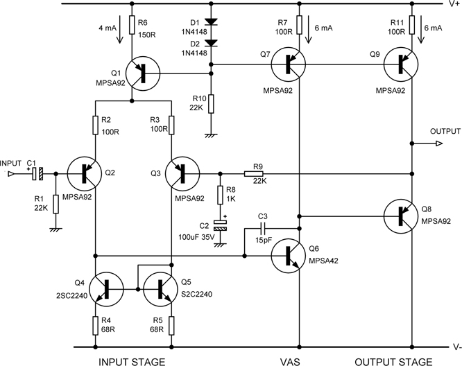
Figure 3.39 The improved discrete opamp with input pair degeneration R2, R3 and current-mirror Q4, Q5 added.
In both Figures 3.39 and 3.40, the VAS current has been increased from 1.6 mA to 6 mA. This change has very little effect on the distortion performance but much increases the positive slew rate, marking it more nearly equal to the negative slew rate. The transistors are all MPSA42/92 high-voltage low-beta types (with the exception of the current mirror) to underline the fact that high-beta devices are not required for low distortion. Do not use MPSA42 in the current mirror, as it has an unusually high minimum Vce for proper operation and so will work poorly here.
Discrete Opamp Design: The Output Stage
Figure 3.41 shows there is no need to worry about output-stage distortion with moderate loading, as it is very low with even moderate levels of NFB. If the loading is so heavy that linearity deteriorates, the options are to increase the output stage standing current or to adopt a push-pull emitter-follower output stage, as describe earlier in this chapter. The push-pull method is more efficient and will give better linearity.

Figure 3.40 The improved discrete opamp of Figure 3.39 with emitter-follower Q10 added inside the VAS local feedback loop.
For still heavier loads, a Class-AB output stage employing two complementary small-signal transistors can be used. The operation of such a stage is rather different from that of a power amplifier output stage, with crossover distortion and critical biasing being less of a problem. See Chapter 20 on headphone amplifiers for more on this.
High-Input-Impedance Bipolar Stages
Bipolar transistors are commonly thought of as low-impedance devices, but in fact they can be used to create amplifiers with extremely high input impedances. FETs are of course the obvious choice for high-input impedance amplifiers, but their lack of transconductance is a drawback. This section was inspired by an article by T. D. Towers in 1968 that is still well worth reading. [15] The circuits that follow deliberately use high-voltage low-beta transistors as higher than normal rails are one of the reasons for using discrete circuitry. ±24 V rails are used. The impedances given were measured and also checked with SPICE.
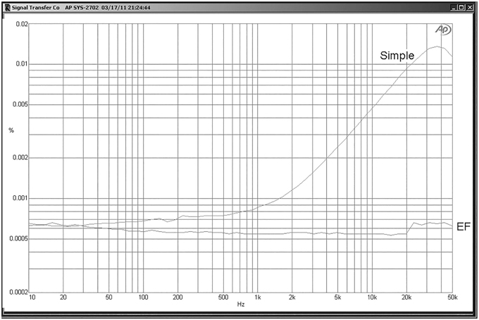
Figure 3.41 THD of the improved opamp circuit, with and without emitter-follower added to the VAS. +20 dBu output, ±20 V rails.
Figure 3.42a shows a simple emitter-follower biased by R bias, which at 100 kΩ is about as high as you would want it to be because of the voltage drop due to the base current. That limits the input impedance to 100 kΩ, of course. The First Principle of high-impedance design is to bootstrap the bias resistor as in Figure 3.42a, which raises the input impedance to 500 kΩ. You may be wondering: why not more? One reason is that Q1 is only a simple emitter-follower, and its voltage gain is distinctly less than 1, limiting the efficacy of the bootstrapping.
The Second Principle of high-impedance design with simple discrete stages is that any loading on the output reduces the input impedance because, as noted earlier:
and the bootstrap capacitor C2 is driving the load of R1 even if there is no external loading. Adding an external 10 kΩ Rload to represent the following stage reduces the input impedance to 350 kΩ.

Figure 3.42 High-impedance input stages: a) simple emitter-follower with bootstrapped biasing; 500 kΩ; b) emitter-follower with current-source and bootstrap driver stage; 6.1 MΩ; c) Darlington with current-source and bootstrap driver stage; 21 MΩ; d) Darlington with current-source and Q1 collector bootstrapped; 61 MΩ.
Having noted that both Re and Rload pull down the input impedance, we will take steps to increase their effective values. Figure 3.42b shows Re made very high by replacing the emitter resistor with a current source Q2. Rload is made high by adding simple emitter-follower Q3 to drive the bootstrap and the output. This gives a 6.1 MΩ input impedance even when driving an external 10 kΩ load output.
A further increase in input impedance can be obtained by increasing the β term in Equation 3.3 by using a Darlington configuration, where one emitter-follower feeds another, as in Figure 3.42c. Q1 must have a reasonable collector current to operate at a good β; more than the base current of Q2. An emitter resistor to the negative rail would increase the loading and defeat the object, so R4 is used, with its lower end bootstrapped from the emitter of Q2. This technique is also used in power amplifier circuitry. [16] This gives an input impedance of 21 MΩ with an external 10 kΩ load. The output is now taken from Q2 emitter once more.
To significantly further raise the input impedance, we need to take on board the Third Principle of high-impedance design: bootstrap the input transistor collector, as in Figure 3.42d. The collector resistance rc of Q1 and the base-collector capacitance cbc are both effectively in parallel with the input; the former can also be regarded as Early Effect, causing Ib to vary. Their effects are reduced by bootstrapping Q1 collector using R6 and C3. (Note that collector bootstrapping cannot be used with a single-transistor stage [17].) The emitter-follower Q4 also has its emitter-resistor replaced by current source Q5 to make its gain nearer one for more effective bootstrapping and help with driving R1 and R6. The output point has also been shifted back to the second emitter-follower. The result is an input impedance of 60 MΩ, or 50 MΩ with an external 10 kΩ load.
We have achieved this using only five transistors, so the BJT is clearly not an inherently low-impedance device. There are many more technical possibilities if you need a really astronomical input impedance; the record in 1968 appears to have been no less than 20,000 MΩ. [18]
The circuits in Figure 3.42 are not optimised for linearity. They all give substantially more distortion when fed from a high source impedance such as 1 MΩ, as the base currents drawn are not linear.
References
[1] Erdi, G. “300 V/us Monolithic Voltage Follower” IEE Journal of Solid-State Circuits, Vol. SC-14, No. 6, Dec 1979, p 1059
[2] Williams, J., ed Analog Circuit Design: Art, Science & Personalities. Butterworth-Heinemann, 1991; Chapter 21 by Barry Hilton, p 193
[3] Early, J. “Effects of Space-Charge Layer Widening in Junction Transistors” Proceedings of the IRE, Vol. 40, 1952, pp 1401–1406
[4] Tomazou, Lidgey & Haigh, eds Analogue Design: The Current-Mode Approach, p 12 et seq. IEE Circuits & Systems Series 2, 1990
[5] Feucht The Handbook of Analog Circuit Design. Academic Press, 1990, p 484 et seq
[6] Self, Douglas Audio Power Amplifier Design Handbook 5th edition. Newnes, p 78
[7] Nelson-Jones, L. “Wideband Oscilloscope Probe” Wireless World, Aug 1968, p 276
[8] White, Eric “Improvements in or Relating to Thermionic Valve Amplifier Circuit Arrangements” British Patent No 564,250 (1940)
[9] Feucht, D. L. The Handbook of Analog Circuit Design. Academic Press, 1990, p 310 et seq
[10] de Lange “Flat Wideband Buffers” Electronics World, Oct 2003, p 19
[11] Staric & Margan Wideband Amplifiers. Springer, 2006 Chapter 5, p 5.117 (HB) (Schlotzaur)
[12] Self, Douglas “A High-Performance Preamplifier Design” Wireless World, Feb 1979
[13] Self, Douglas “An Advanced Preamplifier Design” Wireless World, Nov 1976
[14] Self, Douglas Audio Power Amplifier Design 6th edition, Newnes, 2013
[15] Towers, T. D. “High Input-Impedance Amplifier Circuits” Wireless World, Jul 1968, p 197
[16] Self, Douglas Audio Power Amplifier Design 6th edition. Newnes, 2013, p 190
[17] Johnson, P. A. Comment on “High Input-Impedance Amplifier Circuits” Letters, Wireless World, Sept 1968, p 303
[18] Horn, G. W. “Feedback Reduces Bio-Probe’s Input Capacitance” Electronics, 18 Mar 1968, pp 97–98