CHAPTER 10
Moving-Coil Head Amplifiers
Moving-coil cartridges are generally accepted to have a better tracking performance than moving-magnet cartridges because the moving element is a set of lightweight coils rather than a magnet, which is inevitably made of a relatively dense alloy. Because the coils must be light, they consist of relatively few turns, and the output voltage is very low, typically in the range 100 to 550 μVrms at a velocity of 5 cm/sec, compared with 5 mVrms from the average moving-magnet cartridge. Fortunately, this low output comes from a very low impedance, which, by various technical means, allows an acceptable signal-to-noise performance to be obtained.
Moving-Coil Cartridge Characteristics
There is much greater variation in impedance and output across the available range of moving-coil cartridges than for moving-magnet cartridges. The range quoted above is already much wider, but including the extremes currently on the market (2019), the output range is from 40 to 2500 μV, a remarkably wide span of 62 times or 36 dB. This is illustrated in Figure 10.1, which shows the results of a survey of 85 different MC cartridges. (Note that the ranges for the columns are wider at the right side of the diagram.) When I first became involved in designing MC amplifiers in 1986, I compiled a similar chart [1], and it is interesting to note that the same features occurred –there are two separate clusters around 100–300 μV and 500–700 μV, and the lowest output is still 40 μV from an Audio Note cartridge (the loLtd model). The highest output of 2.5 mV comes from the Benz Micro H2, and this is only 6 dB below an MM cartridge.
Assuming that a conventional MM input stage is being used to raise 5 mV to nominal internal level and perform the RIAA equalisation, the Audio Note cartridge requires a gain of 125 times or +42 dB to reach 5mV. The cartridge cluster around 200 μV output needs 25 times or +28 dB, while the 500 μV cluster requires 10 times or +20 dB. If an amplifier is to cover the whole range of MC cartridges available, some form of gain switching is highly desirable.
Cartridge impedances also vary markedly, over a range from 1 Ω (Audio Note loLtd) to 160 Ω (Denon DL-110 and DL160), with impedance increasing with output level, as you would expect –there are more turns of wire in the coils. The inductance of MC cartridges is very low, and their source impedance is normally treated as purely resistive. The recommended load impedances are also resistive (unlike the R-C combinations often used with MM cartridges) and are usually quoted as a minimum load resistance. Once more the variation is wide, from 3 Ω (Audio Note loLtd again) to 47 kΩ (Denon DL-110 and DL160 again), but a 100 Ω input load will be high enough for most of the cartridges surveyed, and 500 Ω will work for almost all of them. The Audio Note loLtd cartridge is unusual in another way –its magnetic field is produced not by permanent magnets but a DC-powered electromagnet, which presumably requires a very pure supply indeed. The manufacturers whose cartridges were included in the survey are listed in Table 10.1.
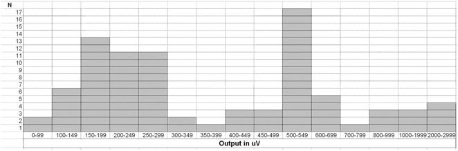
Figure 10.1 The output levels for 85 moving-coil cartridges at 5 cm/sec (2009).
| Audio Note | Immutable Music |
|---|---|
| Benz Micro | Koetsu |
| Cardas | Lyra |
| Clear Audio | Miyabi |
| Denon | Ortofon |
| Dynavector | Shelter |
| Goldring | Sumiko |
| Grado | van den Hul |
The Limits on MC Noise Performance
Because MC cartridges can be modelled for noise purposes simply as their coil resistance, it is straightforward to calculate the best signal/noise ratio possible. Even if we assume a noiseless amplifier, the Johnson noise from the coil resistance sets an inescapable limit; comparing this with the cartridge nominal output gives the maximum signal/noise ratio. This was done for all the cartridges used to compile Figure 10.1, using the manufacturer’s specs, and the answers varied from 63.9 to 90.8 dB, which is a pretty big spread. (This does not include RIAA equalisation.)
In practice, things will be worse. Even if we carry on assuming a noiseless amplifier, there is resistance in the tone-arm wiring, which has to be very thin for flexibility, and a bit more in the cable connecting turntable to preamp. Calculating the same figures for MM cartridges is a good deal more complicated because of the significant cartridge inductance; see Chapter 9.
Amplification Strategies
There are two ways to achieve the high gains required for these low-output cartridges. In the most common method, a standard MM input stage, with RIAA equalisation, can be switched to either accept an MC input directly, or the output of a specialised MC input stage which gives the extra gain needed; this may be either a step-up transformer or an amplifier configured to give low noise with very low source resistances. The large amount of gain required is split between two stages, which makes it easier to achieve. Alternatively, a single stage can be used with switched gain; but this is not too hot an idea:
- Switchable gain makes accurate RIAA equalisation harder, but see Chapter 9 for gain-switching options.
- For good noise performance, a BJT input device operating current needs to be low for MM use (where it sees a high impedance) and high for MC use (where it sees a very low impedance). Making this operating current switchable would be a complicated business. Using a JFET instead solves the problem. See Chapter 9.
- Achieving the very high gain required for MC operation together with low distortion and adequate bandwidth will be a challenge. It is unlikely to be possible with a single opamp, and so there is little likelihood of any saving on parts.
Moving-Coil Transformers
If you have a very low output voltage and very low impedance, an obvious way to deal with this is by using a step-up transformer to raise the voltage to the level at which it can be appropriately applied to a moving-magnet amplifier stage, such as those discussed in Chapter 9. Such a transformer has most of the usual disadvantages such as frequency response problems and cost, though for hi-fi use, the weight is not a difficulty, and non-linearity should not be an issue because of the very low signal levels.
In this application, the cost is increased by the need for very high immunity to hum fields. While it is relatively straightforward to make transformers that have high immunity to external magnetic fields, particularly if they are toroidal in construction, it is not cheap, because the mu-metal cans that are required for the sort of immunity necessary are difficult to manufacture. The root of the problem is that the signal being handled is so very small. The transformer is usually working in a modern house, which can have surprisingly large hum fields and generally presents a hostile environment for very-low-signal transformers, so very good immunity indeed is required; some manufacturers use two nested screening cans, separately grounded, to achieve this, as shown in Figure 10.2. An inter-winding electrostatic screen is usually fitted. A stereo MC input naturally requires two of these costly transformers.
MC transformers are designed with low primary winding resistances, typically 2 or 3 Ω, to minimise the Johnson noise contribution from the transformer. Some transformers have windings made of silver rather than copper wire, but the conductivity of silver is only 5% higher than that of copper, and the increase in cost is startling. At the time of writing, one brand of silver-wound transformer costs more than £1200 – each, not for a pair.
Because of the great variation in cartridge output levels and impedances some manufacturers (e.g. Jensen) offer transformers with two or three primary windings, which can be connected in series, parallel, or series-parallel to accommodate a wide variety of cartridges.
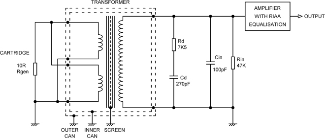
Figure 10.2 A typical MC step-up transformer circuit with twin primaries wired in parallel, dual screening cans, and Zobel network Rd, Cd across the secondary. Rin, Cin are the usual MM input loading components.
A transformer secondary must be correctly loaded to give the flattest possible frequency response, and this usually means that a Zobel R-C network must be connected across it, as explained in Chapter 18 on line inputs. This is Rd and Cd in Figure 10.2, where they have typical values. The values required depend not only on the transformer design but also somewhat on the cartridge impedance, and some manufacturers such as Jensen are praiseworthily thorough in giving secondary loading recommendations for a wide range of cartridge impedances.
The very wide variation in cartridge outputs means that the step-up ratio of the transformer must be matched to the cartridge to get an output around 5 mV that is suitable for an MM input amplifier. For example, Jensen offers basic step-up ratios from 1:8 to 1:37. The maximum ratio is limited not only by transformer design issues but by the fact that the loading on the secondary is, as with all transformers, transferred to the primary divided by the square of the turns ratio. A 1:37 transformer connected to the 47 kΩ input impedance of an MM stage will have an impedance looking into the primary of only 34 Ω; such a transformer would, however, only be used with a very low-impedance low-output cartridge, which would be quite happy with such a loading. It is of course possible to arrange the input switching so the 47 kΩ input load is on the MM socket side of the MC/MM switch; the MM amplifier can then have a substantially higher input impedance.
Moving-Coil Input Amplifiers
The high cost of transformers means that there is a strong incentive to come up with an electronic solution to the amplification problem. The only thing that makes it possible to achieve a reasonable signal-to-noise ratio is that the very small signal comes from a very low source impedance.
MC head amplifiers come in many forms, but almost all in use today can be classified into one of the topologies shown in Figure 10.3, all of which use series feedback. The configuration in Figure 10.3a is a complementary-feedback pair using a single input transistor chosen to have a low base series resistance Rb. The feedback network must also have a low impedance to prevent its Johnson noise from dominating the overall noise output, and this puts a heavy load on the second transistor. Typically a gain of 47 times will be implemented with an upper feedback resistor of 100 Ω and a lower resistor of 2 Ω, a total load on the amplifier output of 102 Ω. The combination of limited open-loop gain and the heavy load of the feedback network means that both linearity and maximum output level tend to be uninspiring, and the distortion performance is only acceptable because the signals are so small. An amplifier of this type is analysed in [2].
Figure 10.3b shows a classic configuration in which multiple transistors are operated in parallel so that their gains add but their uncorrelated noise partly cancels. Two transistors gives a 3 dB improvement, 4 transistors 6 dB, and so on. The gain block A is traditionally one or two discrete devices, which again have difficulty in driving the low-impedance feedback network. Attention is usually paid to ensuring proper current-sharing between the input devices. This can be done by adding low-value emitter resistors to swamp Vbe variations; they are effectively in series with the input path and therefore degrade the noise performance unless each resistor is individually decoupled with a large electrolytic. Alternatively, each transistor can be given its own DC feedback loop to set up its collector current. For examples of this kind of circuitry, see [3].
Figure 10.3c shows the series-pair configuration. This simple arrangement uses two complementary input transistors to achieve a 3 dB noise improvement without current-sharing problems, as essentially the same collector current goes through each device. The collector signal currents are summed in Rc, which must be reasonably low in value to absorb collector-current imbalances. There is no feedback, so linearity is poor. The biasing arrangements are not shown.
Figure 10.3d is an enhancement of Figure 10.3a, with the input transistor inverted in polarity and the spadework of providing open-loop gain and output drive capability entrusted to an opamp. The much increased feedback gives excellent linearity, and less than 0.002% THD at full output may be confidently expected. However, problems remain. Rf2 must be very low in value, as it is effectively in series with the input and will degrade the noise performance accordingly. If Rf2 is 10 Ω (which is on the high side), Cf must be very large, for example 1000 μF to limit the LF roll-off to -1 dB at 30 Hz. Adopting a quieter 3.3 Ω for the Rf2 position gives significantly lower noise but demands 4700 μF to give −3 dB at 10 Hz; this is not elegant and leads to doubts as to whether the ESR of the capacitor will cause trouble. Cf is essential to reduce the gain to unity at DC because there is +0.6 V on the input device emitter, and we don’t want to amplify that by 50 times.
The +0.6 V offset can be eliminated by the use of a differential pair, as in Figure 10.3e. This cancels out the Vbe of the input transistor TR1, at the cost of some degradation in noise performance. The pious hope is that the DC offset is so much smaller that if Cf is omitted and the offset is amplified by the full AC gain, the output voltage swing will not be seriously reduced. The noise degradation incurred by using a differential pair was measured at about 2.8 dB. Another objection to this circuit is that the offset at the output is still non-negligible, about 1V, mostly due to the base bias current flowing through R10. A DC-blocking capacitor on the output is essential.
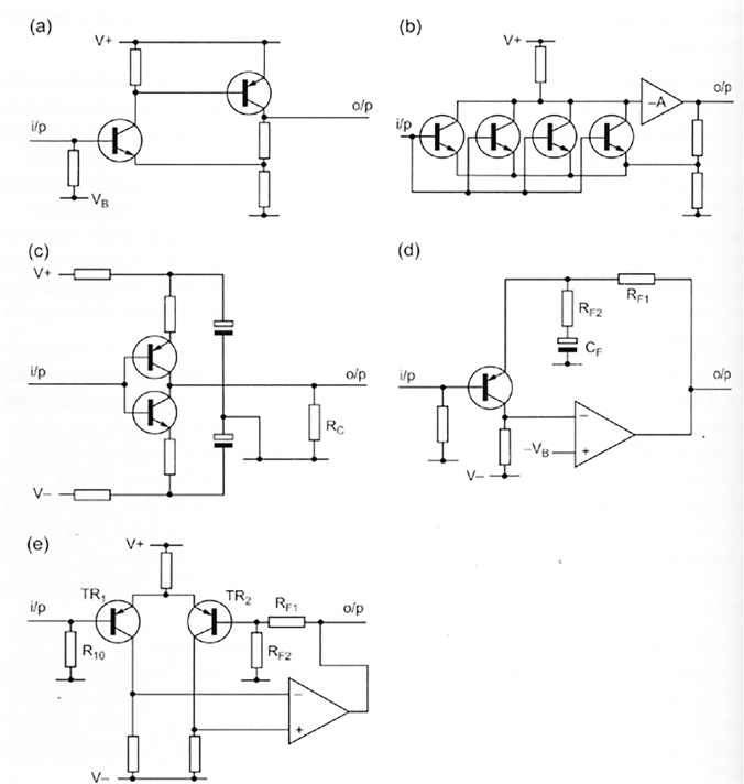
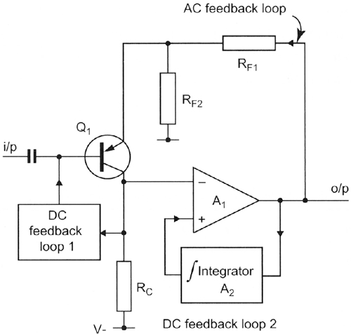
Figure 10.4 Block diagram of the MC preamplifier showing the two DC feedback loops.
An Effective MC Amplifier Configuration
Finding none of these configurations satisfactory, I evolved the configuration shown as a block diagram in Figure 10.4. There is no Cf in the feedback loop and, indeed, no overall DC feedback at all. The input transistor and the opamp each have their own DC feedback systems. The transistor relies on simple shunt negative feedback via DC loop 1; the opamp has its output held precisely to a DC level of 0 V by the integrator A2, which acts as DC loop 2. This senses the mean output level and sets up a voltage on the non-inverting input of A1 that is very close to that at Q1 collector, such that the output stays firmly at zero. The time-constant is made large enough to ensure that an ample amount of open-loop gain exists at the lowest audio frequencies. Too short a time-constant will give a rapid rise in distortion as frequency falls. Any changes in the direct voltage on Q1 collector are completely uncoupled from the output, but AC feedback passes through Rf1 as usual and ensures that the overall linearity is near-perfect, as is often the case with transistor opamp hybrid circuits. Due to the high open-loop gain of A, the AC signal on Q1 collector is very small and so shunt AC feedback through DC loop 1 does not significantly reduce the input impedance of the overall amplifier, which is about 8 kΩ.
As we have seen, MC cartridges vary greatly in their output, and different amplifier gain settings are highly desirable. Usually it would be simple enough to alter Rf1 or Rf2, but here it is not quite so simple. The resistance Rf2 is not amenable to alteration, as it is kept to the low value of 3.3 Ω by noise considerations, while Rf1 must be kept up to a reasonable value so that it can be driven to a full voltage swing by an opamp output. This means a minimum of 500 Ω for the 5534/2. It is intriguing that amplifiers whose output is measured in millivolts are required to handle so much current.
These two values fix a minimum closed-loop gain of about 44 dB, which is much too high for all but the most insensitive cartridges. My solution was to use a ladder output attenuator to reduce the overall gain; this would be anathema in a conventional signal path because of the loss of headroom involved, but since even an output of 300 mVrms would be enough to overload virtually all MM amplifiers, we can afford to be prodigal with it. If the gain of the head amplifier is set to be a convenient 200 times (+46 dB), then adding output attenuation to reduce the overall gain to a more useful +20 dB still allows a maximum output of 480 mVrms. Lesser degrees of attenuation to give intermediate gains allow greater outputs, and these are summarised in Table 10.2. For testing, an Ortofon MC10 was used with +26 dB of gain, giving similar output levels to MM cartridges. This highly successful cartridge was in production for 30 years and has only recently been superseded; its impedance is 3.3 Ω.
| Gain | Gain (dB) | Max output (rms) |
|---|---|---|
| 10 x | +20 dB | 480 mV |
| 20 x | +26 dB | 960 mV |
| 50 x | +34 dB | 2.4 V |
| 100 x | +40 dB | 4.6 V |
| 200 x | +46 dB | 10 V |
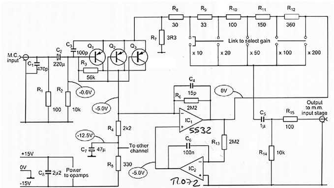
A final constraint on the attenuator is the need for low output impedances so the succeeding MM input stage can give a good noise performance. The MM input should have been optimised to give its best noise figure with relatively high source impedances, but a low source impedance will still reduce its actual noise output. This means that an output attenuator will need low resistor values, imposing yet more loading on the unfortunate opamp. This problem was solved by making the attenuator ladder an integral part of the AC feedback loop, as shown in Figure 10.5. This is practicable because it is known that the input impedance of the following MM stage will be too high at 47 kΩ to cause significant gain variations.
The Complete Circuit
This is shown in Figure 10.5 and closely follows Figure 10.4, though you will note that the input devices have suddenly multiplied themselves by three. Capacitor C1 is soldered on the back of the MC input phono sockets and is intended for EMC immunity rather than cartridge response modification. If the need for more capacitive or resistive loading is felt, then extra components may be freely connected in parallel with R1. If R1 is raised in value, then load resistances of 5 kΩ or more are possible, as the impedance looking into C2 is about 8 kΩ. Capacitor C2 is large to give the input devices the full benefit of the low source impedance, and its value should not be altered. Resistors R2, R3 make up DC loop 1, setting the operating conditions of Q1, Q2, Q3, while R4 is the collector load, decoupled from the supply rail by C7 and R5, which are shared between two stereo channels.
Opamp IC1 is a half of a 5532, providing most of the AC open-loop gain, and is stabilised at HF by C4. R6 has no real effect on normal operation, but is included to give IC1 a modicum of DC negative feedback and hence tidy behaviour at power-up, which would otherwise be slow due to the charging time of C2. IC2, half of a TL072, is the integrator that forms DC loop 2, its time-constant carefully chosen to give ample open-loop gain from IC1 at low frequencies while avoiding peaking in the LF response that could occur due to the second time-constant of C2.
The ladder resistors R8–R12 make up the combined feedback network and output attenuator, the gain being selected by a push-on link in the prototype. A rotary switch could be used instead, but this should not be operated with the system volume up, as this will cause loud clicks due to the emitter current (about 4 mA) of Q1–Q3 flowing through R7, which causes voltage drops down the divider chain. Note that the current through R7 flows down the ground connection back to the PSU. Output resistor R15 ensures stability when driving screened cables, and C5 is included to eliminate any trace of DC offset from the output.
The power supply rails do not need to be specially quiet, and a normal opamp supply is quite adequate.
Performance
The input transistor originally chosen was the 2N4403, a type that was acknowledged as superior for this kind of application for some years due to its low Rb of about 40 Ω. A single device used in the circuit of Figure 10.5 gives an EIN of −138 dB with a 4 mA collector current and a 3.3 Ω source resistance. The Johnson noise from 3.3 Ω is -147.4 dBu, so we have a noise figure of 9.4 dB. It was then consistently found that putting devices in parallel without any current-sharing precautions whatever always resulted in a significant improvement in noise performance. On average, adding a second transistor reduced noise by 1.2 dB, and adding a third reduced it by another 0.5 dB, giving an EIN of -139.7 dBu and an NF of 7.7 dB. Beyond this, further multiplication was judged unprofitable, so a triple-device input was settled on. The current sharing under these conditions was checked by measuring the voltage across 100 Ω resistors temporarily inserted in the collector paths. With 3.4 mA as the total current for the array, it was found after much device swapping that the worst case of imbalance was 0.97 mA in one transistor and 1.26 mA in another. The transistors were not all from the same batch. It appears that, for this device at least, matching is good enough to make simple paralleling practical.
A superior device for low source impedances was the purpose-designed 2SB737, with a stunningly low Rb of 2 Ω. Three of them improved the EIN to -141.0 dBu and the NF to 6.4 dB, albeit at significant cost. Sadly it is now obsolete (why, for heaven’s sake?) but can still be obtained from specialised suppliers such as the Signal Transfer Company. [4]
You will have spotted that R7, at 3.3 Ω, generates as much noise as the source impedance; this only degrades the noise figure by 1.4 dB rather than 3 dB, as most of the noise comes from the transistors.
It would be instructive to compare this design with other MC preamplifiers, but it is not at all easy, as their noise performance is specified in so many different ways it is virtually impossible to reduce them all to a similar form, particularly without knowing the spectral distribution of the noise. (This chapter has dealt until now with unweighted noise referred to the input, over a 400 Hz–20 kHz bandwidth, and with RIAA equalisation not taken into account.) Nonetheless, I suggest that this design is quieter than most, being within almost 6 dB of the theoretical minimum, and so with limited scope for further improvement. Burkhard Vogel has written an excellent article on the calculation and comparison of MC signal-to-noise ratios [5], and this has been much expanded and incorporated in his remarkable book The Sound of Silence and goes into more detail than there is space for here. [6] It is highly recommended.
| Input overload level | 48 mVrms |
| Equivalent input noise | −141.0 dBu, unweighted, without RIAA equalisation (3.3 Ω source res) |
| Noise figure | 6.4 dB (3.3 Ω source res) |
| THD | Less than 0.002% at 7 Vrms out (maximum gain) at 1 kHz Less than 0.004% 40 Hz–20 kHz |
| Frequency response | +0, −2 dB, 20 Hz–20 kHz |
| Crosstalk | Less than −90 dB, 1 kHz–20 kHz (layout dependent) |
| Power consumption | 20 mA at ±15 V, for two channels |
The performance is summarised in Table 10.3. Careful grounding is needed if the noise and crosstalk performance quoted is to be obtained.
When connected to a RIAA-equalised MM stage as described in Chapter 9, the noise output from the MM stage is -93.9 dBu at 10 times MC gain and -85.8 dBu at 50 times. In the 10 times case, the MC noise is actually 1.7 dB lower than for MM mode.
References
[1] Self, Douglas “Design of Moving-Coil Head Amplifiers” Electronics & Wireless World, Dec 1987, p 1206
[2] Nordholt & Van Vierzen “Ultra Low Noise Preamp for Moving-Coil Phono Cartridges” JAES, Apr 1980, pp 219–223
[3] Barleycorn, J. (a.k.a. S. Curtis) HiFi for pleasure, Aug 1978, pp 105–106
[4] Signal Transfer Company www.signaltransfer.freeuk.com/
[5] Vogel, Burkhard “The Sound of Silence” (Calculating MC preamp noise) Article in Electronics World, Oct 2006, p 28
[6] Vogel, Burkhard The Sound of Silence 2nd edition. Springer-Verlag, 2011 Chapters 15, 16.