CHAPTER 22
Mixer Sub-Systems
This chapter deals with the specialised circuit blocks that make up mixing consoles. Some functions, such as microphone amplification, line input and output, and equalisation have already been explored in previous chapters. The other useful blocks are presented in the order that a signal encounters them as it goes through the console, but many of them are applicable to all the various kinds of module – input channels, groups, and master sections. For example, fader post-amplifiers and insert points will be found in all three types of module.
Mixer Bus Systems
In all but the smallest mixers, there is a need to connect together all the modules so they have access to the mixing buses, power supply rails, and logic and control lines.
There are three basic ways of connecting together the modules. The smallest mixers are usually constructed on a single large PCB lying parallel to a one-piece front panel, and here “modules” means repeated circuitry rather than physical modules. The all-embracing PCB minimises the money spent on connectors and the time plugging them in during assembly, but there are obvious limitations to the size of mixer you can build in this way. A definite problem is the need to run summing buses laterally, as this results in them winding their way between controls and circuit blocks, threatening a mediocre crosstalk performance. The use of double-sided PCBs helps greatly with this, but very often there are still awkward points such as the need for the feed to and from the faders to cross over the mix bus area. This can easily wreck the crosstalk performance; one solution is to use what I call a “three-layer board” (See Chapter 2). The mix buses are on the bottom of the PCB, the top layer above it carries a section of ground plane, and the fader connections are made by wire links above that. Given a tough solder-resist, no further insulation of the links is necessary; if you have doubts, then laying a rectangle of component-ident screen print under the links will give another layer of insulation without adding labour cost.
Medium-sized mixers are commonly made with separate modules, connected together with ribbon cable bearing insulation-displacement connectors. The advent of IDC ribbon cables (a long time ago, now) had a major effect on the affordability of mixing consoles. These cables naturally join Pin 1 to Pin 1 on every module, and so on, leading to a certain inflexibility in design.
Large mixers use a motherboard system, where each module plugs into a PCB at the bottom of the frame, which is typically divided into “bins” holding 8 or 12 modules. This provides (at considerably increased expense) total flexibility in the running of buses and the interconnection of modules.
To me, it is a “mixing bus” or a “summing bus”. I realise that some of the world spells it “buss”, and I am probably wasting my time pointing out that the latter is wrong, but I am still going to do it. The term dates from the dawn of electrical distribution, when circuits where connected together by copper bars called “omnibus bars”. This inevitably got shortened to “bus-bars”, and in mixing consoles it was further abbreviated to “bus”, which somehow turned into “buss”. The Oxford English Dictionary says buss means “to kiss” (archaic), which seems somehow not quite appropriate. Unless of course you’re recording Kiss. I have grave doubts if my protest here will make any difference to common usage, but sometimes you’ve just got to make a stand.
Input Arrangements
Most mixer channels have both microphone and line inputs. On the lower-cost consoles, these are usually switched to a single amplifier with a wide gain range, the line input being attenuated to a suitable level first. This approach is covered in Chapter 17 on microphone amplifiers. High-end consoles have separate line input amplifiers, removing some compromises on CMRR and noise performance. Dedicated line input amplifiers are dealt with in Chapter 18.
Equalisation
Mixer input channels have more or less sophisticated tone controls to modify the frequency response, either to correct imperfections or to produce specific effects. This subject is fully dealt with in Chapter 15.
Insert Points
The addition of effects for general use, such as reverberation, is normally handled by an effects send system. However, if a specific effect (say, flanging) is going to be used on one channel only, then it is far more efficient and convenient to connect the external effects unit in series with the signal path of the channel itself. This is done by means of an insert point (usually just called an “insert”), which is a jack with normalling contacts arranged so that the signal flows to it and back to the channel again when nothing is plugged in. When a jack is inserted, the normalling connection is broken and the signal flows through the external unit. Inserts are also often fitted to groups.
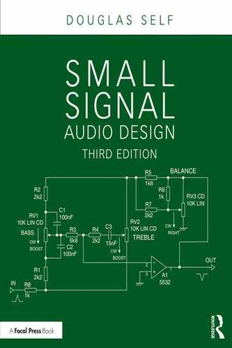
Inserts come in two versions, illustrated in Figure 22.1. The single-jack version is economical in panel space but is restricted to unbalanced operation. The two-jack version is superior because it allows the use of balanced send and returns, and in addition, the OUT jack socket can be used as a direct output because inserting a jack in it does not break the signal path; only inserting a jack into the IN jack socket does that.

Figure 22.1 The single-jack insert a) and the two-jack insert b).
When the mixer has a patchbay, the insert sends (and indeed, other console outputs) are likely to find their way there through a quite considerable length of ribbon cable, which has significant capacitance between its conductors. It is easy to get into a situation where the crosstalk performance of the console is limited by capacitive crosstalk between outputs, despite their low impedance. Output amplifiers commonly have a series resistor to isolate the amplifier from the capacitance of the cabling and prevent HF instability, and the minimum safe value of this resistor defines the output impedance, which is usually in the region of 47 to 100 Ω. Things get worse when the layers of ribbon cable are laid together in a “lasagne” format; this is very often necessary because of the sheer number of signals going to and from the patchbay. In some cases, layers of grounded screening foil are interleaved with the cables, but this is rather expensive and awkward to do and does not greatly reduce crosstalk between conductors in the same piece of ribbon. The only way to do this is to reduce the output impedance.
In a particular mixer design project, the crosstalk between the insert sends from the channels, with an output impedance of 75 Ω, was found to be -96 dB at 10 kHz. This may not sound like a lot, but I didn’t get where I am today by designing consoles with measurable crosstalk, so something had to be done. An effective way to obtain a near-zero output impedance is shown in Figure 22.2. Here the main negative feedback for the opamp goes through R1 from the outside end of isolating resistor R2 and so reduces the output impedance, while the stabilising HF feedback is taken through C1 from the inside end, where it is not subject to phase shift because of load capacitance. With this insert send stage, the output impedance was reduced from 75Ω to less than 1Ω, and the crosstalk disappeared below the noise floor. Very similar circuitry can be used with stages that have gain. Arrangements like this must always be carefully checked to make sure that HF stability with a capacitive load really is maintained; this circuit is stable when driving a 22 nF load, which represents 220 metres of 100pF/metre cable; see Chapter 19 for more on this.
This arrangement is sometimes called a “zero-impedance” output; the impedance is certainly much lower than usual, but it is not of course actually zero.
Figure 22.2 A typical non-inverting insert-send amplifier with “zero-impedance” output.
In a group module, an inverting insert send amplifier is often used to correct the phase inversion introduced by the summing amplifier. A zero-impedance version of this is illustrated in the section on summing amplifiers.
How to Move a Circuit Block
In the more sophisticated and versatile mixers, it is often possible to rearrange the order of blocks in the signal path. A typical example is the facility to move an insert point from before to after the EQ section, depending on what sort of external processing is being plugged into the insert. Dynamics sections are also often movable to pre or post the EQ.
Figure 22.3 shows two ways to move a circuit block from one position to another in the signal path. The version at Figure 22.3a uses all the sections of a four-changeover switch to do the job. Normally the insert is before the EQ section, but when the switch, which would probably be labelled “insert post” or whatever abbreviation of that can be fitted in, is pressed the signal passes along path A and reaches the EQ first; it then goes back through path B, through the insert, and then to the output along path C. However, the existence of two unused switch contacts gives us a broad hint that there may be a more efficient way to do it.
There certainly is; Figure 22.3b shows how to do it with only three changeovers. When the switch is pressed, the signal passes along path A and reaches the EQ first, goes back through path B to the insert, and then out via path C. You might think that this economy is quite pointless, because either way you will need to use a physical four-changeover switch, but in fact, the spare switch section in Figure 22.3b comes in very handy indeed to operate a switch-status indicator LED. Alternatively the spare switch section can be connected in parallel with one of the other sections in the hope of improving reliability, but…
Paralleling switch sections sounds as though it would massively increase reliability, but it is actually not as useful as you might think. The classic switch problem is contamination of silver-plated contacts; the silver is converted to non-conductive silver sulphide by the action of hydrogen sulphide in the atmosphere. This can come from industrial pollution, but another source is diesel engine exhaust, so virtually nowhere can be assumed to be free of it. If one set of contacts in a switch is affected, then the other set right next to it is certain to be affected also, and paralleling the contacts is actually of little or no use. Sad but true.

Faders
So far as circuit design is concerned, a slide fader can normally be regarded as simply a logarithmic potentiometer, though in fact its internal construction may be quite complicated. The technology of faders is dealt with in Chapter 13 on volume controls and is not repeated here.
However, here is one anecdote that may yet have its uses. Connections to and from the fader are normally done by two individually screened cables. The send wire must be stopped from radiating and the return wire stopped from both radiating and picking stuff up. The return wire will be quite susceptible to pick-up in some fader positions, and it should always be screened. However, I recall an application in which there was no sensitive circuitry nearby, and there was no need to screen the send wire. This was therefore an unscreened wire (coloured red to indicate send) that spiralled around the screened return wire. The spiralling was nothing to do with inductance – it just physically located the send wire. This saved quite a bit of time on making up fader connection harnesses.
Improving Fader Offness
This information is placed here rather than in Chapter 13, as it deals with circuitry around the fader rather than the fader itself.
For quite a long time in the mixer business, lower-cost-bracket consoles used slide potentiometers rather than the precision faders made by people like Penny and Giles. These low-cost faders had a poor feel compared with the top-end faders, but their worst characteristic was poor offness due the resistance where the connection was made to the end of the carbon track. This was usually of the order of -90 dB rather than the -120 dB or more you would expect from a top-end part. Low-cost faders did not use “infinity-off” construction (see Chapter 13).
This meant that it was the fader that defined the general signal cleanliness of a mixing console; as described later in this chapter, getting good routing offness had been sorted out several years earlier. While at Soundcraft, I decided to do something about this. The key to the problem was that the offness of the faders used, while not very good, was quite consistent. This suggested that taking the signal from the top of the fader and feeding a tiny amount of it to the post-fade amplifier in anti-phase would give a worthwhile amount of cancellation, and so it proved. Figure 22.4a shows two ways to implement the idea. The post-fade amplifier has a very convenient “inverting input” in that a high-value resistor can be connected to the negative-feedback arm as in Figure 22.4a. An appropriate choice for R5 improved the offness by a dependable 15 dB and often more across the audioband; there are no variations with frequency. Note that R5 was a fixed value and not adjusted-on-test, which would have been uneconomic; however, periodic offness checks were undertaken to make sure the fader characteristics had not changed.

Figure 22.4 Improving the offness of a low-cost fader by cancellation: a) using a single feedforward resistor; b) using two resistors to give more control over the amount of anti-phase feedforward.
A more flexible method is shown in 22.4b; the amount of anti-phase feedforward is now determined by two resistors, R5 and R4, which gives much more scope, as both values can be juggled to give on average good cancellation. I must emphasise that while this method can be highly effective, it does depend on consistency in the fader offness.
The first method was used in the Soundcraft Sapphyre input/output module, and the second was used on the Soundcraft Delta-SR mono input module and stereo input module (1992).
Post-Fade Amplifiers
The post-fade amplifier (sometimes called just the post amp) comes just after the fader, as its name implies. Its primary function is to allow the fader section to give gain. A +10 dB post amplifier, which is the most common amount of gain, allows the fader to be calibrated up to +10 dB. The 0 dB setting is then some way down the scale, and it is much easier to adjust the channel level up and down with respect to the rest of the mix. Without this feature, if a channel was fully faded up at 0 dB, to increase its relative level, it would be necessary to pull all the other faders down. When you consider that a large mixer may have 64 channel faders, you can see that this would be something of a nuisance.
The second function of the post amp is to buffer the fader from the heavy loading of panpot, mix resistors, and aux sends. The fader control law is carefully chosen for optimal controllability, and that law would be seriously distorted if all that loading came directly on the fader wiper.
It is important that the post-fade amp has good noise performance, because its noise contribution is not much reduced when the fader is pulled down, and it must also have a good load-driving capability at low distortion. For these two reasons, the 5534/2 opamp found a home in post amps quite early in its history, when its high cost ruled it out for most other circuit functions, which were still handled by TL072s. The other place that 5534/2s appeared early was in summing amplifiers, which often work at a high noise gain.
However, in budget designs TL072s or equivalent FET-input opamps are still used because they are not only cheaper themselves but allow several other parts to be omitted. In Figure 22.5a, the opamp input can be directly connected to the fader wiper because the input bias current is negligible and does not cause significant noise when the wiper is moved along the track. Note that the gain-determining resistors R2, R3 have to be quite high to minimise the loading on the opamp output. C3 improves stability.
In a more sophisticated design as in Figure 22.5b, the use of a 5534 with its significant bias current means that DC blocking capacitor C1 is required to prevent unpleasant sounds when the fader is adjusted; in turn, this means that R1 is required to bias the opamp. Another consequence flows from this; R1 has to have a relatively high value so it does not load the fader and distort its control law, and so the 5534 input bias current causes a relatively large offset voltage at the opamp input. The 5534 max bias current is 800 nA, which means a possible drop across R1 of -37.6 mV. The 5534 has NPN input devices, so the bias current flows into the input pins, and so this voltage is negative, and that is why C1 is the way round it is. This input offset appears multiplied by three at the post amp output, giving -113 mV. This is not enough to significantly affect the available output swing, but it does mean that C2 must be introduced to keep DC out of the panpot and post-fade sends. Since the loading is quite heavy, C2 must be large to prevent it creating distortion (see Chapter 2). Note also the polarity of C2. We now have not only a more expensive opamp with a higher power consumption but three extra components. Their number is multiplied by N, the number of channels, so you can see that the use of the 5534 as a post amp was actually a more serious cost decision than it might appear.

Figure 22.5 Three versions of a post-fade amplifier. That at a) is the cheap and cheerful version, while b) is the more up-market version, with pre and post sends and the panpot section of a mixer channel shown, and c) protects the opamp against capacitive loading while still giving a “zero-impedance” output.
You will note that in Figure 22.5b, the resistors R2, R3 in the feedback network have been reduced in value by a factor of about two to improve the noise performance. However, they are still not particularly low in value, and it is true that the noise performance could be improved if they were reduced to, say, 680 Ω and 330 Ω, which in itself would be well within the drive capability of a 5532. However, in simpler desks, this opamp has to drive not only its own feedback network but also the panpot, routing matrix, and the post-fade sends, and most of its drive capability has to be reserved for this duty.
Figure 22.5c shows a post amp utilising the “zero-impedance” approach described for insert send amplifiers. In some layouts, the panpot, routing, and post-fade sends are physically spread out so that the stray capacitance seen by the post amp output is enough to imperil its stability. An output isolating resistor R4 cures the problem but, if simply stuck in the output line, causes the level after it to vary as changing panpot and send settings alter the load on it. The feedback resistor R2 is therefore fed from after R4, preserving the “zero-impedance” output, but C3 is fed from before it, maintaining the HF stability.
Fader post amps almost invariably have a fixed gain; if they did not, the carefully designed fader law would no longer be obtained. However, there are places where making the gain effectively variable by the use of positive feedback allows the post amp to have a low gain when its associated control is at a low setting; this minimises the noise contribution of the post amp. There is more on this technique in the section on aux masters.
Direct Outputs
In more complex consoles, a direct out is available from each channel. This is a post-fade signal, which can be fed directly to a recording device without sending it through the routing and summing systems. This gives a minimum signal path which will exhibit less noise and possibly less distortion. In all except the most elaborate consoles, the direct out tends to be unbalanced, to save hardware, and reliance is placed on the recording device having balanced inputs.
Many Soundcraft mixers used ground-cancelling direct outputs, giving most of the benefits of a balanced link when plugged into an unbalanced output, for the cost of a couple of resistors. See Chapter 19 on line outputs.
Panpots
The word “panpot” is short for “panoramic potentiometer”. It is the control that places a monaural source in the desired place in the left-right stereo scene. It is an extremely fortunate property of human hearing that this can be done effectively simply by altering the proportion of the mono signal that is sent to the left and right channels of the stereo output. Changing the perception of up and down is considerably more complicated and outside the scope of mixer design.
The earliest attempt at “pan-potting” dates back to before the use of electrical amplification. In 1903, the French engineer Leon Gaumont was granted patents for loudspeaker systems to go with his sound-on-gramophone-disc talking films. Gaumont was the first to suggest placing loudspeakers behind the screen, with men carrying them about to follow the images on the screen. This procedure has never found favour in the sound industry, especially amongst those who might be asked to do the carrying.
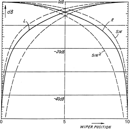
To give smooth stereo panning without unwanted level changes, the panpot should theoretically have a sine/cosine characteristic, as shown in Figure 22.6; with this law, both signals are attenuated by 3 dB when the panpot is set centrally. This is because when listening to stereo over loudspeakers, the signals that sum at each ear are not correlated, and so with equal amplitude, the two signals give a result that is only 3 dB above the level of each of the components. The summation of two uncorrelated white noise sources to give a combined signal that is 3 dB and not 6 dB greater works on exactly the same principle. The sine/cosine law is therefore appropriate for stereo.
However, when you are listening in mono, such as via AM radio, the left and right signals have been summed when they are still in the electrical domain and therefore are in phase and sum together arithmetically. In this case, the pan law needs to be -6 dB down at the centre rather than -3 dB if level changes are to be avoided, so in this case, a sine-squared/cosine-squared law is required. Since it is highly desirable to cope with both cases, the standard answer is to use a compromise between the two laws. This is entirely satisfactory in practice, not least because moving a component of the mix around during the performance is completely inappropriate for most forms of music, and I have yet to hear a music reviewer complain of “bad panpotting”.

Figure 22.6 shows both the sine and sine-squared theoretical laws, and also the lines L, R, which indicate the ideal compromise law; it is the arithmetical mean of sine and sine-squared and so is -4.5 dB down with the panpot central. So how do we obtain the compromise law we want?
Passive Panpots
Figure 22.7 shows three different ways to make a panpot. Panpot circuits can be made with single pots with the wiper grounded, as shown in Figure 22.7a, but this has several disadvantages, not least the poor offness when panned hard over, caused by the current flowing through the wiper contact resistance to ground.

Potentiometers with an accurate sine/cosine law used to exist, which in theory allowed the use of the simple panpot circuit in Figure 22.7b, but they were always bulky and prohibitively expensive for audio use and seem to have disappeared altogether now that analogue computers are no longer at the cutting edge of technology. Hi-fi preamplifiers sometimes use a control with a “balance law” for adjusting channel balance (see Chapter 14 for more on that), but this usually has no attenuation at all at the centre point and would make a poor panpot.
Figure 22.8 A panpot with law-bending resistors; unbuffered and buffered.
The traditional answer to the problem has always been to use dual linear pots and bend the linear law into an approximation of the compromise law we want by the use of fixed pull-up resistors connected to the wipers, as shown in Figure 22.7c. Here the panpot wipers are loaded with mix resistors of 10 kΩ, which being connected to virtual-earth buses are connected to ground as far as the panpot is concerned, and the pull-up resistors Rlaw are made 3k9 to give the desired 4.5 dB of attenuation at the centre position of the panpot.
There is an important factor in the design of panpot circuitry, and here a significant difference between low-cost and high-cost mixers intrudes. A low-cost mixer will drive the routing resistors directly from the panpot wipers, as shown in Figure 22.8a, and the panpot law is affected by the loading to ground represented by the routing resistors; they work in opposition to the law-bending pull-up resistors, which therefore have to be reduced in value (here to 3k3) to get the midpoint attenuation back to -4.5 dB. As the wiper loading increases and the value of the pull-up resistors is decreased with respect to the panpot track, the more the resulting law tends to flatten out around the central position, as shown in Figure 22.9. Table 22.1 shows how the law-bend resistors change with loading when a 10 kΩ pot is used, and the resulting pan laws can be seen in Figures 22.9 and 22.10.
The distorted law that results from excessive loading gives a panpot that does little as it is moved through the central position and has an unpleasant “dead” feeling; there are also level problems, as previously described. In addition, the lower the pull-up resistors, the greater loading they place on the stage upstream, which is usually the fader post amp; the loading is at its worst when the panpot is hard over to either side. This way of using a panpot presents a compromise on top of a compromise and puts a limit on the number of mix resistors that can be driven directly from a panpot.
Figure 22.10 shows the differences between the ideal compromise law and the actual law that results from law bending for various wiper loadings as in Table 22.1. The amplitude error of the right output gets enormous as the loading increases; when the panpot begins to move away from hard left, the level shoots up much too quickly.
Since the value of the pull-up resistor required to get the best approach to the required law depends on the loading on the panpot wiper, this is a very good reason to use routing methods that place a constant load on the panpot, regardless of the number of buses that are being routed to, as this at least allows the value of the law-bending resistors to be optimised at one value. More on this later.
| Trace in Figures 22.9, 22.10 | Wiper loading | Pull-up resistor |
|---|---|---|
| 1 | 15k | 5k |
| 2 | 4k | 2.2k |
| 3 | 3k | 1.8k |
| 4 | 2k | 1.2k |

Figure 22.9 How the law of a panpot varies with loading on the wipers; in each case, the law-bending resistors have been adjusted to give -4.5 dB at the centre. See Table 22.1.
A more sophisticated approach is used in high-cost mixers, which puts unity-gain (or near-unity-gain) buffers between the panpot and the loading of the routing resistors, as shown in Figure 22.8b. Here there are two points to note: the panpot wipers now have a negligible loading to ground, and the pull-up resistors therefore have a much higher value of 10 kΩ, which will improve offness as less current goes through the wiper contact resistance. Also, the routing resistor values can be reduced, as they no longer load the panpot, and this reduces the Johnson noise generated in the summing system.
This law-bending technique is a workable solution and has been very widely used, but unfortunately, the addition of the law-bending resistor introduces another problem. A reasonable-quality pot has an offness of about -90 dB with reference to fully up due to the end-of-track resistance. The pull-up current from the law-bend resistors, however, passes through the wiper contact resistance, which is usually greater than the end-of-track resistance, and this extra resistance severely limits the attenuation the panpot can provide when set hard left or right, degrading the offness of the panpot from approximately -90 dB to -65 dB when it is hard over. The problem is made worse because when the wiper is at the bottom of the track, the whole of the signal voltage across the pot is also across the law-bend resistor, which is lower in resistance than the pot track and so passes more current through the wiper contact resistance. The exact value of offness obtained depends on the component values and the construction of the pot. The way this works is shown in Figure 22.11.

Figure 22.10 The difference between the ideal compromise law and the actual law that results from law bending. See Table 22.1.
This reduction in offness is not really a problem in stereo use, as an attenuation of -65 dB is more than enough to pan a sound so it is subjectively completely to one side (in fact, about -20 dB will do that), but it is a very serious issue for mixers that route to groups in pairs, or in other words have one switch to route to Groups 1 and 2, another switch for Groups 3 and 4, and so on. Simpler mixers route to groups in pairs, as this makes good use of two-changeover switches (and, as mentioned before, the channels are by a long way the most cost-sensitive part of a mixer), but it means that if you are, say, routing to Group 1 by pressing the 1–2 switch and then panning hard left, then the signal being sent to Group 2 will only be -65 dB down. In bigger and more expensive consoles, each group has its own routing switch, with the spare switch section typically used for an indicator LED, so panpot offness is not such an important issue.
The Active Panpot
I think that it has been made clear that a conventional panpot is a bundle of compromises, and I decided in 1989 to do something about it. The Active Panpot was one of those ideas that strikes with such force that you remember exactly where and when it happened: in this case on the fifth floor of a tower block in Walthamstow, London. I had a glass of beer in my hand and had consumed half a pint. Ideas often strike at that point, but seldom after.
The active panpot shown in Figure 22.12 works by replacing the simple pull-up resistor with a negative-impedance-converter that modulates the law-bending effect in accordance with the panpot setting, making a closer approach to the sine law possible. This sounds intimidating but is actually very simple. The wiper of the left half of the panpot is connected to a series-feedback amplifier U1:A that gives a modest gain of about 2 dB, set by R2 and R3; the exact value shown in Figure 22.12 is 1.73 dB. The law-bending resistor R1 is driven from the output of this amplifier rather than the top of the panpot, and so, when the panpot wiper is at the lower end of its travel, there is little or no signal to the amplifier and therefore no pull-up action when it is not required. There is therefore no signal current flowing through the wiper contact resistance, so the left-right isolation using a good-quality pot is greatly improved from approximately-65 dB to -90 dB, being now limited solely by the end-of-track resistance as shown earlier in Figure 22.11a. As an extra benefit, if the amplifier gain and the law-bend resistor are correctly chosen, the pan law is much closer to the desired sin/sin2 compromise law than can be obtained by the simple law-bending method described; this is illustrated in Figure 22.13. This concept was protected by patent number GB 2214372 in 1989.

Figure 22.11 How the law-bending resistors degrade the offness of a panpot.

Figure 22.12 The active panpot: the law-bend resistor is driven from an amplifier stage with a gain of about 2 dB.
The active panpot is obviously a more expensive solution, as we have added a dual opamp and four resistors to every channel. However, we get other benefits for our money as well as better pan offness and a better pan law; if the dual opamp is a 5532 (which it should be to keep the post-fade noise down), then its good drive capability means that the value of the routing resistors can be reduced, which reduces both capacitive crosstalk and noise in the summing system.
LCR Panpots
A relatively recent innovation in the world of panpots is the LCR panpot, where LCR stands for left-centre-right. This has three outputs; the left and right in general working the same way as for a normal panpot. As the panpot is moved from extreme left, the centre output rises from zero, reaches a maximum with the panpot central, and then falls to zero again as the panpot reaches extreme right. The LCR panpot is used with speaker systems that have a central cluster as well as left and right speaker banks. This means that centrally panned signals are always heard as in the centre of the sound field, regardless of listening position, and this is useful when vocals or speech are combined with music, as typically occurs in religious installations. It is also used for panning to a discrete centre channel to create Surround and 5.1 mixes. A switch is normally provided by which the LCR pot can be converted to conventional L/R stereo operation.
There are two possible ways to handle LCR panning. In what I call the “full-width” method, as shown in Figure 22.14, the left and right panpot outputs work much as they do in a normal stereo panpot, only falling to zero at the extreme end of control rotation.

Figure 22.14 A full-width LCR panpot law. Left and right cross over at -4.5 dB in the centre as before, while C is 0 dB at the centre but zero at each extreme.
The alternative is the “half-width” method in which both left and right outputs fall to zero at the centre setting and stay there for further control rotation; this is shown in Figure 22.15. Both figures show laws which are a sin/sin2 compromise as described earlier and are therefore 4.5 dB down at the centre –in the case of the half-width method, these “centres” are at pot positions of 25% and 75% rotation. Which LCR panning method is most appropriate depends on the application; some LCR panpot systems can switch between the full-width and half-width modes.
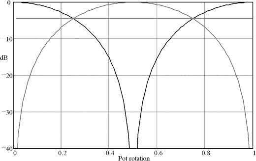
Figure 22.15 A half-width LCR panpot law. Left and right fall to zero at the centre setting and stay there for further control rotation. The crossover points between left and centre and right and centre are now at -4.5 dB.
Figure 22.16 shows a full-width LCR panpot arrangement. The L and R sections are as for a normal L-R panpot, but the C pot track is grounded at each end and fed with signal via its centre-tap; an LCR panpot always requires specially designed pots with centre-taps on the tracks. These are available from major manufacturers like Alps, but they are inevitably made in small quantities and are relatively expensive.
Figure 22.17 shows a half-width LCR panpot. The L and R sections now are also centre-tapped (more expense!), and those taps are grounded so that the output falls to zero at the central control setting. The C pot track is grounded at both ends and fed with signal via its centre-tap as before.
Figure 22.17 A half-width LCR panpot system. The L and R sections are now centre-tapped also.
LCR panpots, like ordinary panpots, give much superior performance in terms of offness and a better pan law when the active panpot system is applied to them. This is straightforward to do and is arranged exactly as for the stereo version.
Consoles with LCR panning systems include the Soundcraft Series 5, the Yamaha M2500–56, the D&R Orion, and the Amek 9098i. True LCR panning is not common, as it is a relatively high-cost facility.
Routing Systems
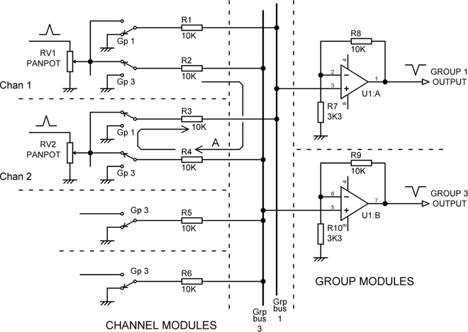
The routing system selects which mix bus the channel signal goes to. In a simple N into 2 stereo mixer the panpot does all the routing that is required, but as soon as more groups are introduced some sort of switching is required for bus selection.
Figure 22.18a shows the conventional routing system as commonly used up until about 1980. There are two problems with this method. First, the capacitance between the switch contacts when they are open is significant, and this severely limits the crosstalk performance of the console. To get a feel for the problem, look at Figure 22.19, which shows the crosstalk performance of an ALPS SPUN two-changeover switch working into a mix bus with a 10 kΩ feedback resistor in the summing stage. This is a conventional push-switch with two parallel sections.
At 10 kHz, the offness is only -66 dB, and at 20 kHz it is barely -60 dB. The problem is capacitive crosstalk across the switch contacts in the off position. Note that grounding the second switch section in the pious hope of improving things only reduces the crosstalk by 2 dB.
Figure 22.18 Two mediocre routing systems with virtual-earth summing, as used in the 1970s; a) suffers from poor offness and b) has bad noise performance.

This problem can be completely eliminated by using the arrangement in Figure 22.18b, which is sometimes called the back-grounding system. The mix resistors are now connected to the channel ground when not in use, and so there is no possibility of capacitive crosstalk, so long as the switches, of which one contact still carries signal voltage, are not too close to the mix buses. But … this plan has a terrible drawback. The crosstalk performance is good, but back-grounding the mix resistors means that since relatively few routing switches are on at a time, most of the resistors are grounded, and the summing amp is working at or near maximum noise gain and always picks up the maximum possible ground noise.
It might be wise to take a moment here to explain the noise gain of a summing system; noise gain itself is dealt with in Chapter 1. A simple inverting amplifier with equal input and feedback resistors has a noise gain of two times, or 6 dB, because the noise referred to the amplifier input sees effectively a non-inverting amplifier with a gain of two, and so the noise at the output is twice that of the noise-generating mechanisms at the amplifier input. The important point is that the noise gain is greater than the signal gain, which is unity.
If a second mix resistor of equal value is connected to the summing point, the amplifier input now sees effectively a non-inverting amplifier with a gain of three, and the noise gain is increased to almost 10 dB, though the signal gain via either mix resistor remains unity. The more channels that are routed to a mix bus, the worse the noise performance is, as summarised in Table 22.2. It is therefore clear that the arrangement in Figure 22.18b will be working at the worst-case noise gain all the time. Not only will the noise of the summing amp receive maximum amplification, but any ground noise in the console which puts the channel grounds at slightly different potentials will be picked up as effectively as possible. This is not a good plan, especially in large consoles.
Obviously a routing system that combined the advantages of the first two systems –good offness and minimum noise gain –would be a great improvement.
So, finally, here is the most satisfactory routing system. In the arrangement shown in Figure 22.20, the routing resistors are once more grounded when not being fed by the channel, but the topology has been turned around so that the grounded resistors are now connected to the channel rather than the mix bus. The switches rather than the routing resistors are connected directly to the summing buses, and when a routing switch is not active, the feed from the routing resistor is grounded. So long as the hot end of the mix resistor can be kept away from the mix buses, the offness is truly excellent. With a bit of care in the physical construction, the offness can easily be better than -100 dB at 20 kHz. A possible objection is that all the grounded resistors put a heavier load on the channel circuitry upstream; this is quite true, but it has the countervailing advantage that since each mix resistor is either grounded directly or connected to a virtual-earth mix bus, the loading remains constant, and so if, for example, the resistors are driven from an unbuffered panpot, you will get a predictable panning law, if not necessarily a very good one. This routing method retains the advantage of working the summing system at the minimum noise gain.
| Number of mix resistors
|
Noise gain | Noise gain |
|---|---|---|
| times | dB | |
| 1 | 2 | 6.02 |
| 2 | 3 | 9.54 |
| 4 | 5 | 13.98 |
| 8 | 9 | 19.08 |
| 12 | 13 | 22.28 |
| 16 | 17 | 24.61 |
| 24 | 25 | 27.96 |
| 32 | 33 | 30.37 |
| 48 | 49 | 33.80 |
| 56 | 57 | 35.12 |
| 64 | 65 | 36.26 |

Figure 22.20 The routing system that I introduced in 1979, which gives both good routing offness and optimal noise performance. Virtual-earth summing system also shown.
I have a difficulty here. To the best of my knowledge, I invented this system in the backroom of a shop in Leyton, London, in 1979. I recall being nervous about the apparently iffy business of having the routing switch at virtual earth because of increased stray capacitance to ground from the virtual-earth bus, but in fact that caused no problems. However, since very little has been published about the details of mixer design, it being a proprietary art confined to a relatively small number of companies, it is not currently possible to say if I was the first to invent it.
The set of routing switches in each channel (often called the routing matrix) is relatively expensive and is of course multiplied by the number of channels. It is therefore common on all but the most expensive consoles for routing to be done in pairs; in other words, the first switch routes the channel to Groups 1 and 2, the second to Groups 3 and 4, and so on. This is simple to do, as many varieties of push-switch come in a two-changeover format as standard. If routing to only one group is required, then the signal has to be steered to the appropriate bus with the panpot. The offness of the panpot when set hard over is then crucial to obtaining good crosstalk figures; the active panpot scheme described greatly improves this aspect of performance.
This system solves the electrical problems, but it relies on there being adequate physical separation between conductors carrying signal and the mix buses, to keep the capacitance between them low. This can present some interesting topological challenges. The obvious way to arrange the routing matrix is to put the switches next to the front panel, with the mix resistors behind them. Assuming we are using a double-sided PCB, the tracks from the panpot to the mix resistors are on the other side of the board from the mix buses, but inevitably they have to cross over at some point, separated only by fibreglass. Back in the dark days when the cost penalty of double-sided PCBs was very serious, a single-sided PCB would be used with various convolutions of tracks and topside links used to get signals to the right places; this was inevitably a bundle of crosstalk compromises. Even a double-sided layout falls a long way short of perfection, as there is no screening between the panpot tracks and the mix bus tracks at the point where they cross. Keeping the track width to a minimum at this point reduces the capacitance between the tracks, but it remains the major limitation on crosstalk, i.e. “routing offness”. If the routing resistors are through-hole, the pads and component leads on the same PCB side as the mix buses will also contribute to unwanted coupling.
The solution to this problem, introduced by me in the Series 6000 in 1987 at Soundcraft, was to reduce the size of the routing resistors from 1/4W to 1/8W, which made them small enough to fit between the actuators of the routing switches, right at the front edge of the PCB. This placed the mix resistors well away from the rear of the switches, which was the furthest extent of the mix buses, and likewise the panpot tracks could be run along the very front of the PCB. The use of a double-sided PCB allowed a ground plane to be placed on the other side of the mix buses. This form of construction was very successful, giving a major improvement in routing offness, and was later used in the famous 3200 console in 1988. Nowadays, the mix resistors would probably be metal-film SMD and could be fitted in very tight spaces at the front of the routing switches.
Auxiliary Sends
These are straightforward. There is often a pre/post switch before the send pot so the send signal can be taken from before or after the fader. In many designs, added flexibility is given in the form of push-on links so that other take-off points for the send signal can be used, such as before the EQ section. Changing all these links on a large console is naturally not a light matter.
If there is an on/off switch for the send, then it should disconnect the mix resistor from the bus, just as with the group routing switches described earlier. This reduces summing noise dramatically if only a few auxes are in use and gives an offness much better than that at the end of the aux pot travel.
Group Module Circuit Blocks
Most of the circuit blocks used in group modules carry out the same functions as they do in the input channel modules. The great exception is of course the summing amplifier, which has a technology all its own. Before diving into the details of practical summing amplifiers, it is advantageous to look at the various methods of performing that apparently simple but actually rather demanding task: adding signals together. The most fundamental function of a mixer, as its name suggests, is to combine two or more signals in the desired proportion. As with many areas of electronics, an extremely simple definition of the job to be done (addition: how hard can that be?) rapidly shows itself to have ever-deeper levels of complexity.
There are several intriguing techniques to look at:
- • Voltage summing
- • Virtual-earth summing
- • Balanced summing
- • Ground-cancel summing
- • Distributed summing
Summing Systems: Voltage Summing
The earliest mixers used voltage summing, or passive summing as it is sometimes called, as shown in Figure 22.21; note that only half of each panpot is shown for clarity. The great drawback with this system is that there is a significant voltage on the mix buses, so that a signal can be fed onto the bus by one channel, and it can get back into another channel, as shown in the figure, from where it may, depending on the control settings, find its way onto another mix bus where it is definitely not wanted. This is demonstrated by the arrow A in the diagram. Channel 1 is feeding a signal onto Group 3 bus, and this is sidling back into Channel 2, which has both routing switches engaged and the panpot central, allowing the signal to turn round and get onto Group 1 bus. This sort of thing can of course be completely suppressed by suitable buffer stages after the panpot, and that is exactly what was done in the large consoles of the day. This means a lot of extra electronics, and this mixing system is not suitable for low- or medium-cost designs. Another big snag is that since the mix buses have significant voltages on them, they must be carefully and expensively screened from each other to prevent capacitive crosstalk. Running the buses in a piece of low-cost ribbon cable is simply not an option.
You will have noted that all the routing switches are back-grounded, so there is a constant impedance from the mix bus to ground; this is essential, as otherwise the gain of the summing system would vary with the number of channels routed to a bus. This in turn means that the amplifiers that get the low level on the bus back up to the nominal internal level are working at substantial gain and are relatively noisy.
Summing Systems: Virtual-Earth Summing
Summing today is done almost universally by virtual-earth techniques, as shown in Figure 22.20. An opamp or equivalent amplifier with shunt feedback is used to hold a long mixing bus at apparent ground, generating a sort of audio black hole; signals fed into this via mixing resistors apparently vanish, only to reappear at the output of the summing amplifier, as they have been summed in the form of current. The great elegance of virtual-earth mixing, as opposed to the voltage-mode summing technique in Figure 22.21, is that signals cannot be fed back out of the bus to unwanted places, as it is effectively grounded, and this can save massive numbers of buffer amplifiers in the input channels. The near-zero bus impedance also means that the gain does not alter as varying numbers of channels are routed to a bus. The appearance of the virtual-earth mixing concept was highly significant, as it essentially made low-cost mixing consoles viable.
There is, however, danger in being dazzled by this elegance into assuming that a virtual earth is a perfect earth; it is not. A typical opamp-based summing amp loses open-loop gain as frequency increases, making the inverting input null less effective. The “bus residual” (i.e. the voltage measurable on the summing bus) therefore increases with frequency and can cause inter-bus crosstalk in the classic situation with adjacent buses running down an IDC cable.
As we saw in the last section on routing, a virtual-earth summing system operates at quite a high noise gain when many inputs are routed to it. Minimising the noise is therefore of prime importance, and one obvious step is to keep the impedance of the summing system as low as possible to reduce Johnson noise in the mix resistors. I have been involved in more mixing console designs than I care to contemplate, of all sizes and types, and it is interesting to recall that the mix resistors were always in the range 22 kΩ to 4.7 kΩ, which seems like a rather narrow range of 4.7 to 1. There is a reason for this. 22 kΩ mix resistors are used in small-budget consoles because a small number of them (say six) can be driven directly from a panpot without distorting its law unacceptably. Now consider a big expensive 32-group console where the panpot is buffered, but it has to drive 16 mix resistors on each side with the buffer, and making them of very low resistance would present enormous loading. The mix resistors will therefore be something like 6.8 kΩ; the value has only been reduced by a factor of 3.23, and Johnson noise will only be reduced by the square root of this, or 5.1 dB.
Mix resistors lower than this are only used for the critical L-R mix buses, where there are only two to be driven, and 4.7 kΩ is a common value. It actually only gives an advantage of 1.6 dB over 6.8 kΩ. The lowest mixing resistors I am aware of are in fact 4.7 kΩ, and this value was used in the Neve VR consoles, which in their largest formats had a possible 144 inputs going to the L-R mix bus (72 modules each with two paths to the mix bus).
This consideration of resistance demonstrates the difficulty of reducing the Johnson noise beyond a certain point by reducing the summing impedance. Halving the mix resistors doubles the drive power required but only improves the noise by a factor of the square root of 2. Johnson noise is of course only one factor; there is also the noise from the summing amplifier itself. The current-noise component of this is reduced proportionally by reducing the bus impedance.
Apart from the noise performance, another advantage of a low summing system impedance is that it makes the mix buses less sensitive to capacitive crosstalk. Reducing mix resistors from 22 kΩ to 6.8 kΩ may only give a 5.1 dB improvement in noise, but it gives a 10 dB reduction in capacitive crosstalk.
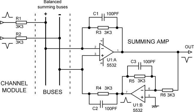
Balanced Summing Systems
As a console grows larger, the mix bus system becomes more extensive and therefore more liable to pick up internal capacitive crosstalk or external magnetic fields; the latter are poorly screened by the average piece of sheet steel. The increased physical size means longer ground paths with non-negligible signal voltage drops across them. An expensive but thoroughly effective answer to this is the use of a balanced summing system. The basic idea is shown in Figure 22.22; only half of the channel panpot is shown for clarity.

Each mix bus is now double, having a hot (in-phase) and cold (out-of-phase) bus, exactly like the hot and cold wires in a balanced line connection. These run physically as close together as possible. At the channel end, each side of the panpot has an inverting buffer A2 that drives a second set of mix resistors that feed the cold mix buses. Two sections are now required for the routing switch SW1, which is fine, as most push switches are in a two-changeover format, but if you want switch status indication, which you normally will on a console large and sophisticated enough to employ balanced summing, four-changeover switches are needed – lots of them – and the cost jumps up. Each bus connects to a summing amplifier A3, A4, and their outputs are subtracted by A5 to cancel the common-mode signals.
A quite separate advantage of a balanced summing system is that it has a better noise performance, because having two buses gives you 6 dB more signal but only 3 dB more noise, because the noise from the two summing amplifiers is uncorrelated and partially cancels. This gives you a 3 dB noise advantage that it would be difficult to get by other methods. Against this must be counted the extra noise from the channel inverters.
Because of the cancellation of capacitive crosstalk that occurs, the offness of the routing matrix can be made very good indeed. On the last console of this type that I designed, the offness was a barely measurable -120 dB at 20 kHz.
As I just noted, probably all consoles of this type will have routing switch status indication and so use four-changeover switches. This leaves a spare switch section doing nothing, and if you have followed this book so far, you will have gathered it is not in my nature to leave a situation like that alone. In the last balanced console I designed, this fourth switch section was used to detect when no routing switches were active; this happens more often than you might think on a large desk. In this condition, an FET switcher removed the signal feed to the buffers driving the mix resistors. This prevented a large number of grounded resistors being pointlessly driven, reducing power consumption significantly, and further improving routing offness.
It may have occurred to you that a considerable simplification would result if the channel inverters were done away with and the cold resistors simply connected to ground. The signal level in the summing system would be 6 dB lower, exacting a 3 dB noise penalty, but the rejection of ground voltages and the cancellation of capacitive crosstalk would be just as good. This is not a sound plan. Much of the cost of balanced summing lies in the doubled number of mix resistors, routing switch contacts, and mix buses. The saving on inverter cost is relatively small. The large currents flowing in the mix resistors are now unbalanced and are much more likely to cause troublesome voltage drops in ground connections.
A variation on this approach can, however, be very useful in specific applications; see the section on ground-cancel summing systems.
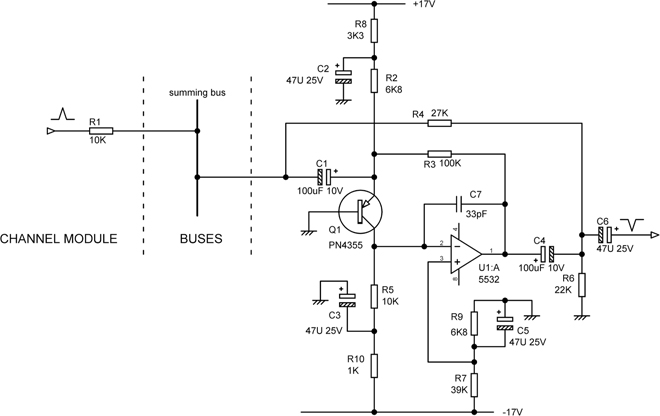
Ground-Cancelling Summing Systems
Ground-cancel summing systems are very useful in auxiliary send systems where all sends are routed permanently to the bus. It gives some of the advantages of a balanced summing system at a tiny fraction of the cost, and it is particularly useful in consoles where the modules are connected together by ribbon cabling with a relatively high ground resistance. The basic principle is shown in Figure 22.23, which represents a single channel with two aux sends. The ground potential of each channel is read by a low-value resistor R3 and summed into the GC bus; this is not a virtual-earth bus as such, but it is at a very low impedance and is essentially immune to capacitive crosstalk. The GC bus is then used as the ground reference for the aux summing system, and by subtraction, it gives excellent rejection of the channel ground potentials. If a channel is at the remote end of the ribbon cable, then its ground resistance is relatively high and the local channel ground will carry a large signal potential, which is fed into the GC bus; conversely, a channel at the near end of the ribbon cable will have a much lower ground potential, also fed into the GC bus. The end result is that good aux offness figures are obtained for both those channels. In such a system, the aux offness is defined not by the grounding arrangements but by the offness of the aux send pot itself, typically -90 dB with reference to fully up.
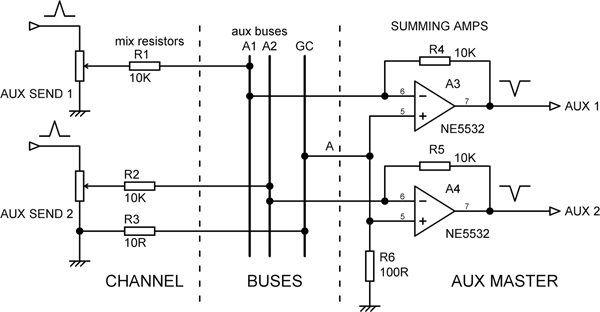
Figure 22.23 A typical ground-cancelling summing system for aux sends.
A couple of design points. The GC resistors R3 should be very low in value so that their Johnson noise contribution is negligible; the only requirement is that they are large with respect to the ground resistances to allow accurate subtraction. R6 is a safety resistor fitted in the aux master module so that it will keep working if the GC bus becomes disconnected. Without it, the entire aux send system is dependent on the single connection A between the bus structure and the aux master module, and such a situation is not good practice. The only requirement is that R6 is high with respect to the total GC bus impedance so that the subtraction remains accurate. If an aux send has an on/off switch that disconnects the mix resistor from the bus, to minimise noise gain, the switch must also disconnect the GC resistor to maintain correct cancellation.
In some ribbon-cable consoles, the grounding is reinforced by heavy (32/02) ground wires with push-on connectors plugged into every channel module, or in some cases every fourth or fifth module. Even in this case, the use of a ground-cancel summing system will normally give a worthwhile improvement.
Distributed Summing Systems
Distributed summing (sometimes called devolved summing or devolved mixing) is a deeply cunning way of improving the noise performance of a summing system, with reference to the noise from the summing amps themselves. In what follows, the noise from an input channel and Johnson noise from the summing resistors are, for the time being, ignored.
In a distributed summing system the contributory signals are summed in two separate stages. Thus if you are summing together 24 channels, you might sum them in blocks of 8 to get three sub-groups, which are then summed together to get a single output, as shown in Figure 22.24a. Unlikely as it may seem, this two-layer summing system gives a definite noise advantage. Assume that every summing amplifier creates the same amount of input-referred voltage noise Vn; the result of this at the amplifier output then depends on only the noise gain at which it is working. If we sum our 24 channels into one in the normal virtual-earth manner, the output noise will be 25 Vn, and that is our reference case. If we sum eight inputs together, the output noise will be only 9 Vn; three of these sub-mix outputs are now summed together, and – you may have seen this coming –the signals sum arithmetically but the summing amp noise partially cancels, so the combined noise output is 9 Vn times √3, which is 15.6 Vn. To this we must add the noise of our second summing amp; this is working at a noise gain of only 4, and so its own output noise contribution is 4 Vn. Adding the uncorrelated 15.6 Vn to 4 Vn rms-fashion gives a total of 16.1 Vn, which is 1.55 times or 3.83 dB quieter than the straightforward all-in-one-go summation of 24 inputs into one. Clever, eh?
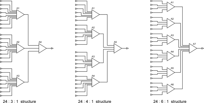
Figure 22.24 Three different distributed summing schemes for 24 inputs. 24:6:1 is the quietest.
The downside to this is of course that a bit more hardware is required –we are using four summing amplifiers rather than one. This is, however, a trivial extra expense compared with the electronics involved in 24 input channels. A more serious potential problem with this approach is that there is now a hidden layer of summing amplifiers which might clip without there being any indication on the console control surface.
You are by now, I hope, pondering if there is anything special about the 24 into 3 into 1 (24:3:1) structure or whether other variations might be better; the answer is yes. Three different possibilities are shown in Figure 22.24. Summing the 24 inputs in batches of six into four sub-mixes and then summing them to one (24:4:1) gives an advantage of 4.51 dB, while summing four at a time into six sub-mixes and then summing to one (24:6:1) gives an advantage of 4.97 dB, and this is the optimal solution for 24 inputs.
The results are summarised in Table 22.3, which shows that there is not much difference between 24:6:1 and 24:8:1, except that the latter uses a bit more hardware and is a negligible 0.2 dB noisier. It is hard to see why anyone would want to use the 24:12:1 structure because of all those extra summing amps, but it is interesting to note that it still gives a theoretical noise improvement of 3.53 dB.
Table 22.4 illustrates the noise advantages with various forms of two-layer summing for 32 inputs; the maximum advantage is now a very useful 5.88 dB, and once again, the best results come from first summing the inputs in batches of four. There are fewer options this time because 32 has less factors than 24.
| No. of inputs | No. of sub-mixes | Noise advantage dB |
|---|---|---|
| 24 | 2 | 2.56 |
| 24 | 3 | 3.83 |
| 24 | 4 | 4.51 |
| 24 | 6 | 4.97 |
| 24 | 8 | 4.76 |
| 24 | 12 | 3.53 |
| No. of inputs | No. of sub-mixes | Noise advantage dB |
|---|---|---|
| 32 | 2 | 2.68 |
| 32 | 4 | 4.94 |
| 32 | 8 | 5.88 |
| 32 | 16 | 4.01 |
Table 22.5 shows the optimal structures giving minimum noise for various numbers of inputs; at first, it looks as if there is something special about doing the first layer of summing in batches of four inputs, but as the total number of inputs reaches 72, the optimal number suddenly starts to rise.
The figures in Table 22.5 do show a rather unsettling irregularity; for example, the optimal structure for 80 inputs is no quieter than that for 72 inputs. This seems to be because some numbers of inputs have more factors than others and so give a greater choice of structures to choose from.
Two-layer distributed summing is particularly adapted to consoles built in sections, typically as bins of 8 or 12 modules. It avoids virtual-earth busses extending over large physical areas, which makes them more susceptible to magnetic fields and ground voltage-drops, and can cause difficulties with HF stability. Each bin can now be connected by balanced low-impedance line connections, with the final summing done at whatever point is convenient. Both Neve and Focusrite have produced consoles with distributed summing systems in the past.
As I’m sure you have appreciated by now, I am a great one for following a train of thought until it derails at the points and scatters passengers all over the track. If two layers of distributed summing give a better noise performance, would three layers be even better? The answer is generally yes, but not by much; basically, it’s not worth it. For example, the optimal two-layer structure 24:6:1 gives a noise advantage of 4.97 dB, while the optimal three-layer structure 24:8:2:1 gives 5.24 dB; the improvement over two-layer summing is a very small 0.27 dB. Noise performance is actually very slightly worse for the 16-input case, because you have added more summing amps creating noise without enough partial-cancellation going on to outweigh that.
| Total no. of inputs | No. of inputs in each sub-mix | Optimal structure | Noise advantage dB |
|---|---|---|---|
| 16 | 4 | 16:4:1 | 3.64 |
| 24 | 4 | 24:6:1 | 4.97 |
| 32 | 4 | 32:8:1 | 5.88 |
| 48 | 4 | 48:12:1 | 7.09 |
| 56 | 4 | 56:14:1 | 7.52 |
| 64 | 4 | 64:16:4 | 7.88 |
| 72 | 6 | 72:12:1 | 8.48 |
| 80 | 8 | 80:10:1 | 8.48 |
| 88 | 8 | 88:11:1 | 8.84 |
| 96 | 6 | 96:16:1 | 9.43 |
| 104 | 8 | 104:13:1 | 9.46 |
| 112 | 8 | 112:14:1 | 9.73 |
| 120 | 6 | 120:20:1 | 10.13 |
| 128 | 8 | 128:16:1 | 10.21 |
| 136 | 8 | 136:17:1 | 10.43 |
| 144 | 6 | 144:24:1 | 10.67 |
| Total no. of inputs | Optimal structure | Noise advantage dB | Advantage over two-layer summing dB |
|---|---|---|---|
| 16 | 16:4:2:1 | 3.57 | –0.07 |
| 24 | 24:8:2:1 | 5.24 | 0.27 |
| 32 | 32:8:2:1 | 6.24 | 0.36 |
| 48 | 48:16:4:1 | 7.99 | 0.90 |
| 56 | 56:14:7:1 | 8.33 | 0.81 |
| 64 | 64:16:4:1 | 9.06 | 1.18 |
| 72 | 72:18:9:1 | 9.27 | 0.79 |
| 80 | 80:20:5:1 | 9.97 | 1.49 |
| 88 | 88:22:11:1 | 10.00 | 1.16 |
| 96 | 96:32:8:1 | 10.74 | 1.28 |
| 104 | 104:26:13:1 | 10.59 | 1.13 |
| 112 | 112:28:14:1 | 11.33 | 1.60 |
| 120 | 120:40:8:1 | 11.62 | 1.49 |
| 128 | 128:32:8:1 | 11.87 | 1.66 |
| 136 | 136:34:17:1 | 11.51 | 1.08 |
| 144 | 144:36:9:1 | 12.35 | 1.68 |
See Table 22.6 for the optimal three-layer structures and their results. (Note that in the three-layer structures, the second figure denotes the total number of first-layer summing amps rather than the number feeding each summing amp in the second layer.) The greatest advantage over two-layer distributed summing is 1.7 dB, and that is for a monster mixer with 144 paths to the mix bus; getting that improvement involves using 36 + 9 = 45 summing amplifiers, when the optimal two-layer process uses 24. That’s almost twice as many, and we must regretfully conclude that three-layer distributed summing is of marginal utility at best.
Four-layer summing, anyone? Probably not; you would need a quite enormous number of inputs to make such a structure even faintly worthwhile.
Summing Amplifiers
Figure 22.25 shows a practical summing amplifier circuit using a 5534/2 opamp; the accompanying insert send amplifier is included because it gives a good example of how the summing amp phase inversion needs to be corrected before the signal sees the outside world again, and it also demonstrates how to apply the “zero-impedance” approach to an inverting stage. As mentioned before, the summing amplifiers were one of the first places that 5534/2s appeared in mixers, because the potentially high noise gain makes their noise performance critical. The circuit is very straightforward, but there are a few points to watch. First, the DC-blocking capacitor C1 is essential to prevent the bias current of the 5534/2 from making the routing switches clicky. It needs to be bigger than it might at first appear, because the relevant LF time-constant is not C1 and the mix resistor R1 in the channel but C1 and the parallel combination of all the mix resistors going to that bus. Thus for the 22 kΩ mix resistors and 100 μF capacitor shown, if there are eight input channels, the LF -3 dB point will be at 0.59 Hz. Table 22.7 illustrates how this works, and you can see that in this case, 100 μF is large enough for even a big mixer. If lower values of mix resistor are used, then C1 must be scaled up proportionally.
| No. of mix resistors | Total mix res to bus | -3 dB frequency |
|---|---|---|
| 1 | 22kΩ | 0.072 Hz |
| 8 | 2.75kΩ | 0.59 Hz |
| 16 | 1.375kΩ | 1.18 Hz |
| 24 | 917Ω | 1.74 Hz |
| 32 | 687Ω | 2.33 Hz |
| 40 | 550Ω | 2.90 Hz |
| 48 | 458Ω | 3.44 Hz |
It may appear that C1 is still rather oversized for the job. This is not so. The signal in a mixing console passes through a large number of RC time-constants on its journey from input to output, and even if each one causes only a tiny roll-off at the LF end, the cumulative effect on the frequency will be substantial. It is therefore essential that each LF roll-off is well below the normal audio band. The same considerations apply to HF roll-offs. See Chapter 1.
There is also the important point that electrolytic capacitors distort with even small signal voltages across them, as described in Chapter 2, and so they must be much larger than might otherwise be required.
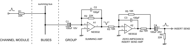
Figure 22.25 Simple opamp summing amplifier, followed by an inverting zero-impedance insert send amplifier that corrects the phase.
There is yet another reason to make C1 large. A summing amplifier aspires to appear as a short circuit to ground, and even if it is itself perfect, the presence of C1 means that the bus residual voltage will rise at low frequencies, possibly causing increased LF crosstalk.
The capacitor C2 across the summing amp feedback resistor R2 is another vital component; without it, the stage is pretty well guaranteed to be unstable at HF. This is because the mix bus has an appreciable capacitance to ground, and this will destabilise the opamp by adding an extra phase shift to the feedback through R2. Adding C2 compensates for this; its value is normally determined by experiment. It clearly must not be so large that it gives an excessive HF roll-off with R2.
A balanced summing system as in Figure 22.22 can easily be made using two separate summing amplifiers whose outputs are then subtracted. A more economical method which saves an opamp is shown in Figure 22.26; with equal resistor values, the overall gain is -6 dB. The downside is that it does not generate two true virtual earths. The two bus residuals are only low if symmetry holds in every part of the circuit, including the signal levels applied to the summing resistors. I built it with a 5532 and 1% resistors, and the bus residuals were both -61 dB (worsening above 1 kHz as usual due to opamp limitations). Changing either of the summing resistors or feedback resistors by 3% of their value increased this to -49 dB. Obviously these are not true virtual earths – more like virtual-virtual-earths. This method was used for the main mix bus in the Mackie Onyx mixer, among others.
Hybrid Summing Amplifiers
It is well known that at low source resistances, discrete bipolar transistors are normally quieter than opamps, the exception being specialised opamps like the AD797, which are usually ruled out on the grounds of cost. This applies to the normal run of low-cost transistors, though specialised types such as the 2SB737 are even better. While the advantage obtained varies with the number of summing resistors connected to the bus and their value, in general, a very desirable noise reduction of about 5 dB may be expected in a large console.
The hybrid combination of a discrete bipolar transistor input and an opamp to provide open-loop gain for linearisation and load-driving capability gives the arrangement shown in Figure 22.27. The summing bus is connected to the emitter of Q1 via the DC-blocking capacitor C1; the amplified signal from Q1 collector is passed to the opamp, which has a local feedback loop R3 which controls the DC conditions of Q1. The voltage set up on the non-inverting opamp input by bias network R7, R9, C5 determines the voltage at Q1 collector. C7 acts as a dominant-pole capacitor to give HF stability.
An outer layer of shunt feedback via R4 is used to minimise the effect of C1 in increasing the bus residual at LF by putting C1 inside this outer feedback loop. C4 prevents the non-zero voltage at the opamp output from getting onto the bus via R4, and in the same way, C6 is a DC blocking capacitor which prevents the following stage from putting any DC offset voltages on to the bus. This arrangement is effective at doing what it is supposed to, but there are clearly several LF time-constants involved because of the various blocking capacitors, and with such schemes, it is essential to check that there is no peaking or other irregularity in the frequency response at the bottom end.
While the one-transistor version gives a good noise performance, it is susceptible to rail noise getting into the emitter or collector circuits of the transistor, and very careful filtering and decoupling are required to prevent this putting a limit on the noise performance. Another potential problem is that there will be LF signal-related voltages on the supply rails due to the limited effectiveness of decoupling capacitors of reasonable size, and if these get into the summing amplifier, they will compromise the LF crosstalk performance. An excellent fix for these issues is the use of a two-transistor circuit as in Figure 22.28. The two transistors are used in a balanced configuration that cancels out rail noise and makes the decoupling requirements much simpler; there is also no need for a biasing network as in the one-transistor version.
There are one or two subtleties to be observed here; the shunt feedback must go to the same transistor as the VE bus to prevent large current swings in the transistors that would cause distortion. This means that the feedback must be inverted to be in the right phase, which is done by U1:B. This introduces stability-threatening extra phase shifts, so HF stability capacitor C4 bypasses the feedback inverter and goes straight to the emitter of Q2. A very useful property of this arrangement is that the output is in phase and so can be fed directly to a group insert.
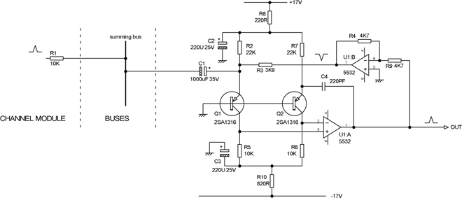
Figure 22.28 Two-transistor hybrid summing amplifier is better at rejecting noise and crosstalk from the supply rails.
A more sophisticated version of this summing amplifier, which I thought up a while ago, is shown in Figure 22.29. Here the aux master level control RV1 not only acts as a normal gain control but also alters the amount of negative feedback around the summing amplifier, effectively giving the stage variable gain. This can be extremely useful, as aux summing amplifiers often have large numbers of inputs feeding them and are more liable to clipping than group summing amplifiers. It is extremely tedious to turn down dozens of aux sends to remedy the situation, so being able to reduce the aux summing amp gain is advantageous.

Figure 22.29 Two-transistor hybrid summing amplifier with positive feedback to enhance gain at high control settings only, improving headroom at low gain settings.
When RV1 is at minimum, the circuit is essentially that of Figure 22.28, with the main shunt feedback path through the inverter U1:B, and the HF stabilising path through C7. The value of the main feedback resistor R3 is chosen so the sum amp gain is low, in this case -6.8 dB, so overload is unlikely. When RV1 is turned up, a positive feedback signal is sent to the non-inverting input of U1:B via R11 and R12, and the partial cancellation that results reduces the output of the inverter, decreasing the overall amount of negative feedback and increasing the gain of the summing amplifier. The need for a post amplifier with make-up gain is therefore avoided, improving the noise performance.
This technique was used in the Soundcraft Delta mixing console, and I modestly propose that it might be one reason why it won a British Design Award in 1991. My collaborator in the design of the Delta was Mr Gareth Connor. This technology was also used in the Soundcraft Venue-2 mixing console.
Balanced Hybrid Summing Amplifiers
In sophisticated consoles, it is desirable to combine the benefits of balanced mixing with low-noise hybrid summing amplifiers. The obvious method of implementing this is to use two hybrid summing amplifiers and then subtract the result, but this uses quite a lot of hardware. A more elegant approach is to use a single balanced hybrid summing amplifier to accept the two antiphase mix buses simultaneously; this reduces noise as well as minimising parts cost and power consumption.

Figure 22.30 Two-transistor balanced hybrid summing amplifier. Note the dual feedback paths via R3 and R12.
The circuit shown in Figure 22.30 is at first sight very similar to that in Figure 22.28, but with the crucial difference that two mix buses now feed into the stage, one to each transistor emitter. To prevent distortion-inducing variations in the transistor currents and to maintain symmetry, it is therefore now necessary to also apply shunt feedback to both transistor emitters. The feedback to Q1 is taken via an inverter to get the phase right, as in Figure 22.28, but the other feedback path is simply resistor R12. As before, C4 gives HF stabilisation.
Note that the configuration is very similar to that of the balanced microphone amplifier described in Chapter 17 and gives low noise as well as excellent symmetry. This technology was used extensively in the Soundcraft 3200 recording console; once again, my valued collaborator in the design of the 3200 was Mr Gareth Connor.
Balancing Tracks to Reduce Crosstalk
It is inherent in the two-transistor hybrid summing amplifiers described earlier, whether operated single-ended or balanced, that two anti-phase outputs are produced. There are also anti-phase inputs, though in single-ended operation, the non-inverting input is not used. The anti-phase outputs can be very handy if it saves putting another stage in just to get the phase right (something I always deprecate). However, this feature can be further exploited to reduce crosstalk within a module.
A virtual-earth bus is very susceptible to capacitive crosstalk, and its most vulnerable time is when it gets onto the module where its summing amplifier lives. A typical group, aux master, or mix master module will have much more circuitry on it, probably carrying unrelated signals we want to keep out of the mix buses. Physical separation helps, but on a crowded module, it may not be possible to get enough of it. Making the track as narrow as possible also helps because it reduces the capacitance through which signals can crosstalk, but this is of limited effectiveness.
A highly effective approach is to run a second track parallel to the incoming mix bus as close to it as the PCB design rules allow and starting where it comes onto the PCB. There is no connection the balancing track at this end, but the other end is connected to the non-inverting input of the summing amp, and any signal coupled to it is subtracted from the summing amp output signal. The effectiveness of the cancellation (which is exactly analogous to the common-mode rejection ratio of a balanced line input) depends on the details of the geometry of the crosstalk source(s) and the mix buses, on accurate feedback resistors in the summing amplifier, and on the balancing track being the same width as the mix bus track. There are too many variables for accurate predictions to be made, but it is straightforward to get a 20 dB improvement in crosstalk by this method.
Figure 22.31 shows a single-ended summing amplifier using both input and output balancing tracks. Note how the input balance track snuggles around the DC blocking cap C1.
Once our signal has been through the summing amplifier, it is at a very low impedance and is effectively immune to capacitive crosstalk, but now it has some voltage and so the potential to crosstalk to other virtual-earth buses and any other circuitry not at a low impedance. This can be much helped by running a balancing track from whichever of the anti-phase summing outputs is not in use. Once again, this parallels the summing amp output track, as close to it as possible, and has the same track width. Thus, to a large extent, signals radiated as an electric field from the output track are cancelled out. The exact amount of improvement depends on track geometry, etc., as for input balancing tracks.

Figure 22.31 Input and output balancing tracks applied to a two-transistor balanced hybrid summing amplifier.
Both balancing methods were used in the Soundcraft Sapphyre group module, to give just one example.
The Multi-Function Summing Amplifier
Figure 22.32 shows a summing amplifier that incorporates hybrid BJT-opamp technology, input and output balancing tracks, a zero-impedance output, and a ground-cancelling output, all in one stage. When people come up with a new idea, they often decide to throw in a number of other ill-advised ideas. Please don’t think that this is some sort of doubtful throw-it-all-in demonstration. Figure 22.32 is the actual summing amplifier used with great success in the Soundcraft Sapphyre mixer. Manufacture has long ceased, but Sapphyres are still changing hands for remarkable sums of money.
The zero-impedance feature is obtained by taking the audio-band negative feedback from the outside end of R11; the HF feedback goes directly through C4 from the inside end of R11 and gives stability in the face of capacitive loading on the output. The ground-cancelling feature is obtained by adding a ground-cancel input load resistor R13 and feeding the cancel signal back into the summing amp via R1, which, in conjunction with R8, gives unity gain and good cancellation. These features are simple to add and do not interact with each other.
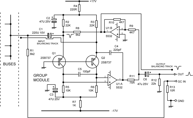
For more information on zero-impedance outputs and ground-cancelling outputs, see Chapter 19.
PFL Systems
The pre-fade listen (PFL) facility goes back a long way in the history of mixers, almost certainly first appearing on broadcast consoles, where it proved extremely useful to be able to listen to a source before unleashing it on an unsuspecting public. It is also very handy in a recording environment, allowing you to listen to one source in isolation without undoing dozens of routing switches. It is invaluable for checking the level in a channel; the PFL feed takes over the main Mix metering, which is usually much bigger and better than metering incorporated on a per-channel basis, if indeed there is any at all. On most mixers, there is only room for a Peak light. As the name suggests, a PFL feed is taken from before the fader so that the signal is heard at full level even if the fader is down. In the USA, it is often called the “solo” facility.
“PFL” is often used as a verb, as in “Could you PFL channel 23?” Interestingly, this request is always spelt out as P-F-L, and the obvious pronunciation as “piffle” has never achieved favour. When any PFL switch is pressed, a circuit block in the master section switches the left and right monitor outputs so they reproduce the PFL signal in mono, as shown in Figure 22.33. The L/R meters are also taken over by the PFL system so they can be used to check channel pre-fade levels, allowing the adjustment of input gain when required. It is common to switch both meters over, though of course they both read the same thing. Historically, the PFL switching was done with a relay, but this was taken over by electronic means, specifically 4016 analogue gates, at a relatively early date, as it is not essential for the switching to be absolutely click free. The later availability of discrete FETs designed for analogue switching improved the linearity and much reduced (but did not wholly eliminate) the switching transients.
All that is required on each channel is a switch section to route the pre-fade-signal to the PFL bus, which is a simple virtual-earth bus that works in the same way as group buses, and another switch section to signal via a PFL-detect bus that a switch has been pressed and the monitor source must be changed over. The PFL-detect bus simply gathers together all the signals that indicate a PFL switch is pressed; it does not have to be a virtual-earth bus, but there are advantages in making it so, as described in what follows. PFL switches are commonly fitted with indicator lights, even on quite small mixers, because otherwise it is necessary to hunt around the control surface if a PFL switch is inadvertently left pressed in. This does not make a third switch section (and therefore a four-changeover switch) necessary because the ingenious method shown in Figure 22.33 can be used. All the LEDS on a channel module are usually run in a chain from the positive to negative supply rails; so long as there are not too many LEDs, a simple series resistor is usually all that is needed to give more-or-less constant-current operation of the chain. If the PFL indicator LED is put at the top of the chain, SW1-A removes the short circuit from D1 and allows it to turn on, at the same time routing a DC signal into the PFL-detect bus via R1. (Note that the switch section SW-1B that routes the signal to the PFL bus uses the same high-offness configuration described earlier.)

This underlines the point that economy of design in a mixer channel is very important, because every extra component is multiplied by the number of channels. In the master section, the need to design out every possible component is less pressing.
PFL Summing
There is nothing very difficult about the PFL summing amplifier. It is not necessary for it to have the best possible noise performance, as it is only used for quick monitoring checks. The system shown in Figure 22.34 uses a dual opamp, the second half being used to restore the correct phase after the inversion produced by the summing amplifier. C1 provides DC blocking, while R2 keeps the PFL bus at 0 V DC to prevent switch-clicks. R3 sets the gain from channel to PFL summer as unity, and C2 prevents the bus capacitance from causing instability. R4 and R5 set the gain of the re-inverting stage to unity. C3 provides DC blocking at the output to prevent clicks when the PFL switcher operates.
PFL Switching
When the PFL system operates, the normal L-R mix is removed from the monitor outputs and is replaced by a mono feed from the PFL summing system. This is usually done by some form of electronic switching; see Chapter 21 on signal switching for more details.
PFL Detection
In early consoles a DC voltage was simply switched into a PFL-detect bus that operated the PFL switching relay directly. Moving that amount of current around inside a mixer is simply asking for trouble with clicks crosstalking into the summing buses, and very soon a transistor relay driver was added so the voltage and current levels on the PFL-detect bus could be much lower. When solid-state PFL switching was introduced, the transistor circuitry drove analogue gates or discrete FETs instead.
Two simple methods of PFL detection are shown in Figure 22.35. At 22.35a is demonstrated how not to do it. When the PFL switch SW1 is closed, +17 V is applied to the PFL-detect bus, turning on Q1 and illuminating the “PFL ACTIVE” LED D1 and turning Q2 off. The problem is that the 34 V edge on the PFL-detect bus (which normally sits at -17 V) has an excellent chance of crosstalking into the other summing buses.
A better method is shown in Figure 22.35b. Here the resistor R1 has moved to the channel module, and the PFL-detect bus connects directly to the base of the detect transistor Q1. This ensures that the PFL-detect bus can never change by more than 0.6 V, which reduces the possibility of clicks crosstalking capacitively into adjacent summing buses; there should be a 35 dB advantage. A countervailing disadvantage is that the base of Q1 is vulnerable to destruction if the PFL-detect line gets shorted to ground. It is also slightly more expensive to implement, as now there has to be a resistor R1 for each PFL switch.

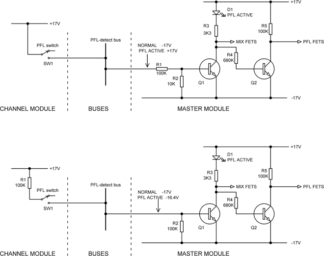
Figure 22.35 Two simple PFL-detect systems. The second version reduces the likelihood of clicks getting into other buses.
This method was workable when all mixers had mother boards, but the introduction of ribbon-cable interconnections between mixer modules put all the buses closer together and increased the likelihood of PFL-detect clicks becoming audible.
Virtual-Earth PFL Detection
The ideal PFL detection system would have no voltage edges on the detect bus at all. This can be done by detecting current instead of voltage –the PFL-detect line becomes a virtual-earth summing bus for DC signals. I thought this up in 1983.
Figure 22.36a shows the principle. U1 is simply a summing amplifier that works at DC. When no PFL switches are pressed, the output of U1:A sits at +10 V because the bias from resistor R2, Q1 is held on via R4, and Q2 is held off. Negative feedback through R3 keeps the detect bus at 0 V; C1 prevents the bus capacitance to ground from causing instability. The “PFL ACTIVE” LED has moved to the collector of Q2 to allow for the logical inversion caused by the summing amplifier. When a PFL switch is pressed, the current injected into the detect bus by R1 overcomes that from R2 and the output of U1 goes below 0 V, and Q1 turns off. Note that the signalling current is only 170 μA, so there is little possibility of inductive crosstalk. It could probably be significantly reduced without problems.
This simple version of the system will silently detect a single PFL button down but will come unstuck if more are pressed, because U1 output will hit the–V rail and will no longer be able to maintain a virtual earth on the detect bus. This situation is not uncommon, as it gives a rough submix of the channels pressed, and so it is wise to cater for any number of PFLs at once. The circuit of Figure 22.36a overcomes the problem by adding diode D1, which clamps the opamp output so that however many PFL switches are pressed, the opamp output will not hit the–V rail, and negative feedback will continue to keep the PFL-detect bus very close to zero volts. The values of R4 and R5 must be carefully chosen so that the level shift down to the–V rail works reliably, and Q1 will always switch correctly despite circuit tolerances.

Figure 22.36 Virtual-earth PFL-detect systems. The second version uses the PFL-detect bus to reset channel mute status at power-up.
Note that once again, all the circuitry works between the +V and –V rails, so there is no chance of transients being injected into the ground system.
This arrangement has another, less obvious advantage. It can handle signals in both directions. The ribbon-cable systems referred to earlier come in a number of fixed widths, so you can buy 40-way cable, but if you need 41 ways, the next size up is 50-way. Since this increases the cost not only the cable itself but of all the connectors on it and all the mating module connectors, increasing the cable size is not a decision taken lightly. In one mixer design, there was a need to send an initial-reset signal to mute-control flip-flops on each module, and all 40-ways of the ribbon cable were committed. The only way to avoid 50-way cabling was to make the PFL-detect bus dual-function.
The idea is that by changing the reference voltage applied to the PFL-detection opamp, you can change the DC voltage that it maintains on the detect bus. In Figure 22.36b, at power-up, the initial-reset network R9, R10, C2 pulls the reference voltage going to the non-inverting input of U1 low for a brief period until C2 fully charges, and the PFL-detect bus is therefore also pulled low via R3, and this signal is coupled to each channel mute-control flip-flop by a diode D3; the flip-flop works between positive and negative supply rails so it can drive muting FETs directly. After the initial-reset period, the PFL-detect bus settles at its normal level of 0 V, and D3 remains reverse-biased. D4 in the initial-reset network ensures rapid recovery when the power is switched off. Obviously the PFL system cannot function during the brief initial-reset period, but after that, it works just as described before.
This is a good example of the ingenuity that is sometimes required to fit all the required functionality into a given size of ribbon cable.
AFL Systems
AFL is a very similar concept to PFL, the difference being that an AFL feed is taken from after the fader so that if a selection of AFL buttons is pressed, the resulting mix has the sources in the right proportion. A stereo AFL system goes one better by taking a stereo feed from after the panpot so that the sources selected can be heard in their correct positions in the stereo field. Figure 22.37 shows the differing points in the channel from where PFL, AFL, and stereo AFL are taken. Stereo AFL requires a four-pole switch; two sections route the stereo signal to the AFL buses, and one is required to signal the AFL-detect system. The detection of an AFL condition works in exactly the same way as PFL detection.
It is not common for mixers to be fitted with an AFL system only, as it is much less convenient for checking signal levels in the channel; it will only read the pre-fade level correctly if the channel fader is at 0 dB. More usually, a solo system is fitted that can be switched from PFL to AFL at the master section. The channel module switch will route signals to both the PFL and AFL buses; these are summed by separate summing amplifiers, and which of the two resulting signals is switched to the monitors is selected by the PFL/AFL switch on the master section.
Solo-in-Place Systems
PFL provides a mono look at a single channel. AFL preserves fader and perhaps pan position, but in both cases, the signal that is heard is devoid of effects, which makes critical assessment difficult. A solo-in-place (SIP) system allows a channel or set of channels to be heard in isolation with all the effect sends working normally. This is done simply by muting all the channels except the ones you want to hear. This is obviously not applicable to PA work (except during setup and sound checks) because it is what is called a “destructive solo” in that the output of the mixer is disrupted while SIP is in use, unlike PFL and AFL systems, which take over the monitor output but leave the group and LR mix outputs unaffected.
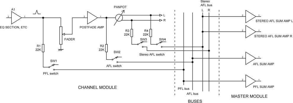
Figure 22.37 Comprehensive system with PFL and mono and stereo AFL.
A SIP system requires an electronically controlled mute on each channel. When the SIP button on a channel is pressed, every other channel is muted except that one. If two or more channels are solo-ed, they are left unmuted while the rest of the channels are muted.
The basic SIP system therefore has a SIP-detect bus, which works in just the same way as a PFL-detect bus. This determines when one or more SIP switches are pressed and activates a SIP mute bus that potentially mutes all the channels; however, if the SIP switch on a channel is pressed, it intercepts the mute signal and prevents it from operating on that channel. The basic scheme is shown in Figure 22.38.

SIP is a destructive solo, and you really, really don’t want to trigger it during a live performance. Therefore a “solo-safe” switch is usually fitted in the master section to act as a safety-catch or Molly-guard and prevent accidental operation. When it is engaged, the solo system usually acts as a PFL system instead, which is safe to use during performance.
Talkback Microphone Amplifiers
Most contemporary talkback systems have a small electret microphone mounted flush with the master module panel. The microphones used typically have an internal head amplifier that buffers the high impedance of the electret element, and all else that is needed is an amplifier stage with variable gain over a wide range. A typical arrangement is shown in Figure 22.39; gain is variable from 0 to +55 dB by RV1, with C4 keeping it to unity at DC. Note that the microphone is powered through the filter network R1 and C1.

Figure 22.39 A typical talkback microphone amplifier, with gain variable from 0 to +55 dB.
Figure 22.39 includes a couple of subtle but important design features. First, the second changeovers of the talkback routing switches are connected into the feedback network so that when none of them are pressed, the amplifier gain is reduced to unity. This prevents the microphone amplifier from clipping continuously if the gain is turned up but talkback is not in use; the resulting distorted waveforms would almost certainly crosstalk crunchily into other parts of the master module, such as the L-R mix summing amplifiers, and this would not be a good thing.
Second, you will have noticed that the value of C4 looks rather small compared with the low value of the gain endstop resistor R3 and in fact gives an LF roll-off that is -3 dB at 90 Hz. This is quite deliberate and is intended to control the amplitude of LF transients when the gain is set high.
Line-Up Oscillators
The oscillator output is not required to be a perfect sine wave; it only has to be good enough so that meter calibration is not affected. It also needs to look like a sine wave on an oscilloscope, or customer confidence will be undermined. Figure 22.40 shows a simple but dependable arrangement for a 1 kHz oscillator which does not require either expensive and fragile thermistors or complicated levelling circuitry.

Figure 22.40 1 kHz oscillator with diode amplitude stabilisation.
It consists of a feedback loop containing a band-pass filter and a soft clipping circuit. The waveform at the output of band-pass filter U1:A is amplified by U1:B and then soft-clipped by D1 and D2. This symmetrical clipping introduces odd-order harmonics only, which are more easily filtered out when the signal is fed back to the multiple-feedback band-pass filter U1:A. The distortion is approximately 0.5%. Note that when the oscillator is not in use, it is not routed to the buses but is also firmly stopped from oscillating at all by the closure of SW1. This is essential to remove any possibility of the oscillator crosstalking into the audio paths during normal operation. When SW1 is opened, this oscillator ramps up in amplitude in a very neat manner.
You will note the use of E24 resistor values to get the frequency as close to 1.0 kHz as possible and the parallel combination of R6 and R7 to give 745 Ω; this resistance is fairly critical for obtaining the minimum distortion, and the combination shown here gave dependably lower distortion than the E24 value of 750 Ω. The output level is dependent on the forward voltage of the two diodes, and so there is some variation with temperature, but it is insignificant in this application.
A somewhat more sophisticated 1 kHz oscillator is shown in Figure 22.41. This is based on the classic state-variable filter. A2 and A3 are integrators, while A1 performs the various subtractions and additions needed. R8 gives positive feedback to A1 of the band-pass output at A2, starting the oscillation. As its amplitude increases, the gain transistor Q1 turns on more, allowing more negative feedback through to counteract the positive feedback until a stable operating amplitude is reached. Diodes D1–D4 form a full-wave rectifier so that only one transistor is needed to handle both half-cycles. When SW1 is open, there is maximal negative feedback to A1 and the circuit does not oscillate, so there is no possibility of crosstalk. This function can be equally well performed by a JFET to ground, and it is common for sound-reinforcement consoles to have a SAFE switch that disables the oscillator and also the solo-in-place system so they cannot be accidentally used during a performance.
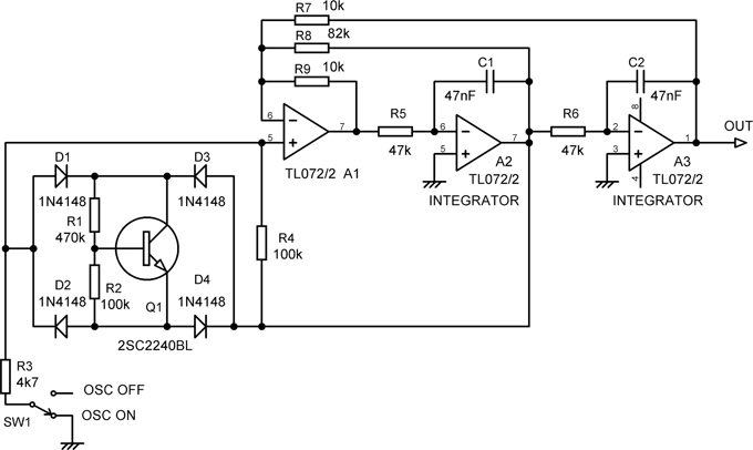
This oscillator is slightly more complicated than the previous version but has the advantage that it is more flexible in terms of setting the output voltage by adjusting R1 and R2 and also gives lower distortion due to the gentler amplitude control. An important point is that the output is taken from the second integrator, which in a state-variable filter gives a low-pass output, The extra filtering means that the distortion here is lower than at the band-pass output.
The next step up in oscillator sophistication is to provide two switched frequencies, usually 1 kHz and 10 kHz. The higher frequency was historically used for checking the azimuth adjustment of tape machine heads (when the azimuth of a tape head is maladjusted, the high-frequency response falls off badly). Nowadays, it is less useful but can still come in handy for quick frequency response checks. It is therefore very important that the output level is exactly the same for the two frequencies, and the oscillator shown in Figure 22.42 therefore has a more complex level-control loop.
The oscillator is based on the classic Wien bridge configuration, with the oscillation frequency controlled by R8, R9, C1 and R5, R6, C2. When running at 1 kHz R8, R9, and R5, R6 are in circuit. For 10 kHz, SW1 is pressed, and R5 and R9 are now shorted out, raising the operating frequency. The level control loop operation is as follows: when SW2 is pressed, the short circuit across R1 in the negative feedback loop R1, R2 which prevents oscillation is removed and the amplitude of oscillation ramps up. When it reaches the desired level, Zener diode D1 begins to conduct on positive peaks and turns on the common-base transistor Q1 (D1 also conducts on negative half-cycles, but Q1 does not respond and is protected from reverse bias by clamp D2). The collector current of Q1 charges C3 and Q2 turns on, pulling down the gate of JFET Q3 and increasing its channel resistance, thus increasing the amount of negative feedback through R1, R2 and regulating the level. Q3 is a J112 FET, a type that is optimised for voltage-controlled resistance (VCR) operation. The network R3, R4 not only acts as the collector load for Q2 but also feeds half the Vds of Q3 to its own gate; this is a classic method of reducing even-order distortion in JFETs and is dealt with in more detail in Chapter 24. C3 and R10 set the time-constant of the control loop, and their values have a strong effect on oscillator distortion. Q1 and Q2 can be any high-beta transistor types.
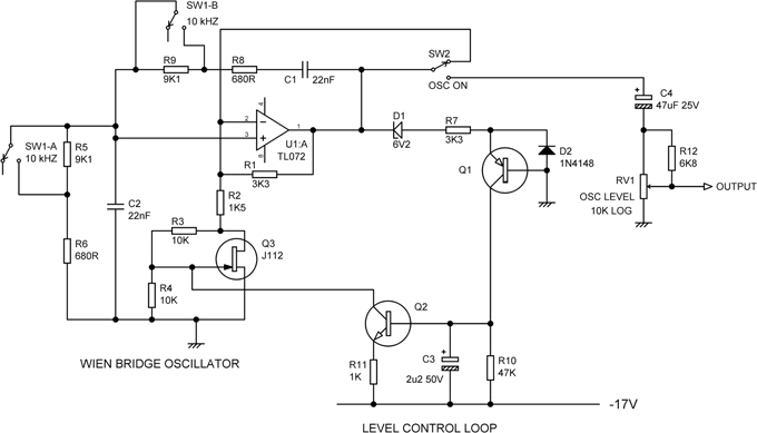
Figure 22.42 Switched 1 kHz/10 kHz oscillator with FET amplitude stabilisation.
Larger mixers often have more sophisticated oscillators with fully variable frequency and sometimes a choice of a square wave output. Oscillator design is a massive subject on its own, and there is no space to get deeper into it here.
The Flash Bus
On a console of any size, it can be hard to find a single PFL button that is down, and so taking over the monitor path, even if the PFL switches are illuminated. All too often, you might find yourself looking for a single indication in a sea of lit-up switches. Making the PFL LEDS a distinctive colour only helps a bit. I therefore persuaded Soundcraft that flashing the PFL LEDs at 2 Hz was a good idea. They would have to flash in synchrony, so the desk did not look like a demented Christmas tree, and thus having individual oscillators for each LED was out of the question; it would also have been prodigal of parts. This is of course trivial if all your LEDs are controlled by digital means, but in an era when most consoles had no housekeeping microcontroller or other on-board computer, it was more of a challenge. Since analogue-only consoles (some even with inductors in the EQ) are having a revival, this technology remains very relevant.
Clearly a common “flash signal” would have to be distributed to each mixer module. Simple enough, but most of the mixers for which this technology was intended had their bus connection made with IDC cable. This has a relatively high capacitance between conductors, and so sending a sharp-edged 5 V logic signal down it would have been a recipe for disaster. Be aware that grounding conductors in an IDC cable does not make them perfect screens; see the tests on PCB track-to-track crosstalk in Chapter 2. I therefore decided that the way to send the flash signal was as a 2 Hz sine wave. Experiment proved (and I don’t think it could have been determined in any other way) that a low-distortion sine wave was not required; 1% THD was low enough to ensure no detectable crosstalk into the audio buses. Of course, 2 Hz is well below audio and unlikely to capacitively couple into anything. Nonetheless, this is not the sort of thing to leave to chance.
The master oscillator was therefore a simple two-opamp circuit with amplitude stabilisation by silicon diodes; see Figure 22.43. The first stage around A1 is a multiple-feedback band-pass filter, and that around A2 is an inverting amplifier with diode limiting. This works just like the 1 kHz oscillator in Figure 22.40. It is important to use FET-input opamps (this is a good way to use up venerable TL072s), as the circuit impedances are high to keep the capacitors small. Electrolytics are used because the frequency is not critical, and neither is the distortion content of the output; care is taken that they are correctly biased.

Figure 22.43 2 Hz flash bus oscillator with diode amplitude stabilisation.
There is only one master flash oscillator, but there is one or more PFL LED in every module. Therefore, the LED control circuitry must be very simple to keep down both cost and the PCB area required. This is shown on the right of Figure 22.43. Resistors R10, R11, and Q1 are required to control the LED locally, and the only extra component in the channel module is one single resistor R9; it would be hard to make it more economical. Note that the sine wave amplitude is controlled so that reverse-bias precautions for the base of Q1 are not required. The output sine wave is centred around -17 V, as set by R3 and R4; since the emitter of Q1 sits on the -22 V rail (also used to power JFET switching; see Chapter 21), the flash bus oscillator must produce a signal just above this rail, which is achieved by the level-shift network D3, R8. The two amplifiers A1, A2 are powered from the 0 V and the -22 V rails.
When a channel PFL button is pressed, the voltage applied to R10 goes high and Q1 turns off, turning on the LED D4. The flash bus signal coming in through R9 overcomes that via R10 and periodically turns Q1 on, causing the LED to flash.
The flash bus technology was developed in 1983/84, and the first console to which it was applied was the TS24. It was still in use, virtually unchanged, in the Vienna-2 console, which was released in November 1994.
Power Supply Protection
A large mixing console typically consists of many modules, and a fault that means a power rail shorted to ground or worse can occur in any of them. A properly designed power supply will have full short-circuit protection and should survive this, but until you fix it, the whole console is out of action. You first have to locate the faulty module, and that will take time. At a live gig, it means disaster.
For this reason, modular consoles normally have some sort of fusing that limits the effect of a shorted rail to one module. A very popular choice in the heyday of the analogue console was not to use fuses as such but the much cheaper approach of putting 10 Ω resistors in series with each rail. Rather than use expensive fusible resistors, ordinary ¼ W types were used with their leads pre-formed to raise them above the PCB and so avoid it being damaged if ignition did occur.
In a complex module, the voltage drop across 10 Ω resistors becomes excessive, and there is also the question of how much signal voltage will exist on the inside of the resistor. Therefore, two or three sets of fuse resistors are used to split up the power demand between them.
Console Cooling and Component Lifetimes
Large mixing consoles have a lot of amount of electronics packed into a small space, both to reduce the size of the console so it is easier to install and to bring all the controls within a reasonable reach. This means that natural convection cooling is often barely adequate. It is made more difficult by the fact that open cooling vents on the top of a console are not popular due to the possibility of various beverages being poured into the works, with an excellent chance of catastrophic results. Elevated internal console temperatures are rarely high enough to cause semiconductor failures but have two bad consequences:
First, over time, the electrolytic capacitors will dry out and drop in value. This loss of capacitance can be dramatic; a 100 μF component can fall to 10 nF. This in turn causes two further bad consequences: the LF response of the console degrades as coupling capacitors drop in value, and opamps go unstable as rail decoupling capacitors become ineffective. In a large studio console, this can mean that its life is only 10 years before all the electrolytics need replacing. This “recapping” procedure is, as you might imagine, a lengthy and expensive process that can be done only by companies with specialised skills.
The average electrolytic capacitor has a temperature rating of 85°C. This does not mean that no capacitor degradation occurs below that temperature; degradation is happening all the time, but it accelerates rapidly as temperature rises, roughly doubling in speed with each 10°C increase. 85°C is the temperature at which capacitor life has dropped to a nominal 1000 hours, which is only 49 days, and so obviously they must be operated at a much lower temperature than that to get a reasonable equipment lifetime. Electrolytic capacitors rated at 105°C have recently fallen in price to the point at which they are a viable alternative, and at a given temperature, this increases lifetime by a factor of four. The best recapping facilities use low-ESR 105°C capacitors exclusively for replacements and, in strategic places, increase the value fitted so the life is longer before the value falls too low. This obviously requires an intimate knowledge of highly complex consoles and should only be undertaken by professionals such as GJC Designs. [1]
Second, if silver contacts are used in switches or relays, the rate at which they are corroded by atmospheric hydrogen sulphide, creating non-conducting silver sulphide and causing the contacts to fail, also increases rapidly with temperature. Once again it roughly doubles in speed with each 10°C increase.
The obvious way to improve console cooling is to add fans to increase the air flow. Fans are very undesirable in consoles installed in recording studios because of the acoustic noise they generate and are rarely if ever used. They are, however, sometimes fitted in PA consoles, though still with considerable care to minimise the noise they create. When this is done by running the fan at low speeds, at the low end of its specified voltage range, great caution is needed. After a period of use, the fan may stop altogether as the bearings become worn, and how long this takes is not readily predictable. Sleeve bearings seem to be worse than ball bearings for this. The use of fans is to a large extent a last resort, and every effort should be made to induce adequate cooling by convection alone.
Reference
[1] GJC Designs www.gjcdesigns.net/ Accessed Oct 2013