CHAPTER 24
Level Control and Special Circuits
Gain-Control Elements
A circuit block that gives voltage-control of gain is a difficult thing to implement. The basic function is simply that of multiplication, but most of the practical techniques introduce significant distortion. In every case, distortion and noise can be traded off by altering the operating level, but in some techniques, the non-linearity is so great that a compromise that meets modern performance standards is simply not possible.
A Brief History of Gain-Control Elements
The difficulty of implementing a good voltage-variable gain element is testified to by the number of technologies that have been tried. A variable attenuator could be made by varying the current flow through diodes, which varied their effective resistance; the control signal inevitably got mixed up with the audio signal, and linearity was poor. Optical combinations of filament bulbs and cadmium-sulphide photoresistors gave very good control-signal isolation, but operation was slow because of the thermal inertia of the filament. Later versions used LEDs and were much faster, but the non-linearity of the photoresistors remained a limitation. Chopper systems, which turned the signal hard on and off at an ultrasonic frequency, with a variable mark-space ratio, and then reconstructed the signal with a low-pass filter gave fast response and reasonable linearity. However, it was difficult to get a wide control range, and effectively removing all the switching frequencies required a fairly complicated filter. A long time ago, I designed just such a variable attenuator, using 4016 analogue gates for the switching and a clock frequency of 160 kHz. The gain was difficult to control below -40 dB, and it never made it to production, which on the whole was probably just as well.
JFETs
The introduction of JFETs (junction-FETs as opposed to MOSFETs) as gain control devices was a great advance. These devices promised good isolation between control-voltage and signal, instantaneous operation, and lower distortion than existing methods. These advantages do exist, but there are some less desirable features, such as a highly non-linear gain/CV law that varies significantly from specimen to specimen, as a result of process tolerances. Signal-CV isolation is absolute in the DC sense, the gate looking like a very-low-leakage reverse-biased diode, but there is always some gate-channel capacitance, which means that fast edges on the control voltage can get through to the signal path.
The use of JFETs for on/off signal control rather than voltage-controlled attenuation is covered in Chapter 21 on signal switching.
A JFET used as a voltage-controlled attenuator is operated below pinch-off, i.e. at low values of Vds that allow it to operate more like a resistor than a constant-current source. Some JFET types are better than others for this job, the 2N5457 and the 2N5459 being particularly favoured in the mid-seventies.

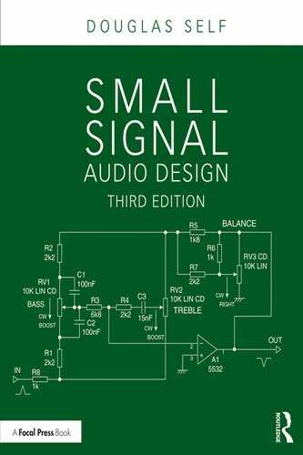
Figure 24.1 The basic voltage-controlled JFET attenuator circuit.
Figure 24.1 shows the most basic voltage-controlled JFET attenuator circuit. When N-channel FETs are used, as is normally the case, the control voltage must go negative of ground to turn off the JFET and give the minimum-attenuation condition. The maximum attenuation is limited by the Rds(on) of the JFET to about 45 dB for practical circuitry. The attenuation law is highly non-linear and variable between specimens of the same JFET; to some extent, this can be trimmed out by applying a constant DC bias to the control voltage, but minor variations in the shape of the control law still remain. One of the advantages of this circuit is that when there is no gain reduction, the JFET is biased hard off and there is no extra distortion introduced, though there will be Johnson noise from the series resistor. This makes JFETs useful in limiter applications where gain reduction occurs only briefly and intermittently; JFETs are much cheaper than VCAs.
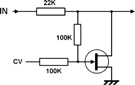
With the JFET conducting, the major non-linearity is second-harmonic distortion, which can be much reduced by adding half the drain-source voltage to the gate-control voltage, as in Figure 24.2. Note that it is half the drain-source voltage that is applied, not half of the input signal. The ratio is not critical – getting it right within 10% seems to give all the linearisation available. A serious problem with this circuit is the control-voltage feedthrough into the signal path. One answer is to add a DC-blocking capacitor C as in Figure 24.3; this stops DC but does nothing to stop fast transient feedthrough.
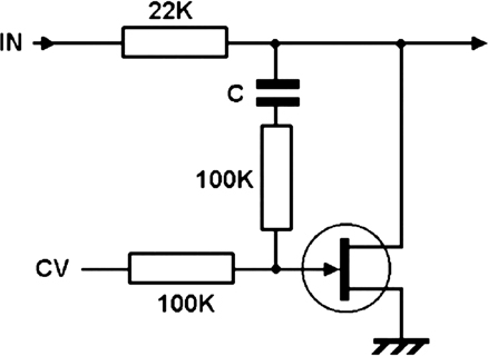
Another problem is that the presence of C adds an extra low-pass time-constant to the applied control voltage. In feedback limiters, this can cause instability of the control loop, typically causing the gain reduction to suddenly snap to the maximum value, followed by a slow decay back to normal operating conditions. This is not a good thing. Both problems can be solved by using a unity-gain buffer amplifier to isolate the JFET gate network from the signal path, as shown in Figure 24.4.
Because of their unhelpful control-laws, JFETs were most useful in feedback-type compressors and limiters, where the feedback loop linearised the law; more on that later. I produced a compressors/limiter design for Wireless World [1] when the application of FETs in this way was relatively new. It was published some years after I designed it. The linearity limitation remains, and JFETs are now rarely used in compressors and limiters (except for those which deliberately embrace obsolescent technologies), having been replaced by VCAs. They are, however, still useful in noise-gates, because as shown, they can be configured so that when the noise-gate is open, the JFET is firmly off and introduces no signal degradation at all. I repeat that a JFET is much cheaper than a VCA.

Operational Transconductance Amplifiers (OTAs)
An operational transconductance amplifier (OTA) gives a current output for a voltage difference input, and the amount of current you get for a given input voltage is determined by the current that is made to flow into a control port, giving a variable-gain capability. The output stage is a high-impedance current-source rather than the low-impedance voltage source of the conventional opamp, and the output current must be converted to a voltage, usually using a simple resistive load. Buffering is then needed to give a low-impedance output. Despite the name –operational transconductance amplifier –this device is not used like a conventional opamp when it is being used to give variable gain. There is no negative feedback around the device, as this would prevent the gain varying, and for acceptable linearity, the differential input voltages should be kept to 20 mV or less. Distortion is mostly third harmonic and comes from the input pair transistors.
The best known operational transconductance amplifier was the CA3080E, and a typical voltage-controlled gain circuit for it is shown in Figure 24.5. A1 is the OTA, R1 and R2 reduce the input level so it is suitable for the device input transistors, R3 is the I/V conversion resistor, and A2 is a conventional opamp acting as the output buffer. The THD is about 0.15% for a +5 dBu input level. Note the OTA symbol has a current source symbol attached to its output.
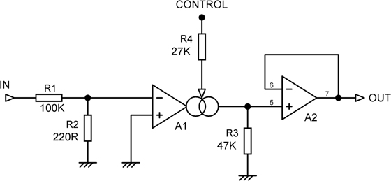
Figure 24.5 A typical gain-control circuit using the 3080E operational transconductance amplifier.
Another OTA, called the LM13600, was introduced later by National Semiconductor; this is a dual part and has distortion-compensation diodes in the input stage, which are claimed to have improved linearity fourfold. I have to say that I found that the difference in practical applications was not that large. It also has built-in Darlington output buffers. The LM13600 has now been replaced by the LM13700; the CA3080E went out of production in 2005. The LM13700 is used in much the same way as the CA3080E.
You are probably thinking by now that transconductance amplifiers belong in the history section of this chapter; they are placed here because their flexibility has kept them very popular with builders of analogue synthesisers.
Voltage-Controlled Amplifiers (VCAs)
Voltage-controlled amplifier (VCA) is the name given to a specific kind of variable-gain device. It is essentially a four-quadrant multiplier and is a current-in, current-out device, which therefore needs some support circuitry if it is to interface with the normal voltage-driven world.
Since the input port is a virtual earth, converting the input voltage into an input current requires only a resistor; see R1 in the basic circuit of Figure 24.6. Converting the output current into an output voltage is less easy and requires a shunt-feedback amplifier A1, as it is essential to avoid signal voltages on the output port. This is a transadmittance amplifier (current in, voltage out). An important advantage of this circuit is that it does not phase invert. It looks as if it does –the amplifier A1 certainly inverts –but so does the VCA internally, so the output remains in phase, which is of course essential for mixing console use.
Because of their log/antilog operation, VCAs are characterised by an exponential control characteristic, so gain varies directly in decibels with control voltage. This is extremely convenient, as it means that a linear fader can be used to control gain over a wide range; however, this is in practice less than ideal, as it spreads out the less important higher attenuation range too much. Special “VCA-law” faders are made that squeeze the high attenuation range so the normal operating range can be expanded.
The evolution of VCA technology starts in about 1970, based on the “Blackmer gain cell” developed by David Blackmer of dbx, Inc., and VCA history is a fascinating field in itself; see [2]. Another of the very early models was the Allison EGC-101, which gave improved linearity through Class-A operation. [3] The study of the internal operation of VCAs is also a big subject, and regrettably, I don’t have the space to go into the details here. An article in Studio Sound [4] gives a good deal of information on the internals. Other useful references on the technology are [5] and [6].
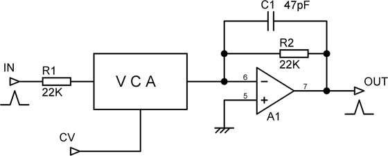
For many years, the “standard” VCA was the DBX2150, of which I have deployed more than I care to contemplate in VCA sub-group systems and console automation; more modern ones are represented by parts like the THAT 2181. A typical application circuit suitable for both is shown in Figure 24.7.
You will note that a symmetry trim pot is required; this is set to minimise second-harmonic generation. A THD analyser is required to make this adjustment, but on the positive side, once set, it stays set and need never be touched again unless the VCA is replaced. Modern VCAs are very good; the THD at 1 Vrms with 0 dB gain can be as low as 0.002%. The off-isolation (or offness, as I prefer to call it) can be as good as -110 dB at 1 kHz but will almost certainly be worse at higher frequencies as it depends on stray capacitance. This is why the SIP package is preferred; as shown in Figure 24.7, it keeps the input and output pins as far apart as possible. A crucial layout requirement is that the “hot” end of R1 is kept as far away as practicable from Pin 8 of the VCA, even if it means extending the track between R1 and VCA Pin 1. This track is at virtual earth and susceptible to capacitive crosstalk, so keep unrelated signals well away from it.
Figure 24.7 A typical gain-control circuit using the 2150 VCA. The eight-pin SIP package is almost always used for VCAs.
The control law (which is set by transistor physics and is therefore dependable) is 6 mV/dB at the actual VCA control pin, and this is inconveniently low. A scaling amplifier A2 is therefore used so the control voltage has a more useful range, such as 0 to 10 V. The presence of this amplifier also gives the opportunity for control voltage filtering and changes of ground reference. The voltage applied to the control port must be at low impedance (basically an opamp output is the only source that will do) and absolutely free from contamination by any sort of signal or avoidable noise. Contamination with even a trace of the signal being controlled will cause excess distortion.
The capacitor C1 shown across the I-V conversion opamp feedback resistor is always required for HF stability due to the destabilising capacitance seen looking into the VCA output port.
In other places in this book, I have described how noise can be reduced by using multiple transistors or multiple opamps in parallel. This also works with VCAs; you simply put N of them in parallel and connect their outputs to a single shunt-feedback amplifier with a suitably reduced feedback resistor, as shown in Figure 24.8. Two VCAs give a 3 dB improvement and four a 6 dB benefit. There are of course limits as to how far you can go with this sort of thing; high-quality VCAs are relatively expensive. Four in parallel have been used in high-quality compressor/limiters such as the Connor. Eight VCAs are employed by That Corporation in their 202 module, which is used in high-end consoles such as those by SSL.
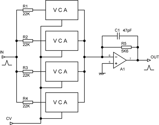
Figure 24.8 Using multiple VCAs in parallel to reduce noise. Each doubling of numbers theoretically reduces noise by 3 dB.
Compressors and Limiters
Compressors and limiters are devices that control the dynamic range of a signal. The device acts like a rapid volume control that reduces the gain when the signal level becomes excessive.
A compressor reduces the general dynamic range of a signal for the majority of the time. A typical application is control of microphone levels when the talent does not make microphone technique their top priority. This means that it is applying some amount of gain reduction most of the time, so the gain-control element is active, and it is important that it is relatively distortion free and without other audible defects.
A limiter, in contrast, has as its main function the prevention of overload and horribly audible clipping. When loudspeakers and AM transmitters are being driven, it may actually prevent expensive equipment damage. Transmitters require the extra protection of a clipper circuit; see the separate section on these. Since a limiter operates relatively rarely (assuming the system is being operated correctly), it is less important that the gain-control element is distortion free.
Figure 24.9 shows the relationships between input and output levels for compression and limiting. The compressor law begins gain reduction at a lower threshold level and has a moderate slope thereafter; the slope shown here is 3:1, which is typical. The limiter law has a higher threshold and only acts when overload is imminent; the slope is much flatter so that even very high signal levels cannot reach the overload point; the slope here is 10:1.
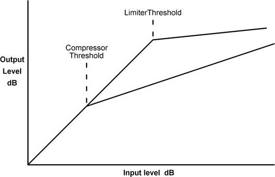
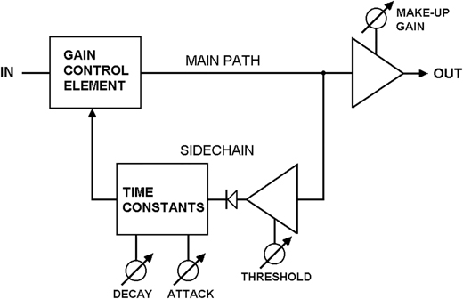
Figure 24.10 Block diagram of a feedback compressor/limiter.
Compressors and limiters do a similar job, using much the same hardware with different parameter settings, so the functions are often combined in a compressor/limiter. Figure 24.10 gives the block diagram of a feedback compressor/limiter. The output signal is amplified and, if it exceeds a certain threshold, applied to a rectifier with a fast-attack slow-decay characteristic. This part of the system is called the sidechain, to emphasise that the signal does not pass through it. The resulting control voltage is applied to the gain-control element, and as the signal level increases the gain is reduced, reducing the variations in output level. The sidechain may use either peak or RMS sensing; the latter is considered by some to relate better to our perception of loudness and give a less obtrusive effect.
The laws shown in Figure 24.9 have “hard knees” as the gain laws change abruptly at the threshold. A “soft knee” slowly increases the compression ratio as the level increases, giving a curve that gradually attains the desired compression ratio. A “soft knee” is considered to make the change from uncompressed to compressed less audible, especially for higher compression ratios.
If the threshold is set low and the sidechain gain is also low, the system works as a compressor, the gain reduction acting to reduce the general dynamic range of the output signal, hopefully without obvious side effects. If the threshold is set high and the sidechain gain is also high, we have instead a limiter. The signal will be untouched until it exceeds the threshold, and then gain reduction is applied strongly to prevent the output level significantly increasing.
Compressor/limiters can work in either feedforward or feedback modes, each of which has its own advantages and problems. In the feedback mode, the compression law tends to be inherently linear because of the feedback around the level-control loop. The feedback configuration has the advantage that the output level set does not depend on the control-voltage law of the gain element.
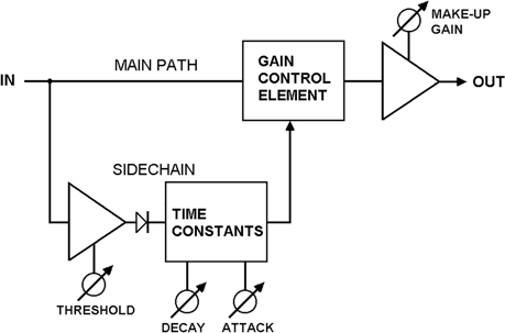
Figure 24.11 Block diagram of a feedforward compressor/limiter.
With feedforward, as in Figure 24.11, the compression law depends on the control-voltage law of the gain element. If this is a VCA with a very predictable law, no problem. However, other gain elements such as FETs sometimes have their uses –with FETs, the advantage is that there is no signal degradation when there is no gain reduction. There is, however, also a highly non-linear control-voltage law to deal with, and it is not practical to bend this into a more desirable log law.
The way to solve this is shown in Figure 24.12, which assumes that two matched gain elements are easier to make than one with the required law. The sidechain path contains a feedback limiter, and the control voltage this generates is fed to the second gain element, which acts in feedforward mode. Typically the gain elements are matched as well as possible by trimming.
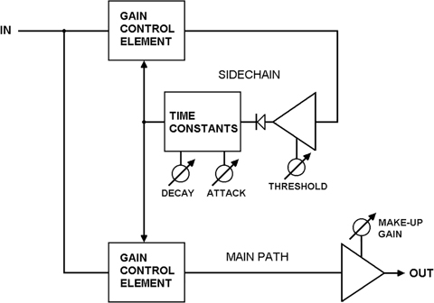
Figure 24.12 A combined feedforward/feedback compressor/limiter.
So far we have assumed that the sidechain dynamics consist only of two simple time-constants for attack and decay. In many cases, this will give rise to objectionable effects, and more sophisticated control measures have been developed to deal with the problems. Even if a gain-control element is completely linear when the control voltage is fixed, rapid CV changes put distortion into the waveform.
Attack Artefacts
When a fast attack is used to control level (typically when the unit is being used as a limiter) and prevent overshoot, it tends to bite chunks out of the controlled waveform, as a natural consequence of a rapid drop in gain. Isolated cases of this usually pass unnoticed, but repeated occurrences are perceived as a crackling noise. This can be controlled by the use of dual attack times, with the faster time switched in if the signal peak exceeds criteria for amplitude and rate of rise, but the only complete solution to this problem is a delay-line compressor/limiter, as seen in Figure 24.13.
A delay in the signal path between the sidechain takeoff point and the gain element allows a feedforward sidechain to react relatively slowly and still have the gain reduced before the signal peak reaches the gain-control element. (This is not possible with the feedback compressor/limiter configuration because the sidechain feed is taken after the gain-control element and therefore after the delay.) The difficulty is that the signal is delayed at all times; this will cause problems if it is being mixed with undelayed signals, and furthermore, the delay section has to be of high quality as it passes the main signal, not just the sidechain information. A well-known BBC design of circa 1967 used a strictly analogue 320 μsec delay-line made up of 10 LCR second-order all-pass filter sections. [7] This worked very well but is obviously an expensive technique. An active filter delay-line would be cheaper but still involves a significant amount of circuitry and a number of close-tolerance components. Nowadays, a high-quality digital delay using 24-bit converters can be constructed relatively easily.

Figure 24.13 Block diagram of a feedforward compressor/limiter with delay.
Decay Artefacts
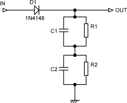
Since the sidechain contains either a peak or RMS detecting rectifier, the timing capacitor will have on it a ripple waveform resulting from cyclical charge and discharge, exactly as in a power-supply reservoir capacitor. This waveform modulates the signal path gain and generates distortion; the effect can be severe. In most compressor/limiter usage, the attack time has to be fast, but often the decay time can be made much longer, reducing the amplitude of the ripple and reducing distortion. However, in some applications, the decay has to be short for rapid recovery from brief level excursions, or the general level of the signal will be unduly depressed. An effective and widely adopted solution to this problem is the use of dual time-constants. See Figure 24.14 for a simple implementation, where the short time-constant R1, C1 responds to short-term level changes while the long time-constant R2, C2 copes with the general trend.
Another elaboration is a hold circuit which prevents the decay from beginning if any attack events have occurred in, say, the preceding 20 msec. This helps to prevent sudden and obvious gain changes, often called by the highly descriptive term “pumping”. If the noise background is significant, as with many live news recordings, then even slow gain changes produce a distracting effect called “breathing” because that’s just what it sounds like.
Subtractive VCA Control
While modern VCAs are very good, they still introduce more noise and distortion than a typical well-designed chain of 5532 opamps, and as mentioned, FETs are therefore still favoured for some compressor/limiter applications, as they introduce no degradation when not bringing about gain reduction. However, the predictable characteristics of VCAs are very attractive, and it would be nice to combine the advantages of both.
This can be done; whether I invented the technique first I have no idea, but it was all a long time ago. The concept, as shown in Figure 24.15, is not to send the signal through a VCA with 0 dB gain when no gain reduction is required but to have the VCA normally hard off and then turning it on to reduce the gain. When the VCA is off, the circuit acts as a simple unity-gain inverting amplifier, and there is minimal signal degradation.
Note that point about inverting –this circuit phase inverts although the standard VCA circuit does not. As the VCA gain is turned up, it lets more signal current through to the summing point of A1, and since this is out of phase due to the internal inversion of the VCA, there is partial cancellation, and the overall gain falls. When the VCA is set to 0 dB gain, theoretically there is complete cancellation and the overall circuit is off. In practice, the tolerances in R1, R3 and in the VCA set a limit to the practicable minimum gain, but the range is more than enough for effective dynamics control.
You may have spotted the potential snag. If the gain of the VCA goes above 0 dB (which corresponds with a control voltage of 0 V), the overall gain will begin to rise again. With a feedback-type compressor/limiter this, could be disastrous, as the sidechain will try to reduce the gain, but it will simply increase it further, and the system will latch up solid. This can be prevented by the simple expedient of using an active clamp circuit to prevent the control voltage rising even a millivolt above 0 V. Note that because of the subtractive action, the gain law is no longer linear in dBs, and so this plan is better suited to feedback compressor/limiters. I put this system into a broadcast console in 1990, and it worked very well.
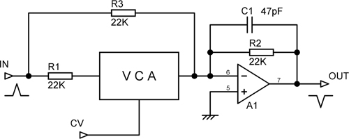
Figure 24.15 A VCA gain control arranged so that no signal passes through it when no gain reduction is occurring.
Noise Gates
A noise gate allows a signal through only when it is above a set threshold: the gate is said to be open or on. When the signal level drops below the threshold, the signal is either attenuated or stopped altogether, and the gate is closed or off. For effective noise reduction, the level of the signal must be above that of the noise; the threshold is set above the noise level so when there is no signal, the gate closes. Noise gates are not actually often used to discriminate against noise as such; in recording, they are more likely to be used to, for example, increase the isolation between the signals coming from a multi-mic’d drum kit. They are also used to provide the well-known “gated reverb” effect in which decaying reverb is cut off suddenly by a noise gate.
A noise gate is a rather different animal from a compressor/limiter. Its operation is much more on/off, and long time-constants are not normally used. This means that the non-linearity of an FET during intermediate degrees of gain reduction can be tolerated. In the traditional form of FET noise gate, as shown in Figure 24.16 and based on a design I did some years ago, FET distortion is reduced by attenuating the signal considerably –in this case by 32 dB –before applying it to the FET stage. This is done by R1, R4, and the signal is at a low impedance afterwards to keep noise down. The FET (actually two FETs here, to reduce Rds(on) and give a greater gain change) is at the bottom of the NFB network of a low-noise hybrid amplifier stage that restores the signal to its original level when the FET is on. When the FET is off, the gain is reduced to unity. This would only give an offness of -32 dB, which is not enough, so the network R9, PR1, R8 is added, which lets a little signal through to what is effectively an inverting input to the amplifier stage; when PR1 is correctly adjusted, there is effective cancellation, and the offness can easily exceed -80 dB. FET distortion is further reduced by adding half the drain-source voltage to the gate control voltage via buffer A3, as described earlier.
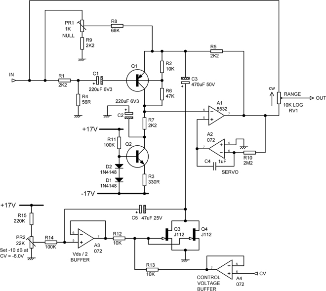
The low-noise amplifier is a hybrid stage, combining the low noise of the discrete input transistor Q1 with the open-loop gain and linearity of opamp A1. R2, R6 set up the DC conditions for Q1, while servo integrator A2 defines the DC operating point of A1, keeping its output at 0 V on average. Q2 is a current source that helps keep rail noise out of the collector circuit of Q1. The alert reader will spot the similarity between this stage and the moving-coil preamplifier stage in Chapter 10. The noise from the amplifier with the gate off is -106 dBu.
Many noise gates have a “range control” that allows the offness to be reduced if a more subtle effect is required. This is RV1 in Figure 24.16, an ordinary log pot that has the bottom of its track, which would normally be grounded, connected instead to the noise gate output. Offness is reduced by advancing the control so that some of the signal gets through even when the gate is off.
The sidechain of a noise gate is similar to that of a compressor/limiter, but there is a greater emphasis on fast attack times of 50 μsec or less, and special circuitry is used to charge the timing capacitor as quickly as possible.
Noise gates can also be made with VCAs, and this is the more usual method when a “dynamics section”, which can act as either a noise gate or a compressor/limiter, is squeezed into a mixer channel.
Clipping
Since clipping and its attendant distortion are things we normally strive to avoid, it may be thought perverse to study ways in which to induce it. Clipping circuits do have their uses, however. One application is in the protection of AM transmitters, where even momentary excursions beyond 100% modulation are unacceptable, because they lead to legal problems (sideband splatter causes the regulator to close you down) and technical problems (the transmitter blows up). Either way, you’re off the air. Limiters are the first line of defence, but they are liable to overshoot and maladjustment. A fixed-level clipping circuit, however, can absolutely prevent any signal exceeding its threshold. Clipping circuitry also has specialised uses in power amplifier design, where it can emulate the performance of a much more complex and expensive regulated power supply [8], or increase the flexibility of bridged amplifiers. [9]
To set down some of the requirements for the perfect clipping circuit:
- Clipping must be at well-defined symmetrical levels, constant with frequency and not dependent upon signal history.
- The top of the clipped waveform should be absolutely flat to give tight level control.
- The clipping level must be arbitrarily settable, without steps.
- There must be absolutely no degradation of the signal below the clipping threshold –or at any rate, no more than would be caused by going through an ordinary single opamp stage.
This last requirement is actually much more demanding than it appears, but it is essential. Let us examine the problem. I appreciate that clean audio clipping may be a bit of a minority interest, but it will be highly instructive to see just what difficulties arise and how they can be overcome.
Diode Clipping
If you look up “clipping circuits” in the average textbook, you will probably find something like Figure 24.17, where back-to-back diodes conduct when the signal exceeds their conduction threshold.
This fails to meet our requirements in several ways. First, the gradual onset of conduction in the diodes means that the clipping is soft, infringing requirements 2 and 4. And finally, it breaks 3 as well, because the clipping level can only be altered by changing the number of diode pairs used, giving 0.6 V steps.
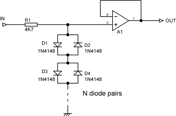
Figure 24.17 A simplest passive clipping circuit using diodes.
Figure 24.18 shows the force of this, the result of using various numbers of pairs of 1N4148 silicon signal diodes. The lower line descending from left to right is the noise floor, getting relatively lower as the input level increases. With one pair of diodes, distortion is already clearly above the noise floor for an input as low as 100 mVrms. The gradual increase in distortion after this as level increases shows that the clipping is distinctly soft and so introduces unacceptable distortion long before it effectively controls the level. An obvious extra snag is that a passive circuit like this has a significant output impedance; in most applications, some sort of output buffering like A1 will be required.
The very gradual onset of clipping shown above is due to the slow way in which the exponential conduction law of diodes begins. The clipping action can be made much sharper by connecting each diode to a suitable bias voltage so that it is firmly reverse-biased at low signal levels and only conducts when the signal is significantly above the bias voltage. The bias chain must have a low impedance to give a steep clipping characteristic, and so diodes are also used to establish the voltages. it would of course be possible to generate near-zero impedance supplies by using opamps to buffer resistive dividers (which also allow complete flexibility in setting the clipping threshold). However, if opamps are to be employed, there are better ways to use them, as we shall see later in this chapter.

Figure 24.18 Distortion against input level for one to six pairs of clipping diodes. The uneven spacing of the curves as diode pairs are added is due to the logarithmic X-axis for input level.


Figure 24.20 Distortion against input level for one or two pairs of diodes in the biasing chain.
A biased clipping circuit is shown in Figure 24.19, and the resulting distortion performance in Figure 24.20, for both one and two pairs of diodes in the biasing chain. The much steeper rise in distortion shows that the onset of clipping is much sharper; compare Trace 6 in Figure 24.18 with Trace 1 in Figure 24.20.
The clipping action of simple circuits like this is, however, still some way short of perfect, in that the clipped part of the waveform is not a dead flat horizontal line. Diodes do not suddenly become short circuits when they start to conduct, and the clipped part of the waveform bulges upwards somewhat. Clearly we need active circuitry to sharpen up the diode action.
Active Clipping With Transistors
The next step up in sophistication from simple diodes is the use of transistors for clipping. This is an active process in that the voltage applied to the base turns on the collector current. It is not simply a matter of using the base-collector or base-emitter diodes to replace the simple diodes in the previous section.
Figure 24.21a shows a basic transistor clipper with NPN and PNP devices shunting the signal path, and Figure 24.22 shows the distortion performance. A buffer is required for a low-impedance output; trace A in Figure 24.22 shows the result without an output buffer, and trace B shows the result with it. In the latter case, not only has the noise floor dropped due to less pickup on what is now a low-impedance output, but the distortion at a given level has risen significantly, as the low-pass action of a capacitive screened cable driven from a medium impedance has been eliminated.
In Figure 24.21b, the circuit is arranged so that extra drive is applied to the transistor bases via R2 because of the voltage drop across R1. This pulls down the clipped part of waveform in the centre and, with a correct choice of values, gives improved flatness. The circuit is based on a concept by Stefely. The distortion plot in Figure 24.23 is not very different.
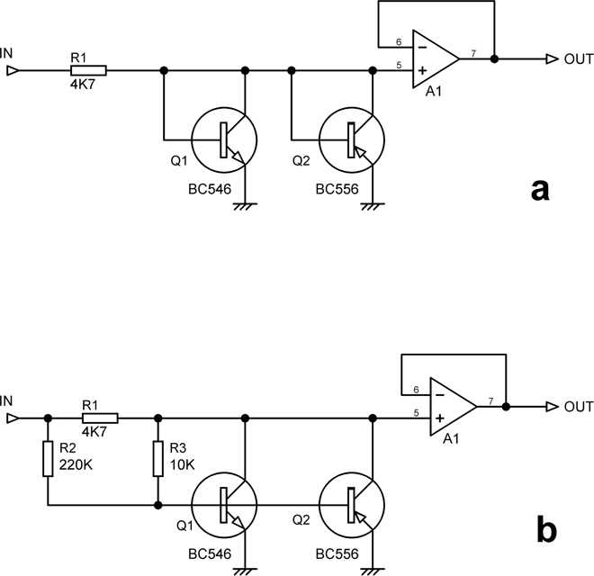
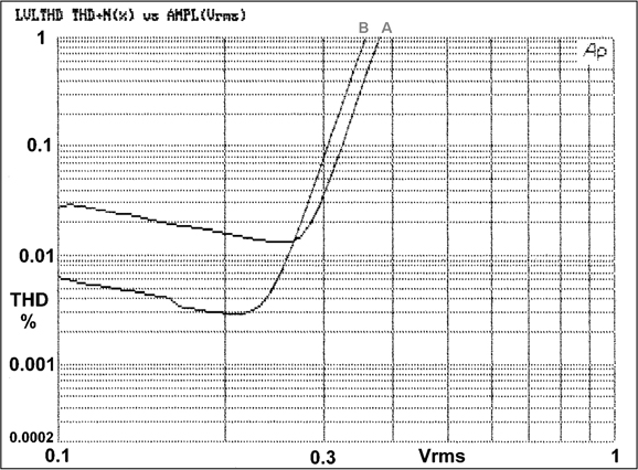
Figure 24.22 Distortion against input level for transistor clipper.
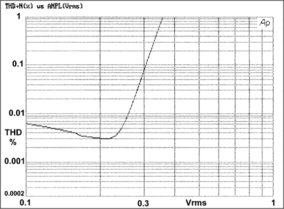
Figure 24.23 Distortion against input level for enhanced transistor clipper.
Active Clipping With Opamps
Opamps are noted for their versatility. However, using them to do precision clipping, with low distortion below the clipping point, is more difficult than it at first appears. Here I examine three ways of doing it, as the limitations of the first two approaches are highly instructive.
1. Clipping by Clamping
The first attempt is the direct descendant of the diode clipping circuits examined earlier and uses two active clamps A1, A3 to constrain the voltage at point A, downstream of the 4k7 resistor, as shown in Figure 24.24. Normally this point is between the two clipping thresholds, so the inverting input of A1 is positive of Vt-, and the opamp output is saturated negatively. D1 is therefore firmly reverse biased, and A1 has no effect on the voltage at A. Likewise, normally the inverting input of A2 is negative of Vt+, and D2 is held off.
When the voltage at X tries to exceed Vt+, the output of A2 swings negative and D2 pulls down point A to prevent it. The diode imperfections are servoed out by the open-loop gain of A2, so the clipping threshold is exactly Vt+, neglecting opamp offsets and other minor errors. In the same way, if point X tries to go below Vt-, the output of A1 swings positive and D1 conducts to clamp the output at this voltage. Like the passive diode clipper, this circuit has a significant output impedance (4k7 in normal operation), and so buffer A2 is added to give a low output impedance.
The two clipping thresholds can be set to any desired voltage, as they are derived from resistive dividers. They can of course be different, though an application in which this might be useful is not that easy to visualise.
The clamping-clipper circuit gives very clean clipping but falls down badly on the distortion it adds to signals below the clipping threshold of 2.2 Vrms. Figure 24.25 shows that distortion reaches an unacceptable 0.035% at 10 kHz and 2 Vrms; the 2 V trace is lower at LF because the relative noise floor is lower. This distortion occurs because point X is at a significant impedance and is connected to two opamps with JFET inputs, typically TL072s. These have non-linear capacitances to the IC substrate and cause distortion that worsens with frequency and level, as shown in Figures 24.25 and 24.26. See Chapter 4 for more details of this distortion mechanism. This effect could be eliminated by using opamps with bipolar inputs, but then the bias currents have to be dealt with. One advantage of this circuit is that it does not phase invert, unlike most active clipper circuits.
Figure 24.25 Distortion against frequency for the active-clamp clipping circuit.
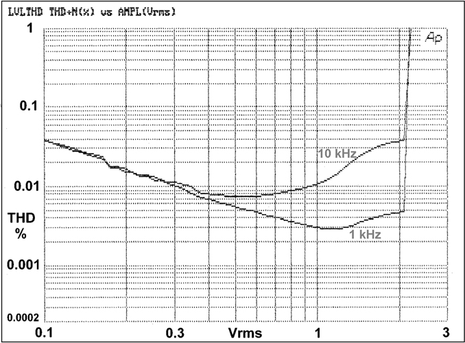
Figure 24.26 Distortion against input level for the active-clamp clipping circuit.
Figure 24.26 shows that at 10 kHz, distortion is beginning to appear when the input exceeds 300 mVrms, and it rises slowly until clipping begins just above 2 Vrms.
2. Negative-Feedback Clipping
Having found that clipping in the forward path has significant problems, we move to a configuration in which this takes place in the negative-feedback loop so the clipped output can be taken from an opamp output at low impedance. This also makes interfacing with the next stage simpler.
The circuit in Figure 24.27 works as follows: with no input, point X sits at +5 V and point Y sits at -5 V. When the output heads positive, eventually Y is pulled positive of the 0 V at the A1 inverting input, and D2 starts to conduct, reducing gain and giving clipping. Similarly, on sufficiently large negative output excursions, D1 will conduct. The clipping characteristic is rather soft; the gain cannot be reduced entirely to zero above the threshold because of the diode forward impedance in series with the source resistance of the 2k2–1 kΩ bias network. The latter can be reduced by using lower resistance values, but this loads the opamp output excessively and draws more power from the supply rails.

Figure 24.27 A negative-feedback clipper; the clipping threshold is set by the voltages at X and Y.
This configuration gives less sub-threshold distortion than the previous circuit by a factor of roughly three at 10 kHz, but it is still a long way from our requirement for “absolutely no degradation of the signal”, which some of you are by now probably thinking was a bit ambitious.
The distortion for a 3 Vrms input, which is well below the clipping threshold for this circuit, is shown by curve A in Figure 24.28, and it is instructive to wheel out the scientific method to find out what is going wrong with the linearity. The previous clamping-clipper circuit ran into trouble by driving non-linear opamp inputs from a non-zero impedance; that cannot be happening here, as both opamp inputs are at zero voltage, the inverting input so because there is always a healthy amount of shunt feedback.
So what might be the problem? We know that opamps have their linearity degraded by excessive output loading, and the two diode bias networks, being connected to rails that are effectively at AC ground, represent a significant load of (2k2 + 1 kΩ) in parallel with (2k2 + 1 kΩ), which works out to a total load of 1.6 kΩ on the output. This is quite enough to degrade the linearity of most opamps (see Chapter 4), but the idea is still only a hypothesis and needs testing.
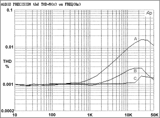
Figure 24.28 The distortion performance of the negative-feedback clipper against frequency for a 3 Vrms input. Plot A: basic distortion of Figure 24.27. Plot B: loading distortion eliminated by buffering A1 output. Plot C: with the diode chain disconnected.
This can be done experimentally by means of the circuit in Figure 24.29, which uses a separate voltage-follower A2 to drive the two bias networks, the clean output being taken off before it. Our hypothesis looks good, as eliminating the loading on A1 has much reduced the distortion, giving Plot B in Figure 24.28. This, however, still falls somewhat short of perfect linearity.
The distortion remaining in Plot B is due to negative feedback through the non-linear diode capacitances while they are still reverse-biased, i.e. below the clipping threshold. This can be demonstrated by disconnecting the output of A2 so clipping is disabled and points X and Y do not move. The diodes are still connected to the summing point at the inverting input of A1, which also does not move, and we now get Plot C in Figure 24.28, which is essentially the test gear distortion plus a little circuit noise.
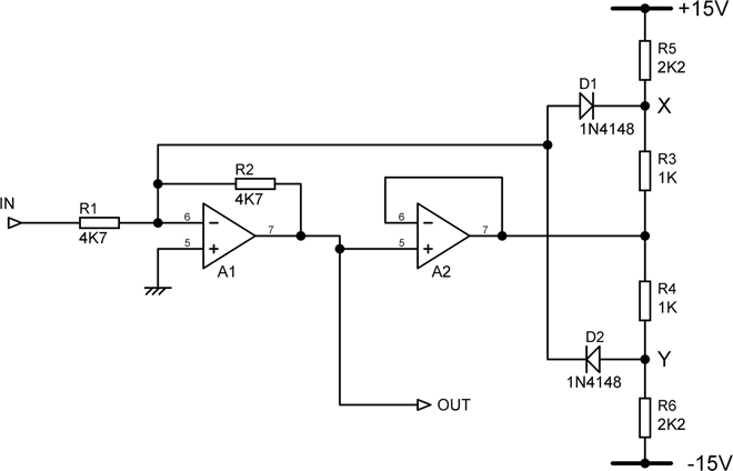
Figure 24.29 A modification of Figure 24.8 that removes the loading distortion from the signal path.
Putting extra opamps in a negative feedback loop is not something to be entered into lightly or inadvisedly because of the danger that accumulating phase shifts can make the loop unstable. However, it often works if the extra opamp is configured as a voltage-follower because the 100% local feedback in the follower makes its bandwidth as great as possible and significantly greater than that of an inverting stage, which works at a noise-gain of 2. Here it works dependably.
While this circuit is some way short of perfection, it can be useful sometimes, especially if there happens to be a spare opamp half left over to act as the buffer A2 in Figure 24.29. Don’t forget that this circuit gives a phase inversion.
3. Feedforward Clipping
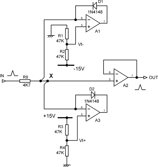
The Attempt 2 clipper demonstrated one way to reduce sub-threshold distortion, but it also highlighted the difficulty of getting hard clipping and tight level control by using negative-feedback techniques. While feedback is a most powerful technique, it is not the only way; sometimes feedforward does it better.
The circuit of a feedforward clipper is shown in Figure 24.30. Below the clipping level, it acts simply as a unity-gain inverting stage, with the forward path through R1. This configuration eliminates common-mode distortion in A2 during normal operation.
The clipping circuit consists of two shunt-feedback precision rectifiers A1, A3 that are biased by currents injected into their summing points via R2, R3, so they conduct only above the desired clipping threshold. A1 handles negative clipping; R2 injects 15 V/47 kΩ = 319 μA into the summing node of A1, and as long as this exceeds the current being pulled out of this node via R5 during negative inputs, it will be counteracted by feedback through D2. When the current through R5 exceeds that injected by R2, the opamp output must go positive, so it can maintain its inverting input at ground by feedback through D1 and R6. As before, the gain of the opamp A1 is used to “servo-out” the non-linearity of the diodes D1, D2.
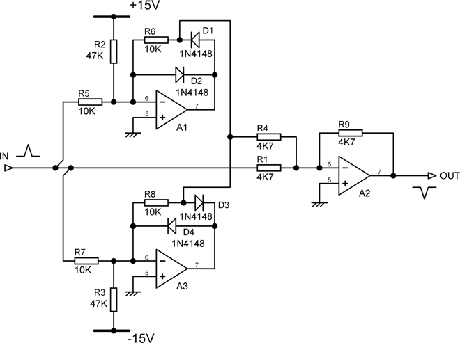
When D1 conducts, a clamped version of the input signal appears at the junction of R6 and D1, and a unity-gain but phase-inverted path is established through R4; the overall gain suddenly drops to zero as the two signals are cancelled at the summing point of A3, so the output cannot move any further and is clipped. The precision rectifier A3 acts in the same way for positive inputs.
Since A1 and A3 are never active at the same time, they can share the resistor R4, which makes for a very elegant circuit. The downside of this economy is that the active precision rectifier has to also drive the feedback resistance (R6 or R8) of the inactive precision rectifier, its other end being connected to virtual ground, and this will use up slightly more power. From this point of view, the saving of a resistor is not quite as elegant as it looks; if power economy is paramount, then separate cancellation resistors to each precision rectifier remove the problem.
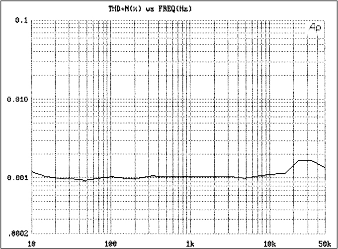
Figure 24.31 Distortion against frequency just below the clipping threshold. Input level 2 Vrms. This is once again the distortion of the test gear plus a little added noise.
As Figure 24.31 demonstrates, this circuit is a success. There is now no measurable distortion, even just below the clipping threshold. (The step around 20 kHz is an artefact of the test gear used.) The reason for this is that there are no opamp loading issues and no reverse-biased diodes with a distorted signal on one side connected to the audio path on the other side. The two clamp stages have zero output until the threshold is reached, with R4 being connected only to a virtual ground.
With perfectly accurate resistors, and indeed perfect opamps, this circuit would give complete cancellation, and the top of the clipped waveform would be absolutely flat. Cancellation processes have something of a dubious reputation in engineering circles because of the need for accurate matching of amplitude and phase to get a good cancellation. Where this depends on several factors –and particularly if semiconductor characteristics enter the equation –it can indeed be difficult to control. However, in this particular case, the cancellation accuracy depends only on a few well-matched resistors. 1% tolerance is quite good enough, and most modern resistors are this accurate. The only consequence of mismatching is a very slight curvature of the clipped part of the waveform, and this is not normally enough to be troublesome.
As shown by the phase spikes in the diagram, this circuit gives a phase inversion, and this must be taken into account during the system design.
Noise Generators
As with the introduction of deliberate clipping, it may seem perverse to go to a lot of trouble to generate noise when we have spent great efforts so far to minimise it. However, noise sources have their uses –for example, in loudspeaker testing, room equalisation, and in analogue synthesisers. Noise comes, as is well known, in various colours. This is not due to synaesthaesia (“Tuesdays are red!”) but to a convenient way of describing the spectral content of various particularly useful kinds of noise; see Chapter 1.
White noise has equal power in equal bandwidth, so there is the same power between 100 and 200 Hz as there is between 1100 and 1200 Hz. It is the type of noise produced by most electronic noise mechanisms.
Pink noise has equal power in equal ratios of bandwidth, so there is the same power between 100 and 200 Hz as there is between 200 and 400 Hz. The energy per Hz falls at 3 dB per octave as frequency increases. Pink noise is very important, as it gives a flat response when viewed on a third-octave or other constant percentage bandwidth spectrum analyser.
Red noise has its energy per Hz falling at 6 dB per octave; its main use is in synthesisers. There is more on noise of different colours in Chapter 1.
Most noise generators these days are digital, using calculations to produce pseudo-random white noise that is tightly defined in amplitude and spectral content. There are several ways to generate pseudo-random noise, of which the most common is the use of maximal-length sequences. These sequences repeat eventually and need to be rather longer than you might think to avoid any audible patterns in the noise; 10 seconds is a good starting value. There are other ways to produce pseudo-random noise, such as Kasami codes, but that is rather outside the province of this analogue book, so instead we will take a quick look at analogue noise generation.
The most popular method is to use the white noise produced when a bipolar transistor is reverse biased and works as a Zener diode, as shown in Figure 24.32. The collector is not connected to anything. This does the transistor no harm so long as the current through it is limited and is surprisingly consistent, when you consider that this is not exactly the official way to use a transistor. I took a collection of 10 BC184C transistors of varying pedigree and provenance and found that with an emitter current of 36 μA, the noise output varied between -61.5 dBu and -65.6 dBu, with one outlier at -56.9 dBu (bandwidth 22–22 kHz). The Zener voltage on the emitter was between 7.7 V and 8.9 V. When I tried a real Zener diode, of 6 V2 voltage, the noise output was much less, around -85 dBu. This is presumably because Zeners are designed to produce minimal noise, though they still generate much more than simple silicon diodes; noise is distinctly unwanted in voltage reference applications.
The transistor noise output is well below a millivolt, and a good deal of amplification is needed to get it up to a useful level. Figure 24.32 shows a humble TL072 performing this service; there is of course absolutely no point in using a low-noise opamp such as the 5532, and the low bias currents of the TL072 mean that high-value resistors can be used without DC offset troubles. Each stage has a gain of 27 dB. A point to remember is that the TL072 has limited open-loop bandwidth compared with more modern opamps, and if you try to take too much gain in one stage, this will lead to a high-frequency roll-off. The last amplifier stage must not be allowed to clip, as this will modify the energy spectrum. The output here is about 400 mVrms, so clipping will statistically be very rare. Bear in mind there was a 4 dB variation in noise output for different transistor samples, and a preset gain trim may be needed for some applications.

Figure 24.32 A white noise generator using a bipolar transistor as a Zener diode.
Pinkening Filters
Converting white noise into the much more useful pink noise is proverbially difficult because you can’t make a filter with a true -3 dB/octave slope, as filter slopes come in multiples of 6 dB/octave only. The only solution when you need a pinkening filter is a series of overlapping low-pass and high-pass time-constants (i.e. alternate poles and zeros) that approximate to the required slope. The more pairs of poles and zeros used, the more accurately the response approximates to a -3 dB/octave slope. Two possible versions are shown in Figure 24.33; that in a) uses three pole-zero pairs, with a final unmatched pole introduced by C4; that in b) has four pole-zero pairs, with a final unmatched pole. The closer the pole-zero spacing, the less the wobble on the frequency response.
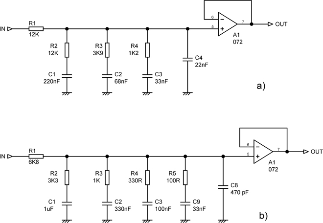
Figure 24.33 Two -3 dB/octave pinkening filters for turning white noise into pink noise.

Figure 24.34 The simulated response of the 4x RC -3 dB/octave filter in Figure 24.33b. The error trace at top (multiplied by 10) shows a maximum error of +0.28 dB over the 20 Hz–20 kHz range.
The response of b), the more expensive and more accurate version, is shown in Figure 24.34. The measured curve is seen to be closely parallel to the -3 dB/octave line drawn below it on the graph. A still more accurate -3 dB/octave filter can be made by using seven RC networks that fit in with the E6 capacitor series; accuracy is within ± 0.1 dB over a 10 Hz–20 kHz frequency range. For this and a great deal more on pinkening filters, and other filters with non–6dB slopes, see my book The Design of Active Crossovers. [10] You need the second edition.
Red noise is rarely required, but if needed, it can be made from white noise by passing it through a simple integrator, which has the necessary -6 dB/octave slope. Some sort of DC feedback will be required to stop the integrator output drifting.
References
[1] Self, Douglas “A High-quality Compressor/Limiter” Wireless World, Dec 1975, p 587
[2] Duncan, Ben “VCAs Investigated” parts 1–3, Studio Sound, Jun–Aug 1989
[3] Buff, Paul (Allison Research) “The New VCA Technology” db, Aug 1980, p 32
[4] Bransbury, Robin “Automation and the VCA” Studio Sound, Aug 1985, p 80
[5] Frey, Douglas “The Ultimate VCA” AES preprint
[6] Hawksford, Malcolm “Topological Enhancements of Translinear Two-quadrant Gain Cells” JAES, Jun 1989, p 465
[7] Shorter, et al. “The Dynamic Characteristics of Limiters for Sound Programme Circuits” BBC Engineering Monograph, No. 70, Oct 1967
[8] Self, Douglas The Audio Power Amplifier Design Handbook 6th edition. Newnes, 2013, p 270
[9] Self, Douglas Ibid, p 39
[10] Self, Douglas The Design of Active Crossovers 2nd edition. Focal Press, 2018, pp 415–421