5
Architectures with Bus-Based Switch Fabrics: Case Study—Decnis 500/600 Multiprotocol Bridge/Router
5.1 Introduction
The DEC Network Integration Server 500 and 600 (DECNIS 500/600), developed by Digital Equipment Corporation (also known as DEC or Digital), are examples of the earlier first-generation switch/routers that integrated (multiprotocol) Layer 3 forwarding (routing), Layer 2 forwarding (bridging), and network gateway functions on a single platform [BRYAN93, COBBGR93]. These devices offered multilayer switching over a number of LAN and WAN interface types available at that time.
The DECNIS 500/600 was developed in the early 1990s during the era of multiprotocol networking (IP, IPX, AppleTalk, FDDI, X.25, etc.) and when switches and routers were mostly implemented in software. The DECNIS 500/600 was designed to be flexible enough to support a wide range of Layer 2 and 3 functionalities while offering high forwarding performance. This chapter describes the architecture and implementation of the DECNIS 500/600 switch/route along with the main ideas that influenced the design of this family of switch/routers.
To achieve high packet forwarding performance, the DECNIS 500/600 employed a centralized forwarding engine assisted by distributed forwarding algorithms and buffer management mechanisms implemented on the line cards. This method of centralized forwarding, where only packet headers are sent to the centralized forwarding engine, and actual packet forwarding performed by the line cards is referred to as “in-place packet forwarding.” Packet forwarding to the destination line card(s) is performed by the source line card assisted by memory components it supports. The discussion includes a description of the packet forwarding processes in the line cards.
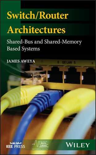
Based on the architecture categories defined in Chapter 3, the architectures discussed here fall under “Architectures with Bus-Based Switch Fabrics and Centralized Forwarding Engines” (see Figure 5.1).

Figure 5.1 Bus-based architecture with forwarding engine in centralized processor.
5.2 In-Place Packet Forwarding in Line Cards
The first generation of routers and switch/routers performed longest prefix matching lookups in software, mainly due to the complexity of the IP forwarding table lookup process. Software-based lookups, however, limited the overall packet forwarding rates of a routing device, especially when the device supports high-speed interfaces. This limitation drove routing equipment vendors to develop other techniques to improve packet forwarding even if the device uses a centralized forwarding engine.
One such forwarding method is to allow the inbound network interface (or line card) to forward only the packet header of the incoming packet to the centralized forwarding engine. The forwarding engine processes the packet header (forwarding table lookup, TTL update, IP header checksum update, Ethernet checksum update, etc.) and then instructs the inbound interface to forward the packet (along with a modified packet header) to the correct outbound interface(s) (Figure 5.2). This forwarding approach (in-place packet forwarding) improves system performance by reducing the amount of data transfers that can take place across the (bus-based) switch fabric. Data transfer over the shared bus is often the major factor that limits performance in bus-based devices).

Figure 5.2 In-place packet forwarding.
As described in previous chapters, another approach is to allow a forwarding engine to maintain a route/flow cache of frequently used destination addresses that can be used as a front-end lookup table. This front-end table is consulted first before the main forwarding table any time a packet arrives. Several architectures have been proposed over the years that allow for exact match searches to be performed in hardware within the route/flow cache. In this case, if a destination address is matched by the route/flow search, the packet can be forwarded immediately instead of being sent for the more complex longest prefix matching lookup. These improved architectures are described in various chapters of this book.
Higher performing designs decouple the routing and management processing (control plane) from the actual packet forwarding processing (data plane). Separation of the control and forwarding planes is achieved by allowing a system to have two independent processing modules, a routing and management engine (also called the route processor) and a packet forwarding engine. With this decoupling, the control plane and data plane functions are assigned to these separate engines or processors. The forwarding engine handles the actual packet forwarding, while the route processor is responsible for running the routing protocols and generating the routing and forwarding tables used by the forwarding engine.
5.3 Main Architectural Features of the Decnis 500/600
The DECNIS 500/600 architecture (described in [BRYA93] and illustrated in Figure 5.3) consists of a bus-based backplane (Futurebus+) along with its associated interface circuitry, a control CPU card (Management Process Card (MPC)) that supports the core control plane functions, a number of network interface cards (line cards), and a packet memory card (Packet Random-Access Memory (PRAM) card). The PRAM card in turn contains a centralized forwarding engine (Address Resolution Engine (ARE)) that is responsible for Layer 2 and Layer 3 forwarding of packets.

Figure 5.3 High-level view of an architecture with packet header-copy forwarding.
The central packet memory (PRAM) is organized in units of 256 byte buffers, and is shared among all the network interface cards. The DECNIS 600 supports seven line card slots, while the smaller DECNIS 500 supports only two line card slots. The PRAM is the module in which packets transiting or destined to the switch/router itself are stored. Buffer ownership is transferred from one network interface card to another by a swap process (where a full buffer is exchanged for an empty one).
The purpose of the buffer management mechanism is to govern and improve the performance of the transfer mechanism (handling buffer ownership), in addition to providing buffer allocation fairness. To allow efficient storage of data, the system uses fractional buffers much smaller than the maximum packet size (maximum transmission unit (MTU)) of the network interfaces in the system. The system is designed to allow applications to run from local memory supported on the line cards and the MPC. As will be discussed below, the line cards support processors to allow some packet forwarding functions to be performed locally.
The DECNIS 500/600 was designed to allow forwarding of packets directly between the line cards (once the forwarding table lookups are completed by the ARE) in order to maximize packet forwarding performance. The line cards support functions that allow Layer 3 forwarding on the line card (for a number of Layer 3 routing protocols, for example, IP and IPX) as well as Layer 2 forwarding for other Layer 2 traffic (e.g., Ethernet, FDDI). The management processor runs the software that controls the system, including initialization and start-up of the line cards, generating and exchanging routing and bridging protocol messages, construction and maintenance of the Layer 3 and Layer 2 tables, and network management.
5.4 Decnic 500/600 Forwarding Philosophy
When forwarding a Layer 3 (routed) packet, the incoming packet at a network interface is logically viewed to consist of three parts: the data link header, the Layer 3 header, and the packet payload (body). The receive process (RXP) shown in Figure 5.3 examines the data link layer information in the arriving packet and extracts the data link header from the packet. The RXP then parses and copies the Layer 3 header into the packet memory (PRAM) without modifying it.
Any required modifications on the Layer 3 header are carried out after the Layer 3 forwarding decision is made (by the ARE) and when the packet is ready to be transmitted. The modification information to be written in the packet is carried in a data structure called a packet descriptor (Figure 5.3). The packet descriptor occupies space reserved at the front of the allocated first packet buffer space. Recall that the PRAM is organized in units of 256 byte buffers. The packet payload is copied into packet buffers in the PRAM, using up packet buffers as required.
After the destination IP address is copied to the ARE for forwarding table lookup, the receive process is free to start processing another incoming packet. Meanwhile, the ARE completes the forwarding table lookup process, after which the receive process reads from the ARE the forwarding parameters needed to complete the processing and forwarding of the packet. The forwarding parameters provide to the RXP information about the packet's outbound port and channel (at the output line card), the data link address for the next hop, and any packet rewrite information required for forwarding. The receive process adds the forwarding information received from the ARE to the information saved from parsing the arriving packet to construct the packet descriptor in packet memory (PRAM) (Figure 5.3).
The receive process constructs a set of ring vectors for the ARE-processed packet, one ring vector for each (256 byte) packet buffer used to store the packet. Each ring vector holds a pointer to the (256 byte) packet memory (PRAM) buffer used, in addition to other information used to determine to which priority queue the packet buffer should be assigned as well as to determine the packet's relative priority in the system. When congestion occurs, the additional ring vector information (that carries the packet's priority) is used by the network interface cards to discard the low-priority packets first.
The ring vectors associated with the processed packet are then sent to the transmit process (TXP) on the output network interface card, which then queues them (locally) to be transmitted to the next hop. To begin the process of preparing the packet for transmission, the TXP first reads the packet descriptor from its location in the first packet memory (PRAM) buffer. The information in the packet descriptor is used by the transmit process to build (rewrite) the new data link header, update relevant fields in the Layer 3 header, and update other fields in the header (e.g., quality-of-service fields) without the TXP having to reparse the packet header. The transmit process rewrites the data link header, reads the Layer 3 (routing) header from the packet memory and performs the appropriate updates, and then fully constructs the packet by reading the packet payload (body) from packet memory.
The Layer 2 forwarding process in the DECNIS 500/600 operates in a fashion similar to the Layer 3 forwarding process, except that the data link header in the arriving packet is retained from inbound port to outbound port. The Layer 2 forwarding process requires parsing only the data link header from the arriving packet.
5.5 Detail System Architecture
To develop the DECNIS 500/600 as a high-performance switch/router with the technology available at that time, the functional requirements of the switch/router were split into two parts: requirements best handled centrally and those best handled in a distributed fashion.
- Distributed Functions: The data link (Layer 2) and network layer (Layer 3) forwarding functions present the main and highest processing load on the actual data path (plane). These functions operate almost totally in a local context, which allows them to be distributed and assigned to a processor associated with a line card or a group of line cards. These data path functions have processing requirements that scale linearly with both network interface speed and number of network interfaces supported by the system. However, some aspects of these per network interface functions, such as initialization of link/line card and processing of control and exception (special) packets, are more efficiently handled only centrally where a more sophisticated processing environment can be created for them. For this reason, these functions can be decoupled from the critical data path processing and placed in a centralized processing module.
- Centralized Functions: In contrast to the data plane functions that can be distributed and handled in the line cards, the control and management functions of the system, including the running of the routing protocols and construction of the routing and forwarding tables, are best handled in a centralized module. This is because these are system-wide functions and processes that operate in the context of the switch/router as a whole. The processing requirements associated with these functions are proportional to the size of the network and not to the speed of the network interfaces. Network routing protocols are typically designed to generate a lower amount of traffic (compared to end-user traffic), thereby presenting lower processing loads in routers and switch/routers. The routing protocols have designs that minimize control traffic loads and bandwidth, thereby allowing the construction of relatively simple, low-performance control traffic processing modules in the routing devices.
The above processing considerations resulted in a DECNIS 500/600 architecture that has a central management processor (the MPU) and a set of per line card forwarding processors (for in-place packet forwarding). Each line card communicates on a peer-to-peer basis with other line cards to forward the normal packets transiting the system (that make up the majority of the network traffic).
The management processor behaves, in essence, like a normal full-blown switch/router, except that its participation in packet forwarding is limited to control and management packets. With the system functions properly split between the peer-to-peer line card forwarding processors and the MPU, a buffer and control system was designed to efficiently couple these system processors together.
5.5.1 Centralized System Resources
The DECNIS 500/600 employs three centralized resources: MPC, PRAM, and ARE (Figures 5.3 and 5.4). The decision to centralize these resources was based solely on reducing both the cost and the complexity of the system. The DECNIS 500/600 was designed to use a partially centralized architecture in which only one processor (the management processor in the MPC) plays the role of the route processor (control engine) as in the traditional router sense. This central processor is responsible for running the routing protocols and building the routing and forwarding tables, network management, and being a central repository for the whole switch/router. The peripheral processors in the line cards will then be responsible for the majority of the actual packet forwarding work.
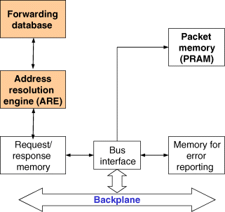
Figure 5.4 Packet Memory (PRAM) and Address Resolution Engine (ARE) card.
5.5.1.1 Management Processor Card (MPC)
The MPC is the entity that supports all the routing, control, and management software functionality necessary to tie together the collection of forwarding agents located on the line cards (to form a stand-alone switch/router). The system appears to the rest of the network, from a Layer 3 forwarding perspective, indistinguishable from a traditional router. The processing and memory capabilities of the MPC are designed to be those associated with a typical switch/router.
The MPC (or route processor card) was designed to support two processors: a VAX device that serves as the main processor and a uniprocessor model for the common Futurebus+ based backplane interface. The main MPC processor is responsible for overall control and command of the DECNIS 500/600 system and provides all the control, management, and packet forwarding functions typically found in a monoprocessor switch/router or router. The DECNIS 500/600 uses a backplane with 16 bit processor interfaces designed with self-contained functionalities that free the main MPC processor from performing time-critical backplane-associated tasks.
There are a number of (special) packet types (control, management, and exception packets) that are sent directly to the control/management CPU (MPC) for processing. For example, the receive process (RXP) may receive a packet in error or it cannot process a packet with IP header option that requires additional information (i.e., a system context) to process, or a packet that is addressed to the DECNIS 500/600 switch/router itself (including certain multicast packets). The RXP queues such packets to the management processor (control CPU) in exactly the same way it would queue a packet for transmission by a transmit process. The management processor supports a full-function switch/router that is able to handle these special packet types. Similarly, packets sent by the management processor are queued and presented to the appropriate TXP in exactly the same way as an RXP.
When a network interface card receives a packet destined to the MPC, it inspects the packet and informs the MPC whether it is data, routing (Layer 3) control, bridging (Layer 2) control, or system control information (which includes responses from the line card to commands from the MPC). Queues are used at all the network interfaces within the DECNIS 500/600 switch/router. An MPC “assistance processor” identifies the different messages types and queues them on separate internal queues.
Switch/routers must allocate sufficient buffering to handle the routing control messages that they receive and process. Consequently, the DECNIS 500/600 implements a buffer ownership scheme to guarantee the buffering requirements for control messages. To maintain buffering for control messages, the control CPU also implements a mechanism for buffer swapping between the data link and routing modules, as illustrated in Figure 5.5.

Figure 5.5 Buffer swapping between data link and routing modules.
The DECNIS 500/600 must guarantee that the data link layer (in the line cards) does not run out of buffers; otherwise, control messages that are regarded as very important for routing and control functions will not be received by the MPC. To ensure that the data link layer always has an adequate number of buffers, the control CPU assigns the data link a fixed number of buffers that is maintained at all times.
Each time a packet buffer is transferred from the data link module (in the line card) to the routing/control engine (in the MPC), another buffer (a free buffer) is transferred back to the data link module to replace it. If the routing/control engine finds that it has no free buffers to swap, it selects a less important packet, frees up the buffer contents, and passes that buffer to the data link module. This ensures that the data link layer always has buffers for local use. The DECNIS 500/600 line cards also support similar arrangements for line card-to-line card communication.
5.5.1.2 Packet Random-Access Memory
The DECNIS 500/600 was designed to have sufficient shared bus bandwidth to allow the use of a single centralized shared buffer memory (PRAM) for packet storage in the system. This approach, however, causes every incoming packet to cross the shared bus twice, resulting in some loss in bus bandwidth utilization.
5.5.1.3 Address Resolution Engine
The designers of the DECNIS 500/600 analyzed the processing power needed to parse incoming packets and perform the lookup of the destination network address (in a centralized forwarding engine (ARE)) and concluded that the line cards would need some form of assistance if the processing requirements associated with each line card and the ARE was to be made reasonably cost-effective. At the time of the DECNIS 500/600 development, there were already some advancements in the design of hardware forwarding/search engines that made it possible to design a single address parser and lookup engine powerful enough to be shared among all the line cards.
This forwarding engine (ARE) was powerful enough to parse the complex structure of an IP packet (and other protocol packet types) and perform the longest match prefix lookup. In addition, with the DECNIS 500/600 being a multiprotocol switch/router, the forwarding engine was designed to cope with the other routing protocol address formats and the Layer 2 address learning and forwarding requirements of transparent bridging. Also, by centralizing the Layer 2 and 3 forwarding tables, the designers reduced the cost and board area requirements of the line cards and avoided the processing and shared bus (Futurebus+) overhead associated with maintaining several distributed forwarding tables (in the line cards).
Figure 5.6 presents a block diagram of the packet memory (PRAM) and ARE card. As illustrated in this figure, incoming packets and related data and the forwarding tables associated with the ARE are stored in separate dynamic RAM (DRAM) arrays. The ring vector data structures are stored in static memory and are used by the network interface cards to post requests and read responses from the ARE. The ARE was developed as a special ASIC and included some of the other control logic required for the other modules on the card such as the synchronous portion of the Futurebus+ backplane interface and PRAM refresh control.

Figure 5.6 Bus interface of DECNIS switch/router.
The ARE (which serves as the forwarding engine in the DECNIS 500/600) provides the necessary hardware assistance required in packet parsing and destination address lookups. This single ARE is shared among all line cards in the system. The ARE has sufficient capacity to support a DECNIS 600 switch/router fully populated with line cards that support interfaces each with a bandwidth of up to 2 × 10 Mb/s. However, beyond this link speed, local destination address (or route) caches have to be used in the line cards. It was determined that the shared bus bandwidth and forwarding table lookup rate required to support multiple fiber distributed data interface (FDDI) line cards would place an excessive processing load on the system. So, to support FDDI line cards, the system was equipped with the central ARE forwarding engine assisted by a line card-resident destination address (route) cache.
5.5.2 Backplane and Interface Logic
The backplanes used in DECNIS 500/600 are based on the Futurebus+ standard (IEEE Standard for Futurebus+: Logical Protocol Specification (IEEE 896.1-1991) and IEEE Standard Backplane Bus Specification for Multiprocessor Architectures: Futurebus+ (IEEE 896.2-1991)). The backplane employs 2.1 V terminated backplane transceiver logic (BTL) (IEEE Standard for Electrical Characteristics of Backplane Transceiver Logic (BTL) Interface Circuits (IEEE 1194.1-1991)). The DECNIS 500 line cards used 32 bit data and address paths, while the DECNIS 600 backplane was designed to use 64 bits.
In all modules except the PRAM card (which also holds the ARE), the basic backplane interface (shown in Figure 5.6) consists of two ASICs (bus control ASIC and data path ASIC), BTL transceivers, and a number of local memory and registers. These two backplane ASICs are shown in Figure 5.6. The bus control ASIC is responsible for handling bus access requests via a central bus arbitration mechanism, controlling the backplane transceivers and running the parallel protocol state machines for backplane access. The data path ASIC, on the other hand, has two 16 bit processor interfaces (Ports R and T as shown in Figure 5.6), several DMA (direct memory access) channels for each processor port, backplane address decode logic, byte packing/unpacking, and checksum and FCS (frame check sequence) support.
Four DMA channels are provided on the backplane for each processor port. Two of these DMA channels support full-duplex data paths, while the remaining two DMA channels (which are optimized for bulk data transfer) are double-buffered and are configurable to operate in either direction (half-duplex or simplex transmission at a time). As soon as a block fills up, DMA write transfers then occur automatically. Similarly, on suitably configured empty blocks, DMA prefetch reads also occur automatically. The two double-buffered DMA channels (configurable to be half-duplex) are provided in the system to allow bus transactions to take place simultaneously (in parallel) with processor access to the other block.
Data transfers between a processor and any one of the four DMA channels (two full-duplex and two half-duplex channels) are carried out under direct control of the processor, where the processor reads or writes every byte of data to or from the DMA streams. This direct control arrangement provides a great benefit in that it simplifies the design of the related hardware and avoids the need for ASIC DMA support on the processor buses. More importantly, by using processor read and write cycles, the behavior of the system is made deterministic, and furthermore this ensures that the processor has the correct context when all operations have been executed to completion, regardless of the outcome.
The data path ASIC, as illustrated in Figure 5.6, also supports a boot read-only memory (ROM), ring vector memory (RVMEM), command/status registers (CSRs), the geographical address, a local bus containing the control interface for the second bus control ASIC, and nonvolatile RAM (NVRAM) for error reporting. The system is designed to allow a number of the CSRs and the RVMEM to be accessible via the Futurebus+ based backplane.
Another important feature noteworthy is that all resources can be accessed from either of the two 16 bit processor interfaces (Ports R and T). The data path ASIC allows the various subsystems to arbitrate internally for shared resources and is equipped with a number of other features that assist to make data transfers more efficient, for example, a summary register that stores write activity to the RVMEM.
The data path ASIC can be operated/driven from one 16 bit processor interface (Port T). It can be used in the implementation of low-speed line cards that have a relatively simple design. Furthermore, the backplane interface logic contains two (i.e., primary and secondary) data path ASICs (as shown in Figure 5.6) that are served by a common bus control ASIC connected to the primary data path ASIC's local bus. The primary and secondary data path ASICs each takes on a unique device/node identifier in the address space of the backplane. The backplane also provides dedicated lines for temperature sensing, power status, and other system conditions.
5.5.3 Line Cards
The DECNIS 500/600 supports FDDI and Ethernet network adapters as well as synchronous communications interfaces that all use different adaptations of the standard Futurebus+ shared bus backplane interface.
5.5.3.1 Ethernet and FDDI Adapters
A number of Ethernet adapters were developed for the DECNIS 50/600. A single-port 10BASE5 (Thickwire) Ethernet adapter was developed that employs a dual-processor architecture (Ports R and T on the primary data path ASIC in Figure 5.6) to interconnect the Ethernet adapter and its associated buffer (tank) memory. This adapter was reworked to place the tank memory interface (TMI) into an ASIC, resulting in a dual-port adapter version. This adapter version was a full remake of the bus backplane interface logic of the DECNIS 500/600 presented in Figure 5.6 but designed to include two Ethernet ports. This adapter was developed in two versions supporting 10BASE5 (Thickwire) and 10BASE2 (Thinwire) Ethernet technologies.
The DEC FDDIcontroller 621 is an FDDI adapter and has an architecture as shown in Figure 5.7. This adapter was developed as a two-module unit to handle the high packet filtering and forwarding rates required for FDDI. The FDDI adapter hardware contains a packet filtering engine (Figure 5.7) closely coupled to a line interface unit supporting FDDI interface functionality, a synchronous interconnect between the two submodules in the cards, and a multichannel DMA engine for data transfer through the adapter.

Figure 5.7 Line card and system interface architecture.
The DEC FDDIcontroller 621 adapter's DMA engine (in the system interface module (Figure 5.7)) accesses the tank memory under the control of the RISC (reduced instruction set computing) processor, and it can be set up and monitored with very little processor overhead. The system transfers packet data to or from buffers in the packet memory (PRAM) to the tank memory in the line card, where whole packets are maintained in contiguous tank memory address space. A second DMA channel on the network adapter allows the transfers of full packets (in a single burst) to or from the buffer memory located on the line interface submodule of the line card.
The line cards were designed to allow traffic processing between the buffer memory (in the line interface submodule) and the ring vectors to be done in hardware. An additional (third) DMA channel was included to allow prefetching packet header information held in the tank memory (in the system interface submodule in Figure 5.7) and then burst transferring it into the RISC processor subsystem for packet processing.
The DMA engine (also shown in the system interface submodule in Figure 5.7) contains a tank memory arbitration mechanism and is capable of queuing multiple commands in addition to operating all DMA channels supported in parallel. The 32 bit RISC processor subsystem (in the system interface submodule in Figure 5.7) is responsible for the line card processing, as well as communicating with the standard bus interface processor via a dual-ported RAM.
5.5.3.2 Synchronous Communications Interfaces
The DECNIS 500/600 supported two synchronous communication wide area network (WAN) adapters. One is a 2.048 Mb/s two-line WAN adapter. The other is a WAN device supporting up to eight lines with each line running a reduced line rate of 128 kb/s. All the lines in two WAN adapters are full duplex with modem control.
The eight-line (128 kb/s) synchronous communication adapter employs a uniprocessor architecture plus three industry standard serial communications controllers (SCCs). A 2 m cable connects the clocks and data associated with the lines/channels, as well as one more channel that carries multiplexed modem control information, to a remote distribution panel. Remote distribution panels were designed to support the eight lines (in the eight-line 128 kb/s WAN adapter) using the V.35, EIA422, or RS232 electrical interface standards. A four-line multiple standard panel with a reduced fan-out was also developed that allowed mixed (V.35, EIA422, or RS232) electrical interfaces from a single synchronous communications WAN adapter. This multistandard remote distribution panel used a 50-pin cable also employed in the other communication products from DEC.
The two-line synchronous communication WAN adapter, on the other hand, employed a four-processor interface, as illustrated in Figures 5.6 and 5.8. The SCC was developed as an ASIC module tailored for the specific form of data-flow processing used in the DECNIS 500/600 architecture. The SCC was closely linked in design to the functioning of the data path ASIC of the backplane interface logic (Figure 5.6) and its associated processors to allow optimal and efficient data transfer.

Figure 5.8 Block diagram of the DEC WANcontroller 622 adapter.
The design of the two-line WAN adapter hardware resulted in minimal dependency between the data receive and transmit tasks. This was done by recognizing and taking advantage of the limited coupling that exists in acknowledged data link protocols such as HDLC (high-level data link control). The processors exchange state information via a small two-ported RAM located in the WAN adapter's SCC. Two 50-pin V.35 and EIA422 interfaces were provided on the WAN adapter.
5.5.4 Buffer System
Figure 5.9 is a schematic diagram of the buffer system and buffer ownership transfer mechanism of the DECNIS 500/600. The receive processes (RXPs) are allocated only sufficient buffering to handle the data transfer latencies that can occur during the various processing stages of packet forwarding in the system. The longest duration of packet storage (i.e., time being held in buffers) occurs while a packet is owned by the transmit process (TXP).

Figure 5.9 Buffer transfer scheme: buffer ownership movement.
When a receive process (RXP) completes processing a packet that is destined for a particular destination transmit process (TXP), it swaps the PRAM buffers where the packet is stored for the same number of empty buffers owned by that TXP. It is only when the TXP is able to replace the RXP's packet buffers with empty buffers it owns does the actual buffer ownership transfer take place. If the swap of buffers (between the RXP and TXP) cannot be completed due to the TXP lacking free buffers, the RXP reuses the packet buffers it is currently holding for another incoming packet. This is to prevent a TXP from accumulating buffers and thereby preventing a RXP from receiving and processing incoming packets destined for other output ports.
Designing an efficient buffer ownership transfer scheme was an important part of the development of DECNIS 500/600. The buffer transfer scheme uses a number of single writer/single reader ring vectors (simply referred to as rings), with one ring vector assigned to each RXP and TXP pair (i.e., pairwise) swap of buffer ownership that can occur in the system. With this arrangement, each TXP is assigned one ring vector for each of the RXPs in the system (including the TXP itself), in addition to one ring vector that is reserved for the control CPU (i.e., the management processor).
Whenever an RXP has a packet buffer to exchange (or swap) with a destination TXP, it begins by reading the next (buffer) transfer location in its ring vector (set of pointers) that is associated with (i.e., corresponding to) that TXP. If the RXP finds that the TXP has a free buffer, the RXP swaps that free buffer with the packet buffer it wants to send – thereby keeping the TXP's free buffer as a replacement for the packet buffer. The information involved in the buffer ownership transfer consists of a pointer to the packet buffer, status of buffer ownership, and information that indicates the type of data stored in the packet buffer. The data structure used in the process is a ring vector, and to indicate/specify a ring vector's transfer of ownership, a single-bit semaphore (i.e., to control access to the ring vector) is used.
Figure 5.9 can be used to illustrate how the buffer ownership transfer scheme works. As already described, each transmit process (TXP A or TXP B) has a ring vector dedicated to each of the receive processes in the system (RXP A and RXP B). The process RXP A swaps ring vectors to “Ring A” associated with TXP A and TXP B, and RXP B swaps ring vectors to the “Ring B” associated with TXP A and TXP B.
As the process of buffer ownership transfer takes place, the TXP executes a scavenge process, which scans all the ring vectors associated with it for new packet holding buffers (i.e., buffers with incoming packets). The TXP then queues these packet buffers (specified by the ring vector) in the transmit queues (TXQs). The TXP also replaces the (queued up) entries in the ring vector with entries from its local free buffer list (Figure 5.9). The buffered data-type information enables the TXP in the destination transmit line card to immediately determine the relative priority of the data held in the packet buffer. With this, if the destination line card runs out of buffers due to system overload or congestion, it will be able to discard low-priority packets in order to preserve network stability.
The encodings in the ring vector were optimized to compact the ring vector swap transaction. This was to allow, for all unicast traffic, a single longword read (for new packet carrying buffers) followed by a single longword write (for free buffers) for each buffer ownership exchange or swap. To handle multicast traffic, the DECNIS 500/600 uses a second longword. To reduce the (TXP) processing time associated with running the scavenge process and the amount of traffic that traverses the shared bus of the DECNIS 500/600, the RAM in which the ring vectors are held is placed on the transmit side of a line card. Appropriate hardware is included to watch for activity in the ring vectors so that they can be reported to the TXP.
To allow efficient use of PRAM resources, long packets are fragmented and stored over a number of buffers. The unit buffer size (of 256 bytes) achieved a better compromise between memory use efficiency and processing overhead associated with buffer management. This buffer size compromise may lead to a fraction of the arriving packets stored over more than a single buffer. This means that when an output port on a line card goes into congestion, it is no longer certain that a complete set of packet buffers (for a full packet) will be swapped.
Therefore, the system ensures that a processed packet is queued for transmission in the transmit queues (TXQs) only if it has been fully transferred to the transmit process (TXP) on the destination line card. To handle dissimilar scavenge and swap process speeds, the transfer of buffers (between an RXP and a TXP) is staged using a process called binning. In this process, a TXP obtains a complete set of packet buffers (holding a full packet) from an RXP before queuing the packet for transmission in the TXQs. This prevents a partial packet buffer transfer due to system overload (or congestion) or a slow receive process (RXP) from impeding or blocking the progress of data transfer on other ports in the system.
Layer 2 forwarding (transparent bridging) in the DECNIS 500/600 requires a mechanism to support the forwarding of flooded and multicast packets to multiple destination output ports. In some architectures, the flooding and multicasting to multiple ports is performed by replicating a single packet using a copying process. Other architectures handle this process using a central multicast service. Using a central multicast service can result in synchronization issues when a destination Layer 2 address transitions from the unknown address to the learned address state.
The designers of the DECNIS 500/600 realized that packet replication by the line cards was not practical since the line cards do not keep a local copy of an arriving packet after it has been copied to the central packet memory (PRAM). The solution was therefore to employ a system in which multicast designated packet buffers are loaned to all the destination transmit line cards. The system used a “scoreboard” (that indicates outstanding buffers loaned) to record the state of each multicast buffer.
When a loaned multicast buffer is returned from all its destination transmit line cards, the buffer is appended/added to the multicast free buffer list (or queue) and becomes available for reuse. The multicast buffer loan and return processes are similar to the normal unicast packet buffer scavenge and swap process described above, with the addition that the ring vector used is extended slightly to include the information needed for rapidly getting the data that are stored in the memory location pointed to by the ring vector (pointer).
5.5.5 DECNIS 500/600 Software Architecture
In this section, we discuss the software architecture of the DECNIS 500/600. We discuss first the software architecture of the management processor (in the MPC) followed by the software architecture of the receiver and transmitter in a line card. The discussion is followed by details on how the system forwards multicast packets.
Figure 5.10 illustrates the software architecture of the MPC in the DECNIS 500/600. The software allows the MPC to act as a full-function switch/router and X.25 gateway on its own. The architecture also includes adaptation software layer necessary to hide the details of the DECNIS 500/600 MPC software environment from the details of the line cards.

Figure 5.10 Software structure in the management processor card.
The control and management part of the system software code includes the Layer 3 (routing), Layer 2 (bridging), network management, and X.25 software. This code was derived from the software used in the Digital's WANrouter 500 (an extended version of the software used in that device). The software extensions included in the DECNIS 500/600 code version were important to supply Layers 2 and 3 forwarding table updates and system configuration information to the adjacent DECNIS 500/600 environment adaptation module. The environment adaptation module hides the control and system management module from the details of the forwarding functionality in the line cards.
The DECNIS 500/600 environment adaptation module (Figure 5.10) contains key system software code components that are responsible for line card data link initialization, line card control code, and the software code needed to transform the Layer 2 and 3 forwarding table updates into appropriate data structures used by the ARE. The DECNIS 500/600 environment adaptation module has another important software component that handles the scavenge and swap packet buffer functions required for communication with the RXPs and TXPs in the line cards. These scavenge and swap functions have real-time operating constraints associated with them, thereby requiring them to be split between an assist processor (not depicted) and the management processor on the MPC.
The control and management software code module (Figure 5.10) was designed to allow the management processor in the MPC to function as full-fledged switch/router and also to allow the introduction of new functionality in the DECNIS 500/600 in stages. Whenever the need for a new protocol type in the system arises, this feature can be initially implemented and executed in the management processor, and with the line cards providing the required data link framing and network interface service. This allows the DECNIS 500/600 at a later point to move the packet forwarding functions (initially implemented in the MPC) to the line cards in order to provide a more enhanced system packet forwarding performance.
5.6 Unicast Packet Reception in a Line Card
Figure 5.11 shows the processes that run on the receive side of a network interface card. The four main processes are as follows:
- Receive process (RXP), which is the main process and aspects of which have already been described.
- Receive buffer system ARE process (RXBA), which receives inputs from the preaddress queue.
- Receive buffer system descriptor process (RXBD), which receives inputs from the receive bin queue.
- Swap process, aspects of which have also already been described.

Figure 5.11 Network interface card receive processing.
The RXP (receive process) continuously polls/interrogates the link communications controller in the line interface until it notices an arriving packet.
The RXP then fetches a pointer to a free buffer in the packet memory (PRAM) from the free buffer list queue. The RXP parses the data link header and the IP header from the arriving packet, and copies the packet byte-by-byte (as the header information is parsed) into the free buffer. The RXP determines from the data link header if the arriving packet should be Layer 3 forwarded (routed) or Layer 2 forwarded (bridged).
Once the RXP has decided the type of forwarding required for the incoming packet, the IP destination address or the destination MAC address is copied to the ARE, in addition to some information to indicate to the ARE which forwarding table to use for the lookup. The ARE incorporates some hardware to assist in the Layer 2 address (transparent) bridge learning process.
To prevent the ARE assisting hardware from accidentally learning an incorrect MAC address, the ARE is only allowed to start a MAC address lookup (in its Layer 2 forwarding table) after the RXP has completely received the packet and established that it carries a correct checksum. This restriction does not apply to Layer 3 addresses, which the ARE can look up in its Layer 3 forwarding table even before a full packet has been received, thus reducing data transfer latency.
If the packet is to be Layer 3 forwarded (the data link header is discarded), only the IP header and the packet body are copied to the buffer(s) in packet memory. The system also stores for later use the source MAC address of the incoming packet or, when the packet arrives on a multichannel line card, the channel (identifier) on which the packet was received. The system stores as well several other protocol-specific items for the packet. All this packet information is later used by the system to construct the packet descriptor.
The RXP stores the buffer pointer in the preaddress queue (shown in Figure 5.11) until the pointer can be reconciled with the result of the packet's Layer 3 destination address lookup (in the ARE's forwarding table). In the case where line card processing involves data link protocols such as HDLC (that use acknowledged data transfers), the RXP exports the latest acknowledgment status to the destination TXP.
The ARE is also polled continuously by the RXBA (receive buffer system ARE process) for the result of the forwarding table lookup (for a particular destination address), after which the RXBA stores the result in an internal data structure associated with the corresponding packet. The RXBA then moves the buffer pointer along with any additional buffer pointers to other packet buffers (used to store the remaining parts of a bigger packet) to the receive bin queue (shown in Figure 5.11).
The RXP, RXBA, and ARE forwarding engine destination address lookup processes and the link interface transmission process all operate asynchronously. This thus creates a system design in which a number of ARE forwarding table lookup results can be pending and that can also have indeterministic completion time.
The above issues can cause the reconciliation of forwarding table (destination address) lookup results for arriving packets and their associated buffers in packet memory to take place before or even after a whole packet has been received. Given that an error could occur in the arriving packet, the system was therefore designed to not take any further action on the packet until the whole packet has actually been received and all its packet buffers have been moved to the receive bin queue as shown in Figure 5.11.
The above staging process was used to avoid providing in the system a complex abort mechanism to clear/remove erroneous packets from the scavenge, swap, and transmit processes. The system was designed to have the RXBA poll the ARE at a rate of exactly one poll per forwarding table lookup request when operating under normal traffic load. With this arrangement, an ARE poll failure can increase the backlog in the preaddress queue (which holds the packet buffer pointers), but does not cause it to grow beyond two packets.
This mechanism also minimizes the shared bus (Futurebus+) bandwidth wasted in unsuccessful (or failed) ARE poll operations. However, when the line card receiver (RXP) becomes idle (with no new packets arriving), the ARE poll rate increases and the outstanding packets (in the preaddress queue shown in Figure 5.11) are rapidly processed to clear the queued/backlogged packets.
The RXBD (receive buffer system descriptor process) records the packet descriptor into the foremost part/front of the first packet memory (PRAM) buffer that is used to store the packet. The packet descriptors are protocol-specific (containing all relevant protocol information required to forward the packet) and require a callback into the corresponding protocol code to construct the descriptor.
After the packet descriptor is written into place, the buffer pointers (associated with the processed packet) are transferred to the source queue (shown in Figure 5.11), ready for forwarding (by the swap process) to the destination network interface card. The packet buffer is then swapped with the TXP in destination network interface card and the free buffer resulting is added to the free buffer queue.
5.7 Unicast Packet Transmission in a Line Card
The transmitter functions of a network interface card are shown in Figure 5.12 and consist of five processes:
- Scavenge rings process, which takes inputs from the destination rings.
- Scavenge bins process, which takes inputs from the destination bins.
- Transmit buffer system select process (TXBS), which takes inputs from the holding queues.
- Transmit process (TXP), aspects of which have already been described.
- Transmit buffer (TXB) release process, which takes inputs from the packet release queue.

Figure 5.12 Network interface card transmit processing.
The scavenge rings process is the transmit-side entity that examines/scans the swap rings (i.e., ring vectors holding pointers) for new packet buffers waiting to be queued and transmitted out of the switch/router. The scavenge process then replaces these new packet buffers with free buffers. The new packet buffers are then stored/queued in destination bins that serve as reassembly bins (one destination bin for each destination ring) in order to facilitate only full/complete packets to be queued in the subsequent holding queues.
The scavenge process first attempts to refill the destination rings with free buffers from the port-specific return queues, and if this fails, it takes the free buffers from the free list. The port-specific return queues (i.e., the MPC unicast and 16× multicast queues in Figure 5.12) are used primarily for multicast packet forwarding. The scavenge bins process inspects the destination bins to determine if they hold full packets and moves them to the appropriate (IP, bridge) holding queues. The packets are queued in the holding queues by protocol type, since different protocols have different packet fields, protocol processing requirements, and traffic characteristics.
Using round-robin scheduling, the TXBS process schedules the packets from their holding queues. The round-robin scheduling is to prevent protocols (e.g., TCP) with dynamic congestion control algorithms from being driven into congestion timeout by other protocol packet types with no congestion control mechanisms. This also allows both Layer 2 and Layer 3 protocol traffic to have a fair share of the link resources when traffic overload occurs.
The scavenge bins and TXBS processes together implement any necessary congestion-related dropping and marking of congestion bits in packets during congestion in addition to any packet aging functions. By allowing the queuing time of packets to be minimal in the receiver (side of a line card), the DECNIS 500/600 designers were able to simplify the congestion control algorithms and allow them to be executed in the transmit path.
The TXBS process selects a packet and transfers it to the TXP (via the transmit packet queue), which then transmits it to the network. TXP writes the appropriate information from the packet descriptor, rewrites the IP header, and prepends the data link header. When the TXP transmits a packet belonging to a protocol like HDLC (that uses explicit data acknowledgments), the packet is transmitted but also transferred to the pending acknowledgment queue where it waits for an acknowledgment message from the remote end.
Before the TXP transmits each packet requiring explicit acknowledgment, it examines the current acknowledgment state for the packet indicated by the remote end (receiver). The TXP may transfer packets requiring acknowledgments from the pending acknowledged queue to the packet release queue, and if it receives a retransmission request for the packet, move the packet back to the transmit packet queue.
The TXB release process removes packets (buffers) from the packet release queue and splits them into a series of queues to be used by the swap process. Buffers associated with unicast packets are placed in the free buffer list (i.e., free pool in Figure 5.12). Buffers associated with multicast packets are returned to the port-specific queue for the source network interface card, and ready to be assigned to their originating receiver (TXP). Buffers associated with packets targeted for the control and management CPU (MPC) are also queued separately in their port-specific queues.
5.8 Multicast Packet Transmission in a Line Card
A packet buffer associated with Layer 3 multicasting and Layer 2 multicasting or flooding must be transmitted by a number of line cards. This process requires the system to swap a special type of ring vector, which indicates that the buffer (for the multicast data) is only on loan to the transmitting line card, and upon completion of packet transmission must be returned to its receiver (i.e., buffer owner).
In addition to the information carried in a normal ring vector (i.e., normal packet type, buffer identification information, and fragmentation), the special (or multicast-associated) ring vector carries local referencing information, which indicates where it (the ring vector) is stored on the multicast heap. The receiver (owner) maintains a list/record of which multicast packet buffers are on loan to which transmitting line card. The scavenge process must also keep a record of which ring vector it found a particular pointer.
After transmitting a multicast packet, the TXB release process returns the ring vector to the associated (or owner) port-specific return queue. The returned ring vectors are then eventually transferred to their receiving line card (owner) through the swap process. As the owner receives these returned multicast buffers, it marks them off against the record of multicast buffers it loaned out. As soon as the receiver gets back a buffer from all transmitting line cards to which it was loaned, the buffer is returned to the free list. To allow this process to work successfully, the system reserves some buffers specifically for multicast packet forwarding.