CHAPTER 9
![]()
Analog Integrated Circuits Including Amplifiers and Voltage Regulators
In Chapter 8, we examined some simple discrete amplifier circuits. We noted that these amplifiers include characteristics of input resistance, output resistance, voltage gain, output swing, and distortion. In particular, these amplifiers have limitations of output swing when connected to a low-resistance load at Vout, and distortion with large output voltage swings.
Many of the limitations of discrete amplifiers can be reduced by using integrated circuit (IC) operational amplifiers. Also, IC amplifiers take less space and can provide lower current draw than discrete circuits. This chapter will explore some of the IC operational amplifier basic characteristics such as gain, drive capability, and power supply requirements.
In addition to IC amplifiers, we will look at voltage regulators. A voltage reference (e.g., “super Zener diode”) with a power operational amplifier generally makes up a voltage regulator that provides a constant voltage even when the current load is large (e.g., > 100 mA).
Operational Amplifiers
Operational amplifiers, or “op amps,” historically were used to solve operational math operations such as adding, subtracting, integrating (e.g., averaging), and other operations. When op amps are used with multiplying or nonlinear circuits, they can be used to find magnitudes of vectors (e.g., ![]() ), or they can be used to find an inverse function such as a log function where the original function is an exponential function.
), or they can be used to find an inverse function such as a log function where the original function is an exponential function.
In general, an op amp, when used as an amplifier has the following characteristics:
• A non-inverting input terminal.
• An inverting input terminal.
• An output terminal.
• A positive voltage power supply terminal.
• A negative voltage power supply terminal or a ground terminal.
• A negative feedback element (e.g., resistor or capacitor) that is connected to the output terminal and the inverting input terminal.
• When an op amp includes negative feedback, the voltage at the non-inverting input terminal is “equal” to the voltage at the inverting input terminal.
• The non-inverting input terminal should be connected in such a way that it provides a DC path. Generally, the non-inverting input terminal should be connected to a voltage source via a straight connection or via a resistor or inductor. Otherwise, the op amp will drift up or down in voltage until the output voltage is clipped to one of the power supplies or ground voltages.
• The inverting input terminal is connected via a resistor, inductor, and/or capacitor to the output terminal to form a negative feedback arrangement.
Operational amplifier U1 in Figure 9-1 shows an LM741 single package op amp with the non-inverting input (+) at pin 3, the inverting input (–) at pin 2, the output at pin 6 with the +V supply at pin 7 and the –V supply at pin 4. The other pins 1 and 5 are generally not used unless the user wants to adjust the input offset voltage to zero. Ideally, the op amp will have perfectly matched input transistors that result in zero volts offset at its input. Zero volts offset means if you ground both inputs, the output voltage is 0 volts. However, in practice the input offset voltage can be within ± 10 mV DC, which means if you ground the two inputs, the output pin will not be zero volts. Generally, input offset voltages are not a problem except for instrumentation and other measuring circuits where zero input offset voltage is required.
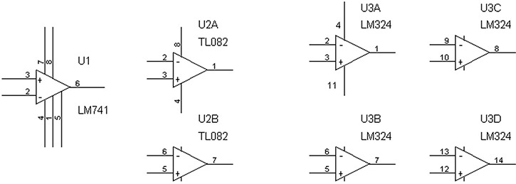
FIGURE 9.1 Op amp schematic symbols showing single, dual, and quad op amps in single packages of 8 pins (single and dual) and 14 pins (quad).
The LM741’s pin 8 is not connected. Note that U1’s power pins are 7 (+ v) and 4 (– v), with output pin 6, and input pins 2 (– input) and 3 (+ input). These pin assignments are standard for other single-package op amps such as TL081, TLC271, LF356, LF441, MC1456, and AD797.
U2A and U2B have standard pin outs for dual op amps in an 8-pin package. Here, pin 8 is the +V supply pin and pin 4 is the –V supply. Note that the power pins are at the corners of the 8-pin package, and if the IC is installed backwards (e.g., the IC is turned around), the power pins 8 and 4 will receive a reverse voltage that will damage it. If this happens, you should replace the IC and ensure that the IC’s installation orientation is correct. For the first section, pins 2 and 3 are the inverting and non-inverting input pins, while pin 1 is the output. For the second section, pins 6 and 5 are the inverting and non-inverting input pins with output pin 7. Again, these pin outs are standard for dual op amps in an 8-pin package. Thus, dual 8-pin op amps such as the LM358, LM1458, LM4558, TL082, TLC272, LF353, LF412, ISL28208, ISL28218, NJM4560, and AD712 will have the same pin outs.
For a 14-pin package, op amp sections U3A, U3B, U3C, and U3D show standard pin outs for the inverting and non-inverting input pins and corresponding output pins. Pin 4 is the +V power pin, while pin 11 is the (negative) – V power pin. Again, for the most part these are standard power pins for a quad op amp in a 14-pin package. Op amps with this pin out are LM324, TLC274, TL084, LM348. But there are exceptions such as the MC3301 quad op amp with +V at pin 14, –V at pin 7. Therefore, if you are using a quad op amp, be sure to look up the data sheet.
NOTE: Again, if the IC is turned around, the power pins will be reversed and damage will be done to the quad op amp. You will have to replace the op amp and ensure that it is installed correctly.
Figure 9-2 shows dual inline packages (DIP) for through hole and surface mount 8-pin (SO-8, small outline 8-pin) and surface mount 14-pin (SO-14, small outline 14-pin) ICs.
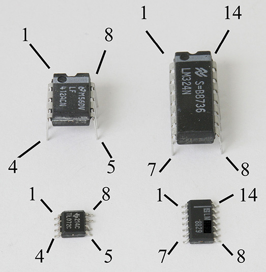
FIGURE 9.2 8- and 14-pin DIP packages on the top row and 8- and 14-pin surface mount ICs on the bottom row.
We will now show a simple unity gain amplifier known as the voltage follower amplifier. See Figures 9-3 and 9-4. The voltage follower has close to zero ohms output resistance.
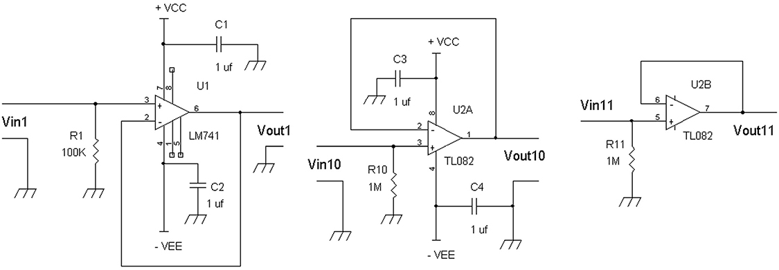
FIGURE 9.3 Voltage follower amplifiers with dual supplies with decoupling capacitors (C1, C2, C3, and C4) connected directly to the power pins to avoid oscillations from the op amps.
A voltage follower works on the negative feedback principle (Vout is connected to the inverting input). The signal voltage at the non-inverting input causes inverting input to have the same voltage. For example, in Figure 9-3 with U1, Vin1 is at pin 3 and at pin 2. But pin 6, the output pin (Vout1) is connected to pin 2 (inverting input). Thus, Vout1 = Vin1. With dual power supplies such as ± 5 volts, the voltage follower has a gain of 1 for DC and AC signals. If the input signal is a DC signal (e.g., for instrumentation), the gain is 1. For example, if Vin1 = +1.56 volt DC, then Vout1 = +1.56 volt DC. Using bipolar (plus and minus) power supplies allows a lower-frequency response down to DC because a coupling capacitor is not required. These circuits will amplify AC signals as well. So why is a voltage follower useful? If the input voltage has little capability to drive larger currents, such as driving a headphone or low-impedance load (e.g., < 1KΩ), using the voltage follower circuit allows for that. For example, if your input signal has an equivalent source resistance of 10KΩ, then only a small current (e.g., < 1 mA) will drive a 64Ω headphone, which will result in low volume. However, if you use an NJM4556 that can output up to 70 mA, driving the headphone will not be a problem.
The input resistances for each of the op amp voltage follower circuits are R1, R10, and R11, which can be changed to virtually any practical value. Thus, the input resistances of the voltage follower circuits as shown in Figure 9-3 are R1 = 100KΩ, R10 = 1MΩ, and R11 = 1MΩ. Input resistors R1, R10, and R11 can have different value resistors but we sometimes have to keep in mind the “tiny” input bias currents of the inverting and non-inverting input terminals. Input bias currents can cause a noticeable DC shift at the output when the product of the input bias and input resistors exceed 10 mV or more. If you choose an op amp that has an FET (Field Effect Transistor) input stage (e.g., TL082, LF353, TLC272), the input bias current is negligible and input resistors up to 10MΩ can be used without creating offset voltage problems.
Figure 9-4 shows a voltage follower circuit when using a single positive supply.

FIGURE 9.4 A voltage follower amplifier with a single positive voltage supply to work with AC signals.
When using a single power supply, generally, we need to create a half voltage supply to bias the input terminals and output terminal to half the supply voltage. The bias voltage, +Vb = +VCC [R10/(R10 + R11)]. Since R10 = R11, +Vb = +VCC [½]. Thus, pin 3 has the bias voltage +Vb combined with the AC portion of the Vin14. For example, if Vin14 is a 1-volt peak to peak sine wave and +VCC = 9 volts, then +Vb = 4.5 volts, and pins 3, 2, and 1 will have a composite signal of +4.5 volts DC + 1 volt peak to peak AC sinewave. The bias voltage of one half +VCC provides for the largest AC signal swing at the output (e.g., pin 1 or 7). In Figure 9-4, one of the first things to look for in single supply op amp circuits is to measure referenced to ground that the two input terminals and the output terminal are at about one-half the supply voltage.
Figure 9-4 also shows the polarity connections for polarized electrolytic capacitors C40, C50, and C60. Note the positive terminal is connected to the input and output terminals that have positive DC voltages of +VCC/2. Decoupling capacitor C30 is connected closely to pin 8, for example, within an inch to avoid parasitic oscillations from the op amp.
Also shown in Figure 9-4 is the second section of U2B that has its non-inverting input terminal pin 5 connected to U2A’s output pin 1. We can do this because pin 1 has the needed bias voltage +Vb = +VCC/2, which “automatically” correctly DC biases pin 5 of U2B. Pin 7 then provides a second or extra output signal Vout15 via C60 essentially identical to Vout14. For example, if +VCC = 12 volts, then +Vb = 6 volts DC, and if U2 = NJM4556, then we can drive two 64Ω earphones separately via Vout14 and Vout 15.
The AC input resistance with C40 being an AC short circuit, is R10 || R11, and with R10 = R11 = 200KΩ, the AC input resistance = 200KΩ || 200KΩ = 100KΩ. Again, as a reminder R11 is connected to +VCC, which serves as an AC ground. If you are only using a negative supply, see Figure 9-5.

FIGURE 9.5 A voltage follower circuit with only a single negative power supply.
In this circuit, note that the +V power pin 4 is connected to ground. We need to bias the input terminals to a voltage, –Vb such that –Vb = –VEE/2. For example, if –VEE = –5 volts, then –Vb = –2.5 volts DC.
Also, to avoid oscillations, decoupling capacitor C4 connects directly to pin 11.
A common –VEE/2 voltage source can be made with a simple voltage divider R13 and R14 and with a large value decoupling capacitor C40 as shown in Figure 9-5. C40 provides an AC short circuit to ground even at low frequencies such as 20 Hz, and it also provides an AC short circuit compared to the 100KΩ bias resistors R12 and R10. Any AC signal voltages coupled to R12 and R10 via input capacitors C70 and C90 at the input terminals of the op amps will be isolated from each other. This is because both lower connections of R12 and R10 go to C40, which is an AC short to ground. And because C40 is an AC short to ground, the AC input resistance to Vin16 is R12 (100KΩ), and the AC input resistance to Vin17 is R10 (100KΩ). Again, the (total) voltage at pins 3, 2, and 1 of U3A is –Vb plus the AC signal from Vin16. Likewise, the (total) voltage at pins 5, 6, and 7 of U3B is –Vb plus the AC signal from Vin17. Thus, the AC gain is 1. Note that –Vb can supply bias voltages via input bias resistors (e.g., 100KΩ) to the two other op amps U3C and U3D at pins 10 and 12.
In general, when making a voltage source from a resistive divider, you can scale the resistors from about 10 percent to 50 percent of the input resistors’ values, and scale the decoupling capacitor (e.g., C40) to at least ten times the capacitance of the input capacitors (e.g., C70 and C90).
Again, note the polarity of the electrolytic capacitors (e.g., C70, C80, C90, and C100) where the (–) terminals are connected to the input and output terminals of the op amps. Also the decoupling capacitor C40 has its (–) terminal connected to the voltage divider circuit R13 and R14 because R14 is connected to a negative voltage, –VEE.
The voltage follower is a unity gain amplifier that can be characterized as an amplifier with almost infinite input resistance, Rin (not counting its input biasing resistor), and nearly zero output resistance, Ro. See Figure 9-6.

FIGURE 9.6 Model of a voltage follower with plus and minus supplies.
With plus and minus power supplies, the block diagram is valid for both AC and DC signals. The input resistance is just the input resistor RA that also serves to provide a DC bias voltage (e.g., 0 volts DC) to the non-inverting input terminal of U2A. A voltage follower circuit has close to 0Ω output resistance. However, all op amps include output current limiting usually in the tens of milliamps to protect the op amp from destruction should the output terminal (e.g., pin 1) be accidentally shorted to ground.
For a single power supply where the bias voltage is provided by a voltage divider, see Figure 9-7 for the block diagram.
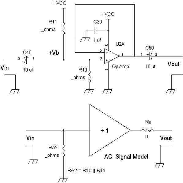
FIGURE 9.7 Block diagram of a single supply voltage follower circuit.
Because the circuit is AC coupled via input and output capacitors, C40 and C50, the block diagram refers only to AC signals for Vin and Vout. See Figure 9-7.
And as can be seen R11 is connected to the DC supply voltage +VCC that is an AC short circuit to ground. Recall that by definition a pure DC supply voltage does not include any AC voltage. Thus, the AC input resistance is R10 || R11. When +Vb = +VCC/2, R10 = R11, so the input resistance = R10 || R10 = (½) R10 or (½) R11.
The AC output impedance provided by C50 is nearly an AC short circuit and is very small when compared to the subsequent load resistance at Vout. For example, if the load resistance, RL, at Vout to ground is 2kΩ and you need the amplifier to have a good low frequency response down to 20 Hz, a good rule of thumb is to set the cut-off frequency to about one-half to one-tenth of the lowest frequency desired. In this example, we can set the cut-off frequency between 2 Hz and 10 Hz. The low-frequency cut-off frequency = 1/[2π(C50)RL] = 1/[2π(10 μf)(2kΩ)] = 7.96 Hz, which is within the range. However, electrolytic capacitors are relatively inexpensive and the cost of a 10 μf capacitor and a 33 μf capacitor is about the same. So, having C50 → 33 μf will result in a low-frequency cut-off frequency of:
(7.96 Hz)/3.3 = 2.4 Hz. The 3.3 factor comes in because 33 μf is 3.3 times 10 μf.
We will now look into some very important specifications to keep in mind when working with op amps. The voltage follower configuration will be used as an example.
Maximum Safe Power Supply Voltage
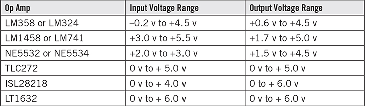
Older op amps such as the LM741, TL081, LF351 and LM318 have a 36-volt maximum across their V+ and V– terminals. Some of the newer single supply Texas Instruments LinCMOS™ amplifiers such as the TLC251or TLC271 have about a 16-volt maximum. Yet some of the newer op amps (e.g., LMV358 and NJM2100) only have a 6- or 7-volt supply limit.
See Table 9-1 on dual op amps.
TABLE 9.1 Various Op Amps with Maximum Voltage Across Their V+ and V– Supply Terminals
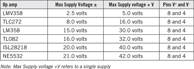
Although Table 9-1 shows the maximum supply voltages, to be on the safe side, the op amps are operated at ≤ 90 percent of maximum rated supply voltages. For example, the TLC272 would be operating with a +12-volt supply that is 4 volts below its maximum rating of 16 volts. Because not all volt meters (DVMs) are absolutely accurate, it’s always good to be on the safe side by running the op amps with a good safety margin below the maximum rated voltage.
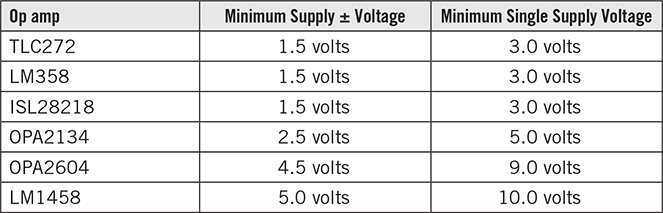
Minimum Power Supply Voltage
Not all op amp will work correctly with low-voltage power supplies, such as a single +5-volt supply or at ± 3 volts.
For example, the LM1458 or TL082 op amp will not work properly or with very poor performance (e.g., very low output swing < 2 volts p-p) when used with a +2.5-volt and –2.5-volt supply. A new op amp such as the LMV358 will work at these voltages, but a higher supply voltage such as ± 5 volts will damage it. See Table 9-2 for the manufacturer’s minimum recommended supply voltages.
TABLE 9.2 Minimum Supply Voltages for Various Op Amps Via Data Sheets
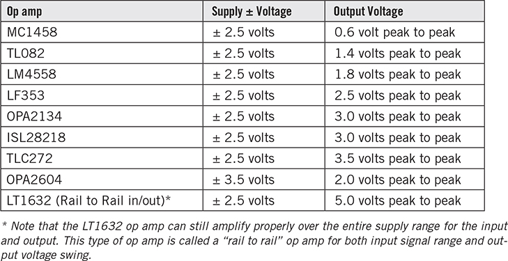
As an experiment using a voltage follower configuration (see Figure 9-6, U2A) Table 9-3 shows a summary of minimum supply voltages and their outcomes. The op amps are loaded into 10MΩ (essentially a no-load condition), and note that the results will be worse when the load resistance is 1KΩ.
TABLE 9.3 Experimental Results of Various Op Amps in Voltage Follower Configuration and with “No Load” at the Output
There are basically two types of rail to rail op amps.
• An op amp that can swing the full supply voltage range, but a smaller input range that does not match the supply voltage(s). For example, for the ISL28218 op amp, if the power supply voltage is +12 volts, the output voltage swing is 0 volts to 12 volts, but the input voltage range would be 0 volts to about 10 volts.
• An op amp that can swing the full supply voltage range that also has an input voltage range that matches the full power supply. For example, if the supply voltage is 5 volts, then the LT1632 has an input range from 0 volts to 5 volts while the output can swing from 0 volts to 5 volts also.
Caution on Providing Supply Voltages
We have to choose carefully the op amp to suit the power supply voltage or the op amp may be damaged due to overvoltage. But we must be aware of the minimum operating voltage for the op amps, or the op amp will not amplify the signal properly.
If the incoming power supply has voltage fluctuations, then we need to ensure that there is no overvoltage to the op amps. One solution is to preprocess the raw voltage into a regulated voltage using a voltage regulator integrated circuit.
For example, if you buy an unregulated wall charger DC supply that states it is a 12-volt DC 1 amp supply, usually it will provide a higher voltage (e.g., 17 volts) under a low-current load, while delivering the specified 12 volts DC at 1 amp. For safe operation, you can choose an op amp with a higher maximum voltage rating like an NE5532 that can operate up to 42 volts. Or you can use a lower-voltage op amp such as the TLC272 and regulate the “raw” voltage (e.g., a 12-volt to 17-volt range) by using an 8-volt regulator chip such as an LM7808 to provide a constant 8.0 volts to the TLC272 op amp whose maximum supply voltage is 16 volts.
Alternatively, buy a regulated wall supply, which is usually a switching power supply.
To reiterate, when powering an op amp, it is best to use some type of voltage regulation. This way, if there are spikes in the AC power line, your op amps and other circuits (e.g., logic chips) will stay protected from damage.
Voltage regulator circuits will be discussed further at the end of this chapter.
Maximum Output Current
In general, most op amps have push pull class AB output stages that provide about 10 mA of positive and negative current output. With this type of output current capability, the op amp can drive resistive load ≥ 1000Ω with ≥ 10 volts output. But this 10-mA output current can be smaller if lower supply voltages such as a single 5-volt or 7-volt supply are used.
For example, a TLC272 amplifier with a +12 volts supply in a voltage follower configuration loaded into a 220Ω resistor outputs about 5.6 volts peak to peak, whereas with a +6-volt supply, the output (before distortion) drops to 2.25 volts peak to peak.
NOTE: Trying to pull more than the maximum current results in clipping or limiting to the output voltage.
If these types of op amps that have typically a 10-mA maximum output current are used to drive low-impedance headphones such as a 16Ω or 32Ω version, signal clipping will occur.
For example, a 32Ω load is driven directly with a TLC272 with +12-volt supply with a voltage follower circuit, as shown in Figure 9-8.
FIGURE 9.8 Voltage follower circuit.
The voltage follower circuit in Figure 9-8 having a +12 volt supply and a 32Ω resistor connected to the output produces a clipped (distorted) sine wave signal as shown in Figure 9-9.

FIGURE 9.9 Waveform output with TLC272 with 5 volts peak to peak input at 1000Hz, Vin1, and 2.69 volts peak to peak output at Vout1 as measured by the dashed horizontal lines/cursors.
There are amplifiers that can supply 20 mA to 30 mA such as LM833 or NE5532 dual op amps. These can drive lower-impedance loads such as 600Ω.
A high-current op amp such as the NJM4556 can output up to ± 70 mA. This allows driving low-impedance headphones (e.g., 16Ω to 64Ω stereo headphones), or even drive small loudspeakers with a 32Ω or 50Ω impedance. See Figure 9-10, where a 32Ω load is driven with an NJM4556 using 12-volt supply with a voltage follower circuit like the one shown in Figure 9-10. The NJM4556 peak output current into 32Ω is then the peak voltage, 2.5 volts peak/32Ω or 78 mA peak.
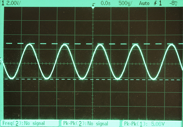
FIGURE 9.10 Waveform from NJM4556 delivers a clean sine wave with 5 volts peak to peak into 32Ω. Note that 5 volts peak to peak is the same as 2.5 volts peak.
Note that 5 volts peak to peak is equal to 2.5 volts peak.
But there is a word of warning on some op amps with very limited output current such as the LM358 and LM324 that are commonly used in DIY (do-it-yourself) projects. These op amps have very poor output drive capability. Figure 9-11 shows an LM358 with a single 5-volt supply circuit driving a 10MΩ load (see Figure 9-8, where U2A = LM358 and VCC = 5 volts, and R3 = 10MΩ or 2000Ω). With a 3000 Hz 0.5-volt peak to peak signal at Vin, see Figure 9-11 for the output waveform.
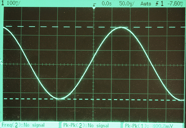
FIGURE 9.11 An LM358 voltage follower circuit’s output signal into a 10MΩ resistor with a clean 500-mV peak to peak sine wave.
However, if the LM358 voltage follower drives a 2000Ω (for R3 in Figure 9-8) instead of the previous 10MΩ, the waveform distorts quite badly. See Figure 9-12.
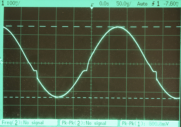
FIGURE 9.12 The LM358 voltage follower’s distorted output waveform (~ 500 mV peak to peak) when driving a 2000Ω resistor (R3). Note the discontinuities near the “zero” crossing of the sine wave. This is known as crossover distortion.
One way to reduce or eliminate the crossover distortion in an LM358 or LM324 is to connect a pull-up or pull-down resistor (e.g., 1KΩ or 1.5KΩ) from the output terminal to either the +V or –V terminal or ground terminal. See Figures 9-13 and 9-14.

FIGURE 9.13 A pull-down resistor R4' is connected from the output pin 1 to the –V or ground terminal pin 4 of the LM358 op amp to reduce or eliminate crossover distortion. Alternatively, you can use a pull-up resistor tied to pin 8 or +VCC as shown in Figure 9-14.
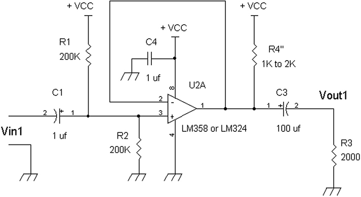
FIGURE 9.14 A pull-up resistor, R4", is connected to the LM358’s output pin 1 and pin 8 (+VCC) to reduce or eliminate crossover distortion.
The modifications via R4' and R4" in Figures 9-13 and 9-14 result in a cleaner looking sine wave as shown in Figure 9-15.
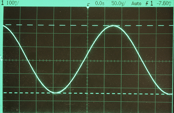
FIGURE 9.15 LM358 with a pull-down or a pull-up resistor that eliminates crossover distortion on the sine wave. The cursors with dashed lines across are also displayed for 500 mV peak to peak.
Output Voltage Range
When we supply an op amp with ± supply voltages such as ± 5 volts, we would expect that the output can swing approximately ± 5 volts. In practice, the op amp generally has a more restricted range. For example, in a TLC272 op amp, there is about a 1-volt loss from the V1 supply, but the op amp can swing almost to V–. If we use ± 5 volts, the output range is about (5 volts – 1 volt) to –5 volts, or +4 volts to –5 volts. Of course, the output range will further reduce when loaded into a resistor that draws at least 1 mA of current.
Other op amps can have more loss such as the LM 741 that loses about 2 volts on both V+ and V– supplies. For example, with a ± 9-volt power supply, the output swing is about +7 volt to –7 volts.
Special op amps that are called “rail to rail” usually provide just that—output swings that match the supply voltages. For example, an ISL28208 will provide nearly the same output swing voltages as the power supply within about 100 mV. However, because the ISL28218 op amp does not have rail to rail performance at the input terminals, when it is configured as a voltage follower the output swing will be restricted to the input range, which loses about a volt or two. For example, in Table 9-3 the ISL28218 has a swing of 3 volts with a 5-volt power supply when it is configured as a voltage follower. However, we will see later that we can take full advantage of the rail to rail output voltage range even if the input voltage range is restricted by using the amplifier as an inverting gain amplifier or as a non-inverting gain amplifier where the gain is generally ≥ 2.
Input Signal Range
Even though an op amp can swing rail to rail, that does not ensure that the input range is rail to rail. That is, if the power supply voltages are ± 5 volts, most op amps have a common mode input range that is less than or within the power supply voltages. For example, the CA3130 (Renesas) op amp can swing rail to rail at its output, but the input has a range of V– to V+ –2 volts. For a 5-volt supply where V– = ground or 0 volts and V+ = +5 volts, the input range is 0 volts to V+ –2 or 0 volts to 3 volts. So, in a voltage follower circuit even if the input signal is from 0 to 5 volts, the output will be 0 to 3 volts.
See Table 9-4 for some op amps with various output swing and input ranges for a single positive voltage supply, +V, that is referenced to ground.
TABLE 9.4 Some Op Amps’ Input and Output Voltage Ranges for a Single Supply

Let’s take examples where +V = 6.0 volts or four 1.5-volt cells connected in series.
See Table 9-5.
TABLE 9.5 Examples of Voltage Ranges Where the Single Supply Voltage Is + 6.0 Volts
A main takeaway from Tables 9-4 and 9-5 is that there are only certain types of op amps that will work well with a single 5 volt or 6 volt supply such as the LM358, ISL28218, TLC272, and LT1632. The traditional op amps used with higher supply voltages such as the LM741, LM1458, and NE5532 do not generally work at low voltages.
Also, if you notice carefully, op amps that state single supply capability have an input voltage range of at least down to ground, 0 volts, or the –V supply pin of the op amps. See the input ranges of the LM358, ISL28218, TLC272, and LT1632. The ability to “sense” input signal near ground or the –V supply of the op amp can be very handy. See Figure 9-16, where we can make a constant current circuit out of an LM358.
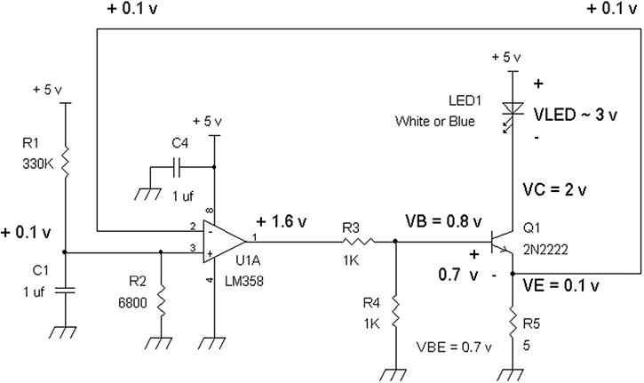
FIGURE 9.16 A feedback current source circuit with nearly 0 volt sensing at the input terminals of the LM358 op amp at pins 3 and 2.
Q1’s collector provides a constant DC current to light-emitting diode LED1 by regulating the emitter voltage, VE to 0.1 volt DC. By having emitter voltage stable at 0.1 volt the emitter current, IE, then is 0.1 volt/5Ω or IE = 20 mA. Since IE = IC, the collector current, IC = 20 mA. Since the collector is supplying current to the LED, the LED current is also 20 mA.
So, the question is how do we get a regulated 0.1 volt at the emitter? The answer is by negative feedback, which is done in the following manner:
Via voltage divider R1 and R2 with the 5-volt supply voltage, we have 0.1 volt at the (+) input of the op amp U1A. Because there is negative feedback, the (+) input terminal’s voltage at pin 3 forces the (–) input terminal’s voltage at pin 2 to be the same voltage. Thus, pin 2 has 0.1 volt. If we follow where pin 2 is connected to, pin 2 is connected to Q1’s emitter. To force the 0.1 volt at the emitter, the base voltage will have to be high enough to cause conduction in the transistor via forward biasing the base-emitter junction. The base-emitter voltage is VBE ~ 0.7 volt. So, the base voltage referenced to ground has to be VB = VBE + VE or VB = 0.7 volt + 0.1 volt. Thus, VB ~ 0.8 volt. By observing that if we make the approximation that the base current is small, then the divide-by-two voltage divider via R3 and R4 will cause the drive voltage into R3 to be twice that of VB. Therefore, the output pin 1 has to be twice VB or 2 × 0.8 volt. Thus, we get 1.6 volts at pin 1, which is within a “comfortable voltage output range” for the op amp. Because this is a negative feedback circuit, if the transistor’s VBE changes with temperature to a lower or higher voltage than 0.7 volts, the output pin 1 will readjust automatically to ensure that there is always 0.1 volt at Q1’s emitter terminal.
NOTE: The voltage divider via R1 and R2 provides the 0.1 volt via 5 volts [R2/(R1 + R2)] or 5 volts [6800/(330,000 + 6800)] = 5 volts [0.02019] = 0.10 volt.
Non-Inverting Gain Amplifiers
Previously, we discussed about voltage follower circuits that have a voltage gain of 1. They have very high input resistance set by the input bias resistor to the (+) input, and a very low output resistance that is capable of driving loads typically in the 2KΩ range or lower. The voltage follower preserves the signal’s phase from input to output, whereas in Chapter 8, we saw that a common emitter amplifier’s output inverts the phase of the input signal.
Op amps can be configured to have the advantages of the voltage follower while providing voltage gains ≥ 1. See Figure 9-17.
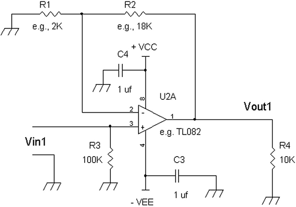
FIGURE 9.17 An example non-inverting amplifier with plus and minus power supplies.
The amplifier shown in Figure 9-17 is directly coupled to the input signal source, Vin1, and its output is directly coupled to a load resistor, R4. Load resistor R4 is just shown as an illustration and can be omitted. In essence this amplifier will amplify not only AC signals, but also DC signals.
Note that an input bias resistor, R3, is required so that even if the input signal Vin1 is disconnected, the op amp will be properly biased at the input terminal. Although R3 is shown as 100KΩ, it can be almost any value within reason. That is, it does not make sense to have R3 = 1Ω because that will load down the input signal source, Vin1, and drain excessive current, or worse, cause the input signal source to be damaged. Typical input bias resistances for R3 are in the range of 100Ω to 10KΩ when using op amps with bipolar input stages such as the NE5532 or LM741, etc. For op amps that have field effect transistor (FET, MOSFET, or JFET) input stages such as the TLC272, TL082, and OPA2134, the input bias resistor R3 can be as high as 10MΩ.
If in doubt, you can find a variety of field effect transistor input op amps by a web search or by searching your op amp at www.mouser.com or www.digikey.com and specifying an input bias current < 2 nA (< 0.002 μA or < 2000 pA) at the 25-degree Celsius/centigrade rating. For example, the TL082 has a maximum input bias current 200 pA rating at 25 degrees C.
A general rule of thumb is if the input bias current multiplied by the input resistance (R3) or the feedback resistor (R2) is less than 10 mV, then you are OK. For example, if we used an LM1458 op amp, with a worst case 500 nA input bias current, then we want 500 nA × R3 < 10 mV or R3 <10 mV/500 nA, R3 < 20KΩ. This is just a general rule of thumb, and if you are working in measuring or instrumentation circuits, then it may be best to choose a low offset voltage (Vos) field effect transistor op amp such as the OPA2134 or LF412.
For a non-inverting gain amplifier, the gain is:
Av = Vout1/Vin1 = (R1 + R2)/R1
For example, in the circuit, R1 = 2KΩ and R2 = 18KΩ:
Av = (R1 + R2)/R1 = (2KΩ + 18KΩ)/2KΩ = 20KΩ/2KΩ = 10
Av = 10
For non-inverting gain op amp circuits, the gain is Av = (R1 + R2)/R1 and the output resistance at Vout1 → 0Ω. That is, we normally do not have to worry about having the gain reduced if we load the output of the op amp with any range of resistance values as long as the op amp’s output stage can deliver sufficient current. But be aware that normally the output current limit is in the ± 10 mA range.
Now let’s intuitively understand how gain equation:
Av = Vout1/Vin1 = (R1 + R2)/R1 is derived. (See Figure 9-17.)
Recall the voltage at the (+) input terminal and the (–) input terminal is the same. In a negative feedback system, the (+) input terminal (e.g., U2A pin 3) determines the voltages at the output and (–) input terminal.
As a reminder note that you have to ensure that the (+) input always has a DC path to a voltage source. If you leave the (+) input unconnected or coupled to a capacitor, your circuit will not work. Now let’s go back to how this circuit works.
We see that R1 and R2 form a voltage divider for the output voltage, Vout1. That is: Vout1[R1/(R1 + R2)] = voltage at the (–) input terminal (e.g., U2A pin 2 in Figure 9-17). But we know that the (–) input terminal’s voltage = (+) input terminal’s volts, which is Vin1.
Therefore, Vout1[R1/(R1 + R2)] = Vin1, which leads to:
[Vout1/Vin1][R1/(R1 + R2)] = 1
and if we divide by [R1/(R1 + R2)] on both sides of the equation:
[Vout1/Vin1] = 1/[R1/(R1 + R2)] = (R1 + R2)/R1
Vout1/Vin1 = (R1 + R2)/R1
This confirms the previously stated gain equation for Av for a non-inverting gain amplifier. What’s happening inside the op amp is that it is providing a voltage at Vout1 such that when the voltage is attenuated via R1 and R2, the voltage at the (–) input terminal matches the voltage at the (+) input terminal, which is Vin1. This is how a negative feedback system works. So even if you try to load down the op amp by lowering the resistance of R4, the op amp will compensate to deliver a voltage at Vout1 that ensures that the voltage at the (–) input terminal matches the voltage at the (+) input terminal.
But also note that the op amp has output current limitations, and we have to be mindful how we set the gain of the amplifier while working within the output current capability of the op amp. The feedback resistors R1 and R2 also load the op amp at Vout1. For example, we will get into trouble if we set R1 = 2Ω and R2 = 18Ω. The op amp’s output terminal will see the (R1 + R2) as an “extra” load resistor, which will be 2Ω + 18Ω or 20Ω. If the op amp has a 10-mA maximum output current, then the maximum output voltage (e.g., at U2A pin1) will be ± 20Ω × 10 mA or ± 200 mV, which is a very limited output swing.
Often it is better to protect your input terminals from external DC bias voltages riding on top of AC signals. There are some devices that will provide an output signal with a DC bias voltage, which will cause a directly coupled amplifier such as in Figure 9-17 to overload. For example, if +VCC = +6 volts and –VEE = –6 volts and Vin1 = (1 volt DC + VAC_signal), and Av = 10, then:
Vout1 = 10 × Vin1
Vout1 = 10 × (1 volt DC + VAC_signal) or
Vout1 = 10 volts DC + 10 VAC_signal
However, since the power supplies are ± 6 volts, there is no way that the op amp U2A can provide 10 volts DC at Vout1. Therefore, the amplifier will be clipped to the positive rail at Vout1 and there will be no AC voltage at Vout1. We can fix this “problem” by AC coupling via an input capacitor. See Figure 9-18.
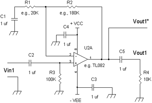
FIGURE 9.18 Using an input capacitor, C2, to block any DC voltage from Vin1 while passing AC signals.
By using an input coupling capacitor, C2, any DC bias voltage riding on top of the AC signal from Vin1 is eliminated at the (+) input terminal (e.g., U2A pin 3). Thus, the DC voltage at pin 3 is 0 volts, which leads pin 2, the (–) input, to have also 0 volts DC, and this further leads to the DC voltage at pin 1 is also 0 volts. Capacitor C1 at 1μf is used to provide an AC short circuit to ground such that the AC gain is still (R1 + R2)/R1 or 10 in this example with R1 = 20KΩ and R2 = 180KΩ. If you notice carefully, the resistors R1 and R2 have been scaled up tenfold from Figure 9-17. Why? The reason is if we want the same low-frequency response with R1 = 2KΩ and R2 = 18KΩ, C1 would have to be 10 μf. In practice, it is harder to find a 10 μf non-polarized capacitor when compared to obtaining a 1 μf capacitor.
Capacitor C1 also is used to prevent amplifying the op amp’s internal offset voltage, Vos, which is usually in the 5 mV to 10 mV range for general purpose amplifiers. If C1 were replaced with a 0Ω resistor, then we have a DC gain of 10, which will result in a DC voltage at the output of 10 × Vos. For example, if Vos = ± 10 mV, then the output DC voltage can be ± 10 × 10 mV or ± 100 mV DC. With C1, the offset voltage is just voltage “followed” and the DC gain with C1 is 1. So, with C1 installed, Vout1’s DC voltage is just Vos or typically ≤ 10 mV DC.
Note that the built-in offset voltage in the op amp can be a positive or negative DC voltage. An ideal op amp will have Vos = 0 volt. You can buy precision op amps with Vos ≤ 1.0 mV such as the LF412A (note the LF412A has a tighter Vos specification ≤ 1.0 mV than the LF412 without the “A” designation, which has Vos ≤ 3.0 mV).
Figure 9-18 also shows that you can AC couple the output signal via C5 with Vout1 or have the output signal DC coupled via Vout1". An AC coupled output is useful for blocking any DC voltage that may go into the output terminal of U2A. This is important in some cases where the output terminal of an amplifier is driving another circuit that has a DC bias voltage. If you use the Vout1" terminal, the DC bias voltage from the other circuit will be “shorted” DC wise to ground or zero volts that may cause this other circuit to have the wrong DC bias and not operate correctly. Thus, to play it safe, use a DC blocking output capacitor, C5, and also remove the load resistor R4.
If you are using a single power supply non-inverting amplifier, see Figure 9-19.
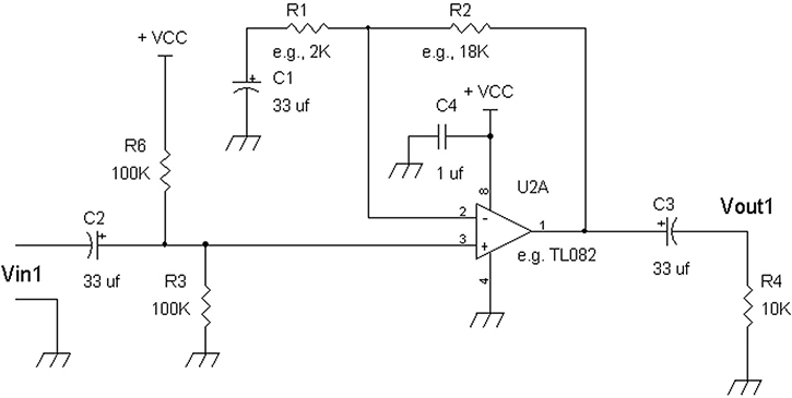
FIGURE 9.19 A single power supply non-inverting gain amplifier.
The AC gain of this amplifier is again Av = (R1 + R2)/R1. To maximize on voltage swing, the DC bias voltage at the (+) input is set at +VCC/2. For example, if +VCC = 9 volts, the DC bias voltage is set to 4.5 volts at pin 3 of U2A via voltage divider R3 and R6, where R3 = R6. The AC input resistance is R3 || R6, which is 100KΩ || 100KΩ or 50KΩ. Note that resistor R6 is connected to +VCC, which is an AC ground.
Because we are using a single supply, we can use polarized electrolytic capacitors (C1, C2, and C3) that allow for higher capacitance values at low cost.
To analyze this circuit DC-wise, see Figure 9-20 where we remove the capacitors C1, C2, and C3. Since these capacitors block DC currents when charged to their final value, they are open circuits in terms of DC analysis.

FIGURE 9.20 Removing C1, C2, and C3 simplifies the circuit for DC analysis.
By removing the capacitors, a simplified circuit is shown in Figure 9-20 on the right. On the left side circuit, since R1 and R4 are disconnected on one end, they can be removed, which is shown on the right side circuit.
Here we see only a voltage divider circuit with R3 and R6, along with R2, the feedback resistor. However, because the op amp’s (–) input terminal has a high input resistance, there is no current flowing through R2. This implies there is no voltage across R2 since the voltage across R2 is equal to VR2 = I2 × R2, where I2 = current flowing into the (–) input terminal. Since I2 = 0 amp flowing into the (–) input:
VR2 = 0 amp × R2 = 0 volt
Therefore, we can simplify further this right side circuit. See Figure 9-21.
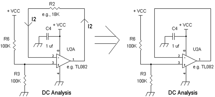
FIGURE 9.21 With zero current I2 flowing through feedback resistor R2, the circuit reduces to a simple voltage follower amplifier for DC analysis.
Because there is 0 volts across R2, this means the voltage at output pin 1 is the same voltage at pin 2, the (–) input. This then means we can replace R2 with 0Ω or a wire since we will get the same result, the voltage at pin 1 is the same as the voltage at pin 2. Thus, the DC voltage at pin1 is just +VCC/2 since the voltage at the (+) input pin 3 is the same as the voltage at (–) input pin 2 when negative feedback is applied.
Figure 9-22 shows a model of a non-inverting gain amplifier for AC signals.
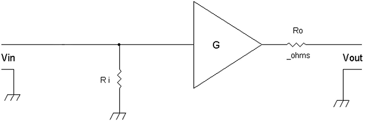
FIGURE 9.22 A generalized model for the non-inverting amplifiers, with G = Av.
From Figure 9-22 we have:
Ro ~ 0Ω
NOTE: Keep in mind that op amps generally deliver about ± 10 mA into a load.
Ri = R3 in Figures 9-17 and 9-18, Ri = R3 || R6 in Figures 9-19 and 9-20. Typically, Ri ≥ 10KΩ.
G = Av = [(R1 + R2)/R1] for Figures 9-17, 9-18, 9-19, and 9-20.
Also, be sure to choose resistance values for the feedback network R1 and R2 such that it does not load the op amp’s output current excessively. Determine the maximum signal output and divide by (R1 + R2) to determine the current draw from the op amp. Generally, this current draw should be less than 50 percent of the op amp’s maximum output current.
For example, in Figure 9-7, if the maximum current output is 10 mA and you are using ± 12 supplies, for Av = 5 you can use R2 = 4020Ω and R1 = 1000Ω. Note Vsupply = 12 volts.
Worst case, the load current due to the feedback network will be:
Vsupply/(R1 + R2)
For this example, it will be 12 volts/5020Ω. This translates to about 2.4 mA, which is less than the 10-mA output limit. So, this is OK.
On the other hand if you choose R2 = 120Ω and R1 = 30Ω, the current draw will “want to be” 12 volts/(120Ω + 30Ω) = 80 mA.
This will cause the amplifier to clip at the output, and the waveform will clip at Voutput max ≤ (R1 + R2) × 10 mA or ≤ 150Ω × 10 mA or ≤ 1.5 volts peak.
If a non-inverting gain amplifier circuit is generally set for a gain or Av ≥ 2 with an op amp that has rail to rail output voltage but does not have rail to rail performance at the input terminal, then this circuit can deliver rail to rail at the output while keeping within the input voltage range for proper operation. The reason is that by having a gain of ≥ 2, the input voltage range no longer has to go from rail to rail, but instead ≤ 50 percent of the output voltage range. For example, suppose a single supply amplifier shown in Figure 9-17 has an input range of +VCC – 1.2 volts to –VEE, and the power supplies are +VCC = +2.5 volts and –2.5 volts. This means the input terminal must be in the range of –2.5 volts to (+2.5 volts – 1.2 volts), which is between –2.5 volts to +1.3 volts. Now suppose the gain is +2 by having R1 = R2 = 10KΩ. At the zero-signal condition, the output voltage is 0 volts.
If the input signal is between –1.25 volts and +1.25 volts (e.g., a sine wave input signal whose peak amplitude is 1.25 volts), then the output will be twice that due to setting Av = 2. Therefore, the output voltage will swing from –2.5 volts to +2.5 volts. And note that the input voltage signal range of –1.25 volts and +1.25 volts is within the input range of the op amp at –2.5 volts to +1.3 volts.
Troubleshooting Non-Inverting Op Amp Circuits via an Oscilloscope, Signal Generator, and DVM
Here are some tips on basic debugging techniques:
1. Make sure that the power supply terminals are connected correctly and use a voltmeter to confirm proper power supply voltages at the power pins. Be sure to have the op amp’s data or spec sheet handy.
2. Make sure there is at least a ≥ 0.1 μf decoupling capacitor wired or soldered closely to each power pin (e.g., plus supply pin 8 and negative supply pin 4 of an LM1458) and ground. For example, see the 1 μf power supply decoupling capacitors C4 and C3 in Figure 9-17. For a single supply circuit, you need only one decoupling capacitor since the other power pin is usually grounded. See Figure 9-19 where positive supply pin 8 of U2A is decoupled with 1 μf capacitor C4 to ground, while its negative power pin 4 is connected to ground. Without power supply decoupling capacitors, op amps can oscillate or give noisy output signals on their own.
3. Confirm that the input DC voltages are within the range as specified by the data sheet. For example, an LM358 at +5 volts power supply has an input voltage range from about 0 volts to 3.5 volts. Use a voltmeter to confirm that the non-inverting input terminal (e.g., pin 3 or 5 in an LM358) is within the input voltage range.
4. Measure the voltage with a DVM across the non-inverting input pin and the inverting input pin of the op amp. Confirm that the voltage is ~ 0 volt. If the voltage is not zero such as 0.5 volts DC, then the op amp circuit is not operating properly.
5. For op amp circuits with positive and negative supplies, verify that the DC output voltage is close to zero. Verify that the non-inverting input terminal is connected via a wire or resistor (or a coil) to a DC potential such as ground or a bias voltage. With an ohm meter (DVM) and with the power supplies turned off, confirm that there is some resistance from the non-inverting input terminal to ground to a DC voltage line. For example, in Figure 9-18, the non-inverting input pin 3 is connected to ground via a 100K ohm resistor (R3) to establish a 0-volt DC bias.
6. For op amp circuits with positive and negative supplies, if you are getting unexpected DC voltages at the output pin, then with the input signal source disconnected, try temporarily connecting the non-inverting input terminal to ground via a resistor (e.g., 10KΩ or lower) and re-measure the DC output voltage. If it is now correct, look for a bad bias resistor or bad connection in the non-inverting input terminal area. If connecting the non-inverting input terminal to ground does not help, then temporarily connect a wire or low-value resistor (e.g., 100Ω) from the output to inverting input terminal to form a voltage follower. If you now get a DC voltage ~ 0 volts, then recheck the feedback resistor network for the correct values. But it may be easier to just use a DVM and measure the resistance of the feedback network (e.g., R1 and R2 in Figure 9-7) with the power turned off.
7. If after #1 to #6, you are not getting anywhere, replace the op amp, but make sure the original op amp could operate at the power supply voltages. For example, if the power supply provides ± 12 volts DC and the circuit does not seem to work, verify that the op amp is not a lower voltage version such as an LMV358 (e.g., +5.5 volts maximum) or a TLC272 where a supply voltage of more than ± 8 volts will cause damage.
8. If the DC bias conditions are correct, but the AC signals are distorted or do not have correct amplitudes given the gain setting [(R1 + R2)/R1], then first check the resistance values of the feedback resistors. Also make sure the feedback network resistance value of (R1 + R2) ≥ 500Ω is not low enough to cause current limiting at the output that will cause clipped waveforms.
9. If the low-frequency (e.g., 20 Hz) response is poor—such as less than 50 percent of amplitude when compared to the signal amplitude at a mid-band frequency (e.g., 1000 Hz)—check the input and output coupling capacitors. If they measure correctly, check the frequency response at the non-inverting input pin (e.g., pin 3 or 5 in a dual op amp). If that’s OK, check the frequency response at the output pin of the op amp such as pin 1 or 7 of a dual op amp. If there is a loss in low-frequency response, see if there is an AC coupling capacitor in the feedback network, such as C1 in Figure 9-18 or C1 in Figure 9-19. If you suspect there is a problem like the capacitance is not high enough, parallel a larger capacitance across C1, such as 2.2 μf capacitor. If the capacitor is ceramic, check the maximum working voltage. For example, if you use a 1-μf, 6.3-volt capacitor and the DC voltage across it is +5 volts, chances are that the true capacitance will be half of that, or 0.5 μf, which will cause a poorer low-frequency response.
10. Also, if electrolytic capacitors are used, measure with a volt meter (DVM) that the DC voltage across the capacitor matches the polarity markings of the capacitor. If you measure a reverse bias voltage across an electrolytic capacitor, turn off the power immediately, replace the capacitor and install a new capacitor with the correct polarity.
11. Another troubleshooting technique is to confirm that the feedback decoupling capacitor is an AC short circuit. Apply a sine wave signal between 200 Hz and 500 Hz at the input and measure the AC voltage across the C1/R1 junction (e.g., of Figure 9-19). There should be a very small AC voltage there when compared to the AC signal at the non-inverting input pin (e.g., pin 3 or 5 in a dual op amp).
12. Also check if the circuit was for a dual op amp but a single op amp was installed instead, or vice versa. Both single and dual op amps have 8 pins total and some pins are common, such as the –V supply pin 4, non-inverting input pin 3, and inverting input pin 2; however, the other pins 1, 5, 6, 7, and 8 are not the same for a single op amp and dual op amp.
This concludes an introduction to non-inverting gain op amp circuits. Next, let’s take a look at inverting gain amplifiers.
Inverting Gain Amplifiers
We now turn to inverting gain op amp circuits where they produce an inverted waveform at the output when compared to the input signal. See Figure 9-23.

FIGURE 9.23 An inverting gain op amp circuit with plus and minus power supplies.
The gain Av = Vout1/Vin1 = –R2/R1. So, if we keep the same feedback resistors as in the circuit of Figure 9-17, that is, R1 = 2KΩ and R2 = 18KΩ, we find that Av = –18K/2K or Av = –9. Note the magnitude of the gain for the inverting amplifier: –R2/R1 is different from the non-inverting gain amplifier’s formula of (R1 + R2)/R1 = 1 + R2/R1. The difference between the magnitudes of the two gains of non-inverting amplifier and inverting amplifier is just 1. For example, the non-inverting gain amplifier will have a gain of 10 with R1 = 20KΩ and R2 = 180KΩ, while the inverting gain amplifier will have a gain of –9.
The input resistance is just R1. So why is this? The non-inverting input is connected to ground; its voltage is 0 volts or Vi (+) = 0 volts. Since in a negative feedback amplifier the voltage at the inverting input terminal is the “same” as the voltage in the non-inverting input terminal, we can deduce that the voltage at the inverting input terminal Vi (–) is also 0 volts. Thus, R1 on the right side connection to pin 2 of U1A is “virtually grounded.” Therefore, referenced to ground, the input resistance is R1. In other words, if we look at an equivalent resistor referenced to ground from the inverting input node Vi (–), its resistance is Rsc, where Rsc is a short circuit to ground, equivalently. Rsc is a very low equivalent resistor because there is a large magnitude open loop gain inside the op amp. It is very similar to the feedback resistor in a one-transistor amplifier from Chapter 8 where we found that with a high-gain amplifier the input resistance looking into the base with the collector-to-base resistor is very low.
Because of R2, the feedback resistor, Rsc = R2/(1 + a), where “a” is the open loop gain. For example, if we have an NE5532 amplifier whose open loop gain is ~ 20,000 at 2 kHz, then the Rsc = R2/(1 + 20,000) ~ R2/20,000. Thus, if R2 = 180KΩ, Rsc ~ 180KΩ/20,000 or Rsc ~ 9Ω.
Since R1 = 20KΩ and Rsc = 9Ω << 20KΩ, the 9Ω Rsc resistor equivalently shorts to ground the right side lead of R1 at Vi (–).
In terms of the output resistance at Vout1, the op amp with the negative feedback resistor R2 has an output resistance close to zero ohms. The amplifier in Figure 9-23 amplifies DC and AC voltages at Vin1. For example, if Vin1 = 1.0 v DC, then Vout1 = –(R2/R1) + 1 volt DC. For example, if R2 = 180KΩ and R1 = 20KΩ, the output voltage will be: Vout1 = –(180K/20K) × 1 volt DC or Vout = –9 volts DC. Note that the supply voltage should be at least a few volts higher than 9 volts, such as ± 12-volt supplies for +VCC and – VEE.
To amplify only AC signals, use AC coupling capacitors C1 for the input, and C5 for the output (see Figure 9-24). Alternatively, you can directly couple your output signal via Vout1". Note the low frequency cut-off is fc = 1/(2πR1C1) at the input when driven by the low source resistance, Rs, signal such that Rs << R1. For example, many generators have 50Ω source resistances that are << R1 = 20KΩ. For output Vout1, the cut-off frequency is fc = 1/(2πR4C5).

FIGURE 9.24 An inverting gain op amp circuit with AC signal coupling capacitors C1 and C5. Input resistance ~ R1 when C1 is an AC short circuit.
NOTE: Because the inverting gain op amp circuit has the (+) input tied to a fixed DC voltage within its common mode voltage range, rail to rail output is achieved with any op amp specified with rail to rail output. That is the input range of the op amp does not have to include rail to rail performance. (See Figure 9-24.)
Note that Figures 9-24 and 9-25 look similar with the input resistors R1 and R1" with R2 and R_BC. The difference is the op amp U1A has very high gain via many transistors inside, and a very low output resistance compared to the amplifier in Figure 9-25.

FIGURE 9.25 A one-transistor amplifier from Chapter 8 that resembles an inverting gain op amp circuit for small voltage gains Av ~ –R_BC/R1", where R_BC is the feedback resistor. Input resistance ~ R1” when C1 is an AC short circuit.
One can think of Figure 9-25 as simplified inverting gain amplifier. It does have one or two advantages over an op amp. For one advantage, even with typical transistors such as the 2N3904, it can deliver very wide bandwidth. For example, if you want to make a cheap inverting gain of –2 amplifier at 1.5 volts supply, you can set RL = 470Ω, R_BC = 2KΩ and R1" = 1KΩ. The –3 dB bandwidth will be in the order of 5 MHz.
For another advantage, not too many inexpensive op amps work at +1.5 volts supply and have a bandwidth of about 5 MHz for a gain of –2.
In Figure 9-25 the amplifier’s gain is: Vout/Vin ~ –R_BC/R1" where R_BC/R1" < 3. However, this simple one-transistor amplifier cannot drive low-resistance loads, and will lose performance in terms of output swing. Also, the maximum gain from this amplifier is less than 3 for distortion less than 1 percent.
But for the flexibility to provide large voltage gain, low distortion, and the ability to load into low-resistance loads with minimal board space area, op amps are the way to go. They are available in even smaller packages such as surface mount versions. These can include SO-8 or SO-14 dual inline surface mount packages, but op amps are also available in even smaller sizes, such as a single amplifier in about the size of an SOT-23 transistor with five leads (e.g., two for power, two for inputs, and 1 for output).
Now let’s take a look at single supply inverting gain op amp circuits. See Figure 9-26.
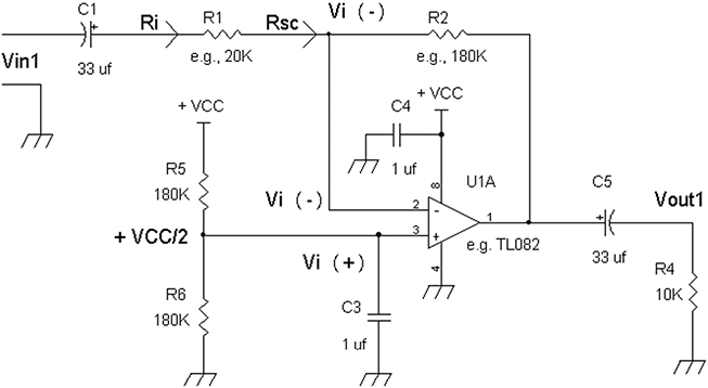
FIGURE 9.26 An inverting amplifier op amp circuit with a single power supply.
We want to maximize voltage swing by setting the output DC voltage to one-half the supply voltage. This is done by defining a DC voltage at the non-inverting input terminal (e.g., pin 3 for one section of a dual op amp). By negative feedback the voltages at the (–) and (+) input terminals pins 2 and 3 are equal, so Vi (+) = Vi (–) = +VCC/2. Also note that there is a voltage reference filter capacitor C3 that removes noise from +VCC such as power supply ripple. If there is power supply noise embedded into the +VCC/2 voltage it will be amplified by a factor of [1 + (R2/R1)]. In this example where R1 = 20KΩ and R2 = 180KΩ, and without C3 any noise from +VCC/2 will be amplified by [1 + (180K/20K)] or 10. Thus we want to filter any noise of power line frequency ripple signal that may be present in +VCC. In general, a roll-off frequency < 20 Hz is a good start. This is because C3 with R5 and R6 form a low-pass filter.
In Figure 9-26, the low-pass filter roll-off frequency is 1/[2π(R5 || R6) C3] which is: 1/[2π(180KΩ || 180KΩ) 1 μf] or 1/[2π (90KΩ × 1 μf)] = 1.77 Hz, which is less than 20 Hz. This means that for any ripple voltage or noise whose frequency is above 1.77 Hz, attenuation will occur. If you need more filtering to remove noise from +VCC, you can increase C3’s capacitance by using an electrolytic capacitor with its (–) terminal connected to ground. For example, a 33 μf 25-volt capacitor will reduce the noise about 33 times more when compared with the 1 μf for C3.
Since no DC currents flow into R1, and no DC current flows into R2, the DC voltage at output pin 1 is +VCC/2. See Figures 9-27 and 9-28. Also, if you look carefully in terms of DC analysis, Figure 9-26 resembles the non-inverting gain amplifier in Figure 9-19.
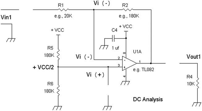
FIGURE 9.27 Capacitors C1, C3, and C5 are removed for DC analysis.
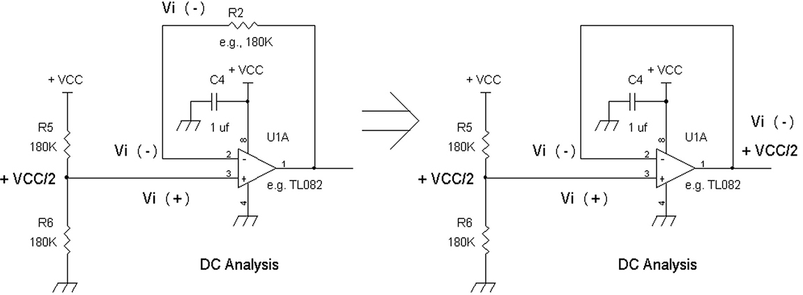
FIGURE 9.28 With R1 and R4 removed the circuit is simplified for DC analysis.
By removing the capacitors, we see on Figure 9-28 that the circuit is simplified for DC analysis and unconnected components such as R1 and R4 are removed.
Further simplification can be done as shown on the right side drawing of Figure 9-28 where R2 is replaced with a wire such that there is no current flowing through R2, which results in no voltage across R2. And, of course, a wire or 0Ω resistor has no voltage across it. Thus, as we can see on the schematic on Figure 9-28’s right hand side, all we are left with is a voltage follower with +VCC/2 into the (+) input of the op amp that results in +VCC/2 at the output pin 1 of U1A.
As a reminder when using a single supply, make sure you have sufficient voltage at the power pin. If you are using general purpose op amps such as LM741, LM4558, TL082, or higher performance ones like the NE5532 or LM4562, usually you can get by with a +VCC range of 9 volts ≤ +VCC ≤ 28 volts. However, should you decide to use lower-voltage op amps, most will work at +5 volts, but be aware that some of these low-voltage op amps have maximum supply voltages of +5.5 volts (e.g., LMV358) and of +12 volts (e.g., TL972 low-noise op amp has rail to rail output voltage).
We can model an inverting gain op amp circuit for AC input and output signals as shown in Figure 9-29.

FIGURE 9.29 A general model for an inverting gain amplifier.
For an inverting gain amplifier the AC gain G = Av = –R2/R1 and the AC input resistance Ri = R1, with R1 and R2 shown in Figures 9-23, 9-24, and 9-26. In all cases the AC output resistance, Ro ~ 0Ω for the inverting gain op amp circuits.
Troubleshooting Inverting Op Amp Circuits via an Oscilloscope, Signal Generator, and DVM
Here are some tips on basic debugging techniques for inverting gain op amp circuits, which are similar to the non-inverting gain circuits:
1. Make sure the power supply terminals are connected correctly and use a voltmeter to confirm proper power supply voltages at the power pins. Be sure to have the op amp’s data or spec sheet handy.
2. Make sure there is at least a ≥ 0.1 μf decoupling capacitor wired or soldered closely to each power pin (e.g., plus supply pin 8 and negative supply pin 4 of an LM1458) and ground. For example, see the 1 μf power supply decoupling capacitors C4 and C3 in Figure 9-23. For a single supply circuit you need only one decoupling capacitor since the other power pin is usually grounded. Without power supply decoupling capacitors, the op amps can oscillate or give noisy output signals on their own.
3. Measure the voltage with only a DVM across the non-inverting input pin and the inverting input pin of the op amp. Confirm that the voltage is ~ 0 volt. If the voltage is not zero across the two input terminals such as 0.5 volts DC, then the op amp is NOT operating properly.
NOTE: Do not try measuring the voltage across the input pins (e.g., pins 3 and 2 of a dual op amp) with an oscilloscope. You can short out one of the input pins. The ground lead of the oscilloscope probe or wire must always be connected to the ground connection of the circuit. In general, by an indirect connection, the ground lead of an oscilloscope is at ground potential. That is, the ground lead from an oscilloscope is not “floating” like the negative (and positive) lead of a DVM.
4. For op amp circuits with positive and negative supplies, verify that the DC output at the op amp voltage is close to zero. If it is not, verify that the non-inverting input terminal is connected to a DC potential such as ground.
5. If after #1 to #4, you are not getting anywhere, replace the op amp, but make sure the original op amp could operate at the power supply voltages. For example, if the power supply provides ± 12 volts DC and the circuit does not seem to work, verify that op amp is not a lower-voltage version, such as an LMV358 (e.g., +5.5 volts maximum) or a TLC272, where a supply voltage of more than ± 8 volts will cause damage.
6. If the DC bias conditions are correct, but the AC signals are distorted or do not have correct amplitudes given the gain setting [–R2/R1], then first check the resistance values of the feedback resistors. Also make sure the feedback network resistance value of R2 ≥ 500Ω is not low enough to cause current limiting at the output that will cause clipped waveforms.
7. If the low-frequency (e.g., 20 Hz) response is poor, such as less than 50 percent of amplitude when compared to the signal amplitude at a mid-band frequency (e.g., 1000 Hz), check the input and output coupling capacitors. If they are OK, check the frequency response at the output pin of the op amp such as pin 1 or 7 of a dual op amp. If there is a loss in low-frequency response, see if there is an AC coupling capacitor at the input, such as C1 in Figure 9-24 or C1 in Figure 9-26. If you suspect there is a problem like the capacitance is not high enough, parallel a larger capacitance across C1, such as a 2.2-μf capacitor. If the capacitor is ceramic, check the maximum working voltage. For example, if you use a 1-μf 6.3-volt capacitor and the DC voltage across it is +5 volts, chances are that the true capacitance will be half of that, or 0.5 μf, which will cause a poorer low-frequency response.
8. Also, if electrolytic capacitors are used, measure with a voltage meter that the voltage across the capacitor is correct with the polarity markings of the capacitor. If you measure a reverse bias voltage across an electrolytic capacitor, turn off the power immediately, replace the capacitor, and install a new capacitor with the correct polarity.
9. Check to make sure the phase at the output is inverted relative to the phase of the input signal. If you are getting the same phase signal at input and output, then the op amp may be damaged or open circuited from the feedback and input resistors (e.g., R2 and R1). As a result of the op amp being open circuited, the signal will travel through R1, then to R2 to the output. If you have no power to the op amp, a feed-through condition will also occur and the signal from R1 to R2 may travel through and there will be no inversion of the input signal at the output terminal.
A telltale sign that something is wrong is if you probe the inverting input of the op amp (e.g., pin 2 or pin 6 of a dual op amp) and see a signal, then something is wrong because you should see no signal at all. This is because the inverting input in an inverting gain amplifier is a virtual ground, or a virtual AC ground (e.g., in a single supply circuit).
10. Also check if the circuit was for a dual op amp but a single op amp was installed instead, and vice versa. Both single and dual op amps have 8 pins total and some pins are common, such as the –V supply pin 4, non-inverting input pin 3, and inverting input pin 2; however, the other pins 1, 5, 6, 7, and 8 are not the same for a single op amp and dual op amp.
11. In an inverting gain amplifier you cannot make the feedback resistor R2 = 0Ω, since this will result in a zero output. Also, making the feedback resistor (e.g., R2) low resistance (e.g., < 500Ω) can cause the op amp’s output waveform to distort due to current limiting. Recall that the feedback resistor is also connected to the inverting input terminal, which is a virtual ground. So, the feedback resistor is a “direct” load resistor to the output terminal.
Brief Notes on Both Non-inverting and Inverting Gain Amplifier Circuits
• If you are providing signals to the outside world, such as to a connector that will later be used with a cable or wire, please add a 47Ω series resistor between the output of the op amp and the connector. Or if you are driving any shielded cable or coaxial cable with the op amp, also add a series resistor between the output of the op amp and the cable. The reason for adding a series resistor is to prevent the op amp from oscillating, and to provide some short circuit protection. This is especially true when a person can inadvertently short out a connector while trying to connect a cable to it.
• For both types of amplifier circuits, choose an op amp that is “unity gain compensated.” This will ensure that there will be no parasitic oscillations. Most op amps are unity gain compensated such as the ones listed in this chapter.
• The high-frequency bandwidth is determined by the op amp’s unity gain bandwidth divided by [1 + (R2/R1)]. Usually, there is a typical or minimum unity gain bandwidth specification on the data sheet. For example, if you are using a TLO82 op amp that has about a 3-MHz unity gain bandwidth, the high-frequency bandwidth of either inverting or non-inverting amplifiers is determined by the ratio of R2 over R1. In a previous example R1 = 2KΩ and R2 = 18KΩ. Therefore, with a TL082 the high-frequency bandwidth is 3 MHz/[1 + (18KΩ/2KΩ)] = 3 MHz/10 or 300 kHz. This 300-kHz bandwidth is for a non-inverting gain of +10 or an inverting gain of –9.
• The op amps also have a power bandwidth specification or slew rate specification. Generally, for instrumentation such as monitoring slow changing DC voltages, a slew rate of ≥ 0.2 volts per microsecond will work. For audio circuits with ≤ 5 volts peak to peak output, ≥ 0.5 volts per microsecond is fine. But for a large audio signal voltage output of ~ 24 volts peak to peak, ≥ 1 volt per microsecond will do. Once you have to work with signals beyond 20 kHz, it’s best to find an op amp ≥ 20 volts per microsecond. For example, for even standard resolution TV (SDTV) analog signals such as 480i, you will need ≥ 50 volts per microsecond with a high-frequency bandwidth ≥ 5 MHz.
• Op amps with negative feedback, such the non-inverting and inverting amplifiers, have power supply noise rejection at their power pins. This means if there is a power supply ripple from a raw supply, the op amp will keep the ripple from showing up at the output. However, it is usually better to use a voltage regulator for powering op amps. See the next section in this chapter.
A Short Look at Linear Voltage Regulators
Voltage regulators provide a constant voltage to an electronic circuit, even though the raw power supply is varying in DC voltages. For linear voltage regulators to operate correctly, the incoming voltage must be larger than the regulated voltage at the output. For example, if you have a power supply that varies between 9 volts and 12 volts due to power supply ripple or changes in the AC power line voltage, you can provide a regulated +6 volts or +5 volts via an LM7806 or LM7805 three-terminal regulator. If you want to adjust to different regulated voltage, you can use an LM317T integrated circuit and two resistors to set the voltage, which will be greater than two volts difference between the incoming voltage and the regulated output voltage.
Another reason for using linear voltage regulators is to remove high-frequency noise from switching power supplies. For example, an efficient wall power supply may have switching noise in the 1-MHz region added to its regulated DC voltage. A voltage regulator can remove the switching noise.
Voltage regulators are available in through-hole and surface mount packages. We will be looking at through-hole versions, which are easier to use for DIY projects, plus they can be mounted onto heat sinks.
Types of Linear Regulators Starting with “Standard” Fixed Voltage Versions
What is a voltage regulator? It is a device that takes in an incoming raw DC voltage and provides a constant lower voltage. The incoming raw DC voltage may vary in DC amplitude with noise or ripple voltages riding on top of a DC voltage. The voltage regulator then removes the noise or ripple voltages and provides a lower constant voltage.
For example, if the incoming DC voltage has a range of +7 volts to +10 volts, that is, a minimum of +7 volts and a maximum of +10 volts, and this incoming DC voltage is connected to a +5 volt regulator, the output of the regulator will be a constant +5 volts.
A voltage regulator requires a DC input voltage that does not dip below its minimum input voltage rating. This means that the DC input voltage must not be a pulsating DC voltage such as a rectified AC voltage without a filter capacitor, which means the DC voltage can dip to 0 volts. If such an instance happens, the regulator will just pass through the input voltage that includes the pulsations. Figure 9-30 shows an example of a pulsating DC voltage waveform.
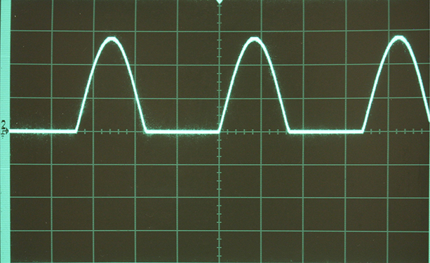
FIGURE 9.30 A half wave rectified voltage without a filter capacitor that is NOT the type of DC input voltage required for a voltage regulator.
The waveform at times goes to 0 volts or ground. Instead, see Figure 9-31, a half wave rectified voltage with a filter capacitor that is more suitable for use with a voltage regulator.
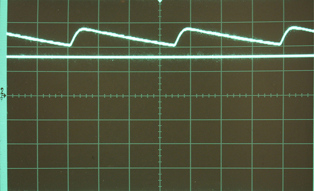
FIGURE 9.31 Top trace: A half wave rectified voltage that provides a DC voltage with a “saw-tooth” ripple voltage riding on top of the average DC voltage for the input voltage into a voltage regulator. Bottom trace: Regulated voltage output. The center horizontal line is at 0 volts.
Note the wave does not go to ground and has a minimum DC voltage at the lowest point of the sawtooth. This lowest point voltage must be equal to or greater than the “drop-out” voltage specification of the voltage regulator. For example, if Figure 9-31 is at 2 volts per division, the DC voltage has a minimum voltage of about +4 volts and a maximum voltage of about 2.8 div × 2 volts/div, or about 5.6 volts peak. If a standard voltage 3.3-volt voltage regulator is used, generally, the drop-out voltage is about 2 volts to be on the safe side, which would mean a minimum input voltage = 3.3 volts + Vdrop-out is needed. This would be 3.3 v + 2 v = 5.3 volts, which would mean when the waveform dips below 5.3 volts, the voltage regulator will stop working properly since the example has the waveform at a peak of 5.6 volts only briefly and dipping to down 4.0 volts. To “fix” this, you can use a low–drop-out regulator that usually has a drop-out voltage of about 0.5 volts. This means the minimum input voltage = 3.3 volts + 0.5 volt or 3.8 volts. Since the example waveform has the minimum voltage at 4.0 volts, the low–drop-out voltage regulator will work properly, but just barely.
Drop-Out Voltage Summary
Again, most standard linear voltage regulators (e.g., with fixed and adjustable regulated output voltages) require that the “dip” or minimum of the DC input voltage is at least 2 volts above the regulated output voltage. The drop-out voltage is specified as the minimum voltage between the input and output of the regulator to ensure that voltage regulation takes place. In the example of having 2 volts above the regulated voltage, the drop-out voltage is 2 volts.
However, there are low–drop-out voltage linear voltage regulators that can regulate the voltage when the “dip” or minimum of the DC input voltage is at least 0.50 volt above the regulated output voltage. In this case, the drop-out voltage is 0.5 volts, which when compared to the 2-volt drop output voltage for standard voltage regulators, we can see why the term “low–drop-out voltage” is used.
Voltage Selections, Packages, Pin Outs and Schematics
For standard fixed-voltage output regulators in TO-220 (1 amp) and TO-92 (100 mA) packages, see Figure 9-32. Notice that the pin outs are not the same for positive and negative voltage regulators.
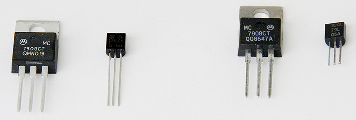
FIGURE 9.32 Fixed-output voltage regulators shown with 1 amp TO-220 and their mounting tabs, and the smaller 100 mA TO-92 packages that look like transistors (e.g., 2N3904), but they are actually integrated circuits.
This is important to notice that in a positive regulator, reading from the side where the part number is printed, the sequence is input, ground, and output, whereas in a negative voltage regulator, the first two terminals are reversed have the sequence, ground, input, and output. For TO-220 packages, the metal tab is always connected to the middle terminal. That is in a TO-220 fixed-voltage regulator, the metal (mounting) tab is ground for a positive version, while for a negative fixed-voltage regulator the tab is the input voltage terminal. It is very important to never ground the negative voltage regulator’s tab, or you will short out the raw input DC supply.
If you are using a low-power TO-92 linear voltage regulator, such as the positive voltage 78Lxx or negative voltage type 79Lxx, be aware of the pin out because they are different. Again, from the flat side where you are reading the part number, the sequence for the positive TO-92 package is output, ground, and input, which is a reverse sequence from its bigger TO-220 version. For the negative voltage regulator in TO-92 package, the pin out sequence as read from the flat side is ground, input, and output, which is the same as its TO-220 higher current version. Keeping track of all these packages in your head can be confusing. If in doubt, look up the data sheet.
See a schematic diagram for fixed-output voltage regulators in Figure 9-33 and their associated decoupling capacitors.
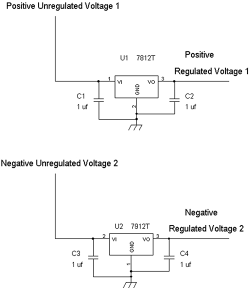
FIGURE 9.33 Schematic diagrams for standard positive and negative voltage TO-220 regulators with decoupling capacitors C1, C2, C3, and C4. Notice that the first two pins U1 are reversed from the pins in U2 (Vi and Gnd).
Knowing the Pin Out Sequence Is Important
See Figure 9-34 for the pin out sequence for both TO-220 and TO-92 fixed (e.g., not adjustable) voltage regulators.
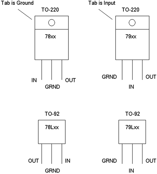
FIGURE 9.34 Pin out sequences as read from the front side of the voltage regulators that have their printed markings. The TO-92 illustrations are drawn larger for clarity of pin outs. See Figure 9-32 for a comparison of the real sizes of the different packages. (7800 series = Positive regulator, 7900 series = Negative regulator).
Common fixed output voltages include +3.3 volts (78Mxx for 500 mA or 78Lxx for 100 mA), with 78xx (positive) for 1 amp at +5 volts, +6 volts, +8 volts, +10 volts, +12 volts, +15 volts, +18 volts, and +24 volts. In the 78xx part number, you replace the “xx” with the voltage you require. For example, if you need a +12-volt regulator 78xx → 7812, or if you need a +5-volt regulator, the correct part number is 7805.
Equivalently, there are LM340 series regulators equivalent to the 78xx series. Here, the numbering system requires a dash such as a +5-volt regulator is named as LM340-5. Voltage selection on the LM340 series is the same for the 78xx series when using parts made by Texas Instruments (TI).
For negative voltage regulators, the 79xx series can output regulated negative voltages of –5 volts, –6 volts, –12 volts, –15 volts, –18 volts, and –24 volts. Again, as an example, if you need a –6-volt regulator, the part number will be 7906.
NOTE: The raw input DC volts should not exceed any voltage higher than 30 volts at its peak for positive voltage regulators (78xx) and no lower than – 30 volts peak for negative voltage regulators (79xx); otherwise, they can be damaged.
Low–Drop-Out Voltage Regulators
There are low–drop-out (LDO) voltage regulators that require that the input voltage is only ≥ 0.5 volt above the regulated output voltage. Again, this means the drop-out voltage is 0.5 volt. Also, these LDO regulators have the same pin out sequence as the previously mentioned standard fixed regulators. That is, the pin outs for the low–drop-out positive voltage regulator LM2941-x are the same as the LM78xx TO-220 regulators. The low–drop-out negative voltage regulator, LM2990-xx, will have the same pin out for the LM79xx TO-220 packages. See Figure 9-35.
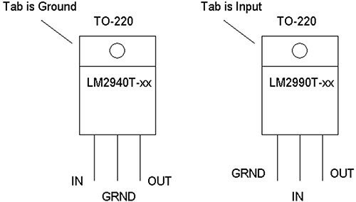
FIGURE 9.35 Low–drop-out voltage regulators and their pin outs. (LM2940 series = Positive regulator, LM2990 series = Negative regulator).
However, there are a couple of noteworthy differences between the low–drop-out regulators compared to the standard ones.
• The maximum positive input voltage is +25 volts for the LDO regulators versus +35 volts absolute maximum for the standard versions (LM78xx).
• The decoupling capacitors have to be larger for the output capacitors in low–drop-out regulators. Typically, you can use electrolytic capacitors of 33 μf at 35 volts for both the input and output decoupling capacitors, and most of all observe the polarity. For the positive LDO regulators, a 1 μf (e.g., ceramic) at the input terminal will suffice while using a 33 μf at the output terminal. And with the LM2990-x series, the negative terminals of the electrolytic decoupling capacitors are connected to the input and output terminals of the regulator. See Figure 9-36 and observe the electrolytic capacitors’ (C2, C3, and C4) polarity markings.
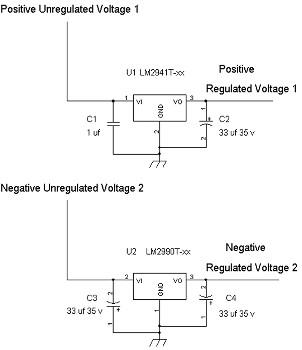
FIGURE 9.36 LDO regulators with decoupling capacitors larger in capacitance for C2, C3, and C4 when compared to standard voltage regulators.
The available fixed-output voltages for the positive voltage LDO regulators LM2940T-xx are: 5 volts, 8 volts, 9 volts, 10 volts, 12 volts, and 15 volts. For example, a positive 5-volt version would be listed as LM2941T-5.0, whereas a 9-volt version would be LM2940T-9.0, and a 12-volt part number will be LM2940T-12.
For the negative voltage LDO regulator LM2990T-xx, the available fixed-output voltages are: –5 volts, –12 volts, and –15 volts. An example part number for a –5-volt version would be listed as LM2990T-5.0, whereas a negative 12-volt version would be LM2990T-12.
Things That Can Go Wrong with 7800 and 7900 Series Voltage Regulators
• If the input voltage to a positive voltage regulator (e.g., 7805) is a negative voltage that is the wrong polarity, the positive voltage regulator will drain excessive current and the output will be about –0.9 volts. You will need to shut off power immediately and replace the regulator with a new positive voltage regulator. You then connect with the correct polarity input voltage (e.g., a positive voltage) to the input of the new positive voltage regulator.
• If the input voltage is correctly positive, but the ground lead (e.g., middle lead) is left unconnected (e.g., floating), the output voltage will be roughly the same voltage as the input. This can lead to damaging ICs or circuits that require a regulated voltage. For example, suppose you have a TLC272 op amp that is connected to a +12-volt regulator’s output, 7812, but the 7812’s middle ground lead is not connected to ground. With an input voltage of +24 volts, the output voltage of the 7812 will be about 23 volts, which will damage the TLC272 op amp because it has a maximum operating voltage of 16 volts.
• If you reverse the pin outs by swapping the input and output leads of a positive voltage regulator (e.g., 7805) while still grounding the middle lead, then you will be applying the unregulated voltage to the output pin and taking the output of the regulator via its input pin. This will cause excessive current and also pass the unregulated voltage from the regulator’s output pin to the regulator’s input pin. In other words, you will be applying an unregulated high voltage to your circuits, which can damage them. Swapping the positive voltage regulators’ two outer leads can be the result of not paying attention to the silkscreen on a printed circuit board that denotes which way the TO-220 package is installed. Power should be turned off immediately and the regulator replaced and installed properly.
• If the input voltage to a negative voltage regulator (e.g., 7905) is an incorrect positive voltage of the wrong polarity, the negative voltage regulator will drain excessive current and the output will be about +2 volts. You will need to shut off power immediately and replace the regulator. Then fix the wiring of the input voltage source such that it provides a negative voltage to the input pin of the negative voltage regulator.
• If the input voltage is correctly a negative voltage, but the ground lead (e.g., first lead on the left side) is unconnected (e.g., floating), the output voltage will be roughly the same negative voltage as the input’s negative voltage. Hence the raw input voltage is passed onto the circuits requiring a well-defined or limited negative voltage. This can lead to damaging ICs or circuits that require a regulated negative voltage.
• If you reverse the pin outs by swapping the pin sequence from 1, 2, 3 to 3, 2, 1 of a negative voltage regulator (e.g., 7905), the output lead will be grounded, the input lead stays the same since it is the middle pin, and output is now provided via the ground pin. This will cause excessive current and output of about –0.7 volt. You will need to shut off power immediately and replace the regulator with the correct pin out sequence.
Accidents Involving the 7800 Series Positive and 7900 Series Negative Voltage Regulators
If you load onto a printed circuit board a positive 78xx voltage regulator in the place of a negative 79xx voltage regulator and 79xx regulator in the place of a 78xx voltage regulator, you will have fed through the raw voltage with a voltage drop of about the rated regulated voltage.
For example, if 7808 is installed in the place of a negative voltage regulator, 79xx, and the raw supply is minus 20 volts, then the output voltage will be –(raw voltage – rated regulated voltage), which is then: –(20 volts – 8 volts) = –12 volts.
And if a negative voltage regulator such as a 7906 is installed where a positive voltage 78xx regulator should be, the output voltage will be (raw voltage – rated regulated voltage) = (20 volts – 6 volts) = +14 volts.
If the raw positive voltage is equal to or less than the regulated voltage rating, the output will be close to zero for the 7900 negative series regulator that is loaded into a board that is meant for a 7800 series regulator.
Some Mishaps with Low–Drop-Out LM2940 and LM2990 Series Regulators
The low–drop-out (LDO) regulators have different internal circuitry as the standard regulator circuits. Thus, there will be some differences when LDO regulators are connected incorrectly.
• When a positive voltage LDO regulator (e.g., LM2940-xx) is connected with the input and output leads swapped, and a correct raw positive voltage is applied, the regulator will pass through the raw positive voltage. For example, if the raw voltage is +20 volts DC, and the input and output leads of the LDO positive voltage regulator is swapped, the output voltage will be about +20 volts. Therefore, there will be no regulation, and subsequent circuits requiring a regulated voltage may be damaged. You should turn off the raw power supply and replace the LDO and install a new one with the correct pin out sequence.
• If you apply a negative input voltage to a positive voltage LDO’s input terminal, the output will be close to zero volts.
• If you forget to connect the middle terminal of the positive voltage LDO to ground and leave the middle pin unconnected or floating, again the output will be essentially the unregulated input voltage that can cause damage to other circuits.
• If you have inadvertently installed a negative LDO (e.g., LM2990-xx) in place of a positive voltage regulator, and turned on the positive raw supply, the negative voltage LDO will pass to its output the raw input supply voltage. This raw input voltage will be higher than the expected regulated voltage and can damage other circuits.
• For a negative LDO voltage regulator (e.g., LM2990-xx), if you apply an incorrect positive voltage at the input, the output will be about +1 volt from the negative LDO regulator, and excessive current will draw. The raw power supply must be turned off immediately. Then the correct negative supply must be wired to the input terminal.
• If you reverse the pin sequence of the negative LDO voltage regulator, excessive current will be drained and about –0.7 volt will be at the output. Again, turn off the supply immediately and install a new negative LDO voltage regulator with the correct pin out sequence.
• If the circuit requires a negative LDO voltage regulator and everything is connected correctly, but a positive LDO voltage regulator is mistakenly installed, the raw supply voltage will pass to the output and possibly cause overvoltage damage to other circuits.
Some Troubleshooting Hints When Working with Regulators
• One thing to remember about voltage regulator chips is that they can only deliver current in one direction. In a positive regulator, the current flows out. But if you try to have the positive voltage regulator absorb or sink current, you may turn off the voltage regulator and as a result, the output voltage will no longer be the expected regulated voltage. An example is if you have a +5-volt regulator (7805) and if one end of a resistor is connected to the output of the 7805 and the other end of the resistor is connected to +20-volt source, then current will be flowing the wrong way into the output terminal. This can cause the 7805 to shut off because it can only absorb a small amount of current.
• If the voltage regulators get too hot, then they will shut down and output close to zero volts. You will need to first check if you have the correct voltage regulator installed accordingly. Then you need to monitor the current into the voltage regulator’s input terminal via an ammeter. See if it’s within the range of the output current capability of the voltage regulator. If it is, then the voltage regulator may need to be mounted on a heat sink.
• If the output is lower than the regulated voltage, use a DVM and measure the voltage at the input and output terminals. For a positive voltage regulator, the input voltage should be greater than 2 volts above the rated output voltage. For example, if you are using a 7808 for +8 volts output, the minimum input voltage is 2 volts above that, which means that the input voltage is greater than or equal to 10 volts.
• If you are monitoring with an oscilloscope on the input and output terminals and there is a high-frequency oscillation signal, then make sure you have the decoupling capacitors soldered or wired within one-half inch of the input, ground, and output terminals. Also make sure the capacitances are large enough (≥ 1 μf ).
If you are using ceramic capacitors, use a voltage rating at least twice the voltage at the input and output terminals. This is because some ceramic capacitors will de-rate when there is a DC voltage close to its maximum rating.
Should an electrolytic capacitor be used, observe its polarity. If it is installed incorrectly, shut off the power immediately and install a new one with the correct polarity.
This completes Chapter 9, and we will be looking into audio circuits in the next chapter.