CHAPTER 13
![]()
Timer, CMOS, and Motor Drive Circuits
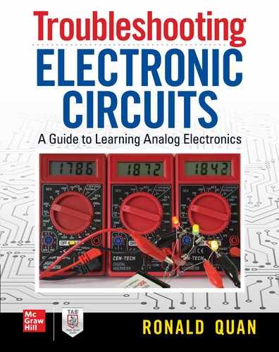
We will be looking into analog timing and oscillator circuits that use the NE555/LM555 (a.k.a., 555 circuit or chip) integrated circuit. Although this circuit was manufactured in the early 1970s, it still finds many uses in hobbyist circuits and projects. The 555 circuit is an 8-pin integrated circuit that can be configured into many different circuits. For example:
• A timing circuit to provide a fixed duration pulse when triggered by an external signal (e.g., closing a switch). The 555 can be configured as a one-shot circuit to generate pulses.
• 555 oscillator circuits.
• A simple CMOS (complementary metal oxide silicon) oscillator that includes a 555 pulse-width modulator circuit for driving a motor via a switch mode bridge amplifier.
Types of 555 Timer Chips
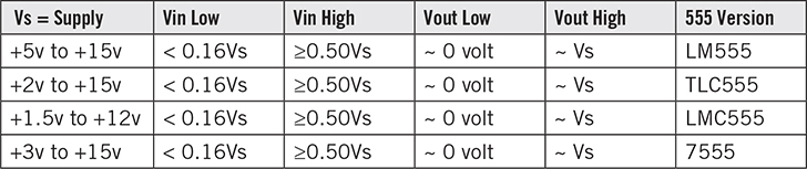
Before proceeding with some of the circuits, we should be aware that there are two types of 555 timer chips—bipolar transistor and complementary metal oxide silicon (CMOS).
The original design in the 1970s was done with bipolar transistors that had part numbers such as NE555, LM555, CA555, MC1455, and MC1555. This chip generally worked over a 5-volt to 15-volt power supply. One of its advantages is that the output signal can drive at 100 mA safely, and if pushed, up to 200 mA. Its disadvantage is that the standby current is in the 3-mA to 10-mA range for supply voltages at 5 volts and 15 volts, respectively. Top oscillation frequency of the bipolar 555 chip was about 500 kHz to 1 MHz.
By the 1980s the 555 integrated circuit was offered in CMOS, which dramatically reduced the standby current to less than 500 μA (200 μA typical at 5 volts supply). Typical part numbers were the TLC555, LMC555, and ICM7555 (or 7555 for a short-handed name). The CMOS version offered a higher oscillation frequency at about 2 MHz, which is twice the “speed” of the bipolar version. Later, an even faster CMOS version was available as the LMC555 that provides up to 3-MHz oscillation frequency. Although the ICM7555 guarantees at least a 500-kHz oscillation frequency, its data sheet chart shows oscillating frequencies of 2 MHz or 3 MHz.
The CMOS 555’s power supply voltage range expanded to the low end starting at 2 volts while still having a maximum 15-volt rating. Output sourcing current is reduced to 10 mA, which means its drive current is only about 5 percent of the bipolar transistor version, LM555. However, it can sink or absorb about 100 mA at its output, which means if the load such as a relay’s first terminal is connected to 15 volts, and the relay’s second terminal is connected to the TLC555’s output terminal, the relay can have up to 100 mA flowing through it.
NOTE: When connecting a relay in this manner, also connect a diode such as 1N4002 where the cathode is connected to the +5-volt supply and the anode is connected to the output pin of the TLC555 to suppress high voltage spikes from the relay coil.
Basic Modes of the 555 Timer Chip and Pin Outs
Figure 13-1 shows the 8-pin assignments for the 555 timer bipolar and CMOS chip, and also three basic operations.
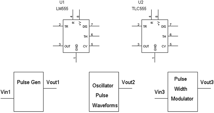
FIGURE 13.1 Pin outs for the bipolar LM555 and CMOS TLC555 integrated circuits and three basic modes of this timer chip.
As we can see in Figure 13-1, the bipolar (LM555) and CMOS (TLC555) versions have the same pin outs and they can in general be used interchangeably. In most cases the reset pin 4 is tied to the 1V pin 8 to enable the 555 circuit. To reset the output pin 3 to a low-logic level, the reset pin 4 must to be coupled to ground via a resistor (e.g., ≤ 1000Ω) or a wire.
The 555 timer chip can perform at least three basic functions as shown in Figure 13-1. This chapter will focus on it being a pulse generator (e.g., one-shot timing pulse) for an input pulse signal Vin with an output signal, Vout, an oscillator (Vout2), and a pulse-width modulator with an input modulating signal Vin3 with a pulse-width modulated signal at Vout3. Note that the pulse-width modulator may include a potentiometer for providing a modulating signal.
To make a timing pulse the 555 chip generally requires logic low (e.g., 0 volts) and logic high (e.g., 1V or the supply voltage) for Vin1 at pin 2 of the 555 chip to output a fixed duration pulse, Vout1 at pin 3. The output pulse starts when the input Vin1 goes from the high to low logic states such as 15 volts to 0 volts when the supply voltage 1V = 15 volts. For example, you can make an LED or relay turn on for a fix duration when Vin2 is switched from 15 volts to 0 volts. When Vin1 goes from 0 volts to 5 volts, there is no change in Vout1. Only “negative” going transitions (e.g., 15 volts to 0 volts) will trigger an output signal having a fixed duration pulse at pin 3 (Vout1).
For the oscillator function, the 555 chip will output a pulse waveform at Vout2. The oscillation frequency ranges from less than 1 Hz to at least 500 kHz. The duty cycle of the output signal can be adjusted anywhere from a narrow negative going pulse to nearly a square-wave signal (~50 percent duty cycle).
The 555 chip can also be used to provide pulse-width modulated pulses. By pulse-width modulation we mean that the frequency of the output waveform does not change, but the output signal’s duty cycle or pulse-width varies according to a modulation or control voltage input signal at Vin3.
The 555 Pulse Generator (a.k.a., One-Shot or Monostable Mode)
This 555 pulse generator circuit provides a fixed duration output pulse for an input signal that transitions from high to low logic levels (e.g., 15 v to 0 v). See Figure 13-2 where the 555 circuit is configured in “monostable” or pulse generator mode.
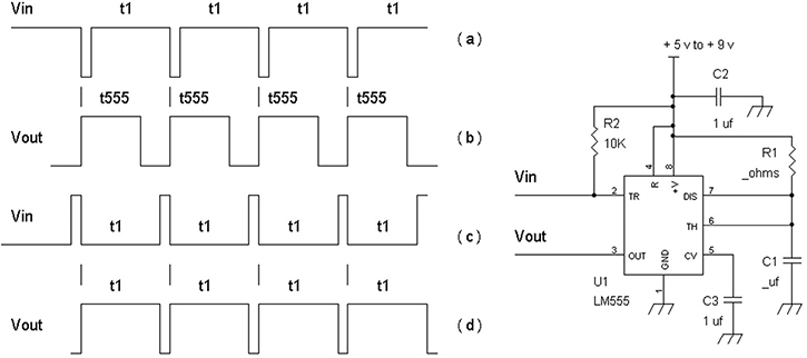
FIGURE 13.2 Input waveforms (a) and (c), and output waveforms (b) and (d) respectively with a schematic diagram of the monostable timing pulse generator.
A “proper” input waveform for Vin is one that has narrow low logic voltage pulse-width that is shorter in duration than the output high logic state. In Figure 13-2(a) for Vin, the negative going pulse is shorter in duration than the output pulse’s duration of t555. With the proper waveform, the output positive cycle pulse width is t555 ~ 1.1 R × C1 = τ.
However, if the input waveform has a longer duration low logic voltage, such as in Figure 13-2(c), where its duration t1 > t555, the output of the timing chip at pin 3 will result in a longer positive pulse of duration t1 of Figure 13-2(d) even though the pulse-width should really have a duration of t555 shown in Figure 13-2(b).
From a top overview of the 555 monostable pulse generator circuit, we see that the input signal into pin 2 (trigger input) requires a negative going transition to output a fixed duration pulse. This fixed duration pulse is logic high and has a time length of τ ~ 1.1 R1 × C1, where τ is measured in seconds, R1 is measured in ohms, and C1 is measured in farads. For example, suppose we want to generate a 1 msec pulse (one thousandth of a second) or 0.001 second. We then have 0.001sec = 1.1 R1 × C1.
Suppose we first choose R1 = 1000Ω, then we can solve for C1 as:
C1 = 0.001 sec/(1.1 × R1) = 0.001/(1.1 × 1000Ω) → C1 = 9.09 × 10⁻⁷ farad
C1 = 0.909 × 10⁻⁶ farad
But 10–6 farad = 1 μf, so C1 = 0.909 × 1 μf, or C1 = 0.909 μf, which is a non-standard value.
If we can scale R1 by (1/1.1), R1 → 909Ω = 1000Ω/(1.1). This will get rid of the 1.1 factor in C1 = τ /(1.1 × R1). With R1 = 909Ω ~ 910Ω, then with R1 5 910Ω we have: C1 = 0.001sec/(1.1 × 910Ω) ~ 0.001 sec/(1000Ω) or C1 5 1 μf, a standard capacitance value.
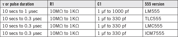
One question to ask: Is there a safe range of resistance values for R1? For example, it probably would not be a good idea to make a 1 msec pulse generator with R1 = 0.91Ω and C1 = 1000μf because with R1 being less than one ohm, the circuit will have to draw several amps of current because the voltage at C1 varies between zero volts and one-third (e.g., 1⁄3) the supply voltage. For example, if 1V = 15 volts and R1 = 0.91Ω, the voltage at C1 has to be in a range of 0 volts to 15 volts 3 1⁄3 or 0 volts to 1.66 volts. Since R1 is connected to 1V and C1, this means the voltage across R1 is (15 volts – 1.66 volts) or 3.33 volts, or (15 volt – 0 volts) or 5 volts. The current flowing through R1 would then be in the range of 3.33 volts/0.91Ω to 5 volts/0.91Ω or 3.66 amps to 5.49 amps. Most likely, the 555 circuit may be damaged or it may go into a current limiting mode. Either way, there would be no correct output signal or pulse at pin 3. Table 13-1 shows some suggested value ranges for R1 and C1 based on the output pulse duration.
TABLE 13.1 Suggested Values for R1 and C1
In Figure 13-2, capacitor C3 is a decoupling capacitor to ensure that the output pulse from pin 3 does not jitter due to noise coming through the power supply. If the power supply into pin 8 has ripple or other noises, C3 may have to be changed to a higher capacitance value such as an electrolytic capacitor, 33 μf at 25 volts, where the positive terminal of C3 is connected to pin 5 and the negative terminal of C3 is connected to ground. In general, the 555 timer chip should be powered by a regulated voltage to supply a “noise free” voltage to pin 8. However, this integrated circuit may be powered by batteries, which do not have ripple or noise. But be aware that a battery will slowly drop in voltage as it is supplying current to the 555 circuit.
The input level that triggers this one-shot circuit is at one-third the supply voltage, so to be on the safe side, the input signal should be between 50 percent to 100 percent of the supply voltage for a logic high voltage, and below one-sixth of the supply voltage for a low logic state. For example, if 1V = 5 volts, then a “safe” logic high voltage is between 2.5 volts and 5 volts, and a “safe” logic low voltage is between 0 volts and 1833 mV. The trip voltage is one-third of 5 volts or 1.66 volts, which means this voltage as an input voltage to pin 2 should be avoided or there will be “noise” or chatter at the output pin 3.
Table 13-2 shows some suggested low and high logic levels along with corresponding output levels.
TABLE 13.2 Input and Output Voltages for 555 Circuits Configured as a One-Shot or Monostable Circuit
Troubleshooting the 555 One-Shot Monostable Timer
1. With the circuit in Figure 13-2, find the DC conditions first using a voltmeter, or with an oscilloscope in the DC coupling mode set to 2 volts per division. Measure voltages with a voltmeter at pins 8 and 4 that should be the supply voltage, such as +5 volts (or some other positive supply voltage ≤ 15 volts). Confirm that the voltage at pin 1 that should be connected to ground is zero volts.
2. Now measure the DC voltage at pin 5; the control voltage pin should be 67 percent of the power supply voltage. For example, if pins 8 and 4 have +5 volts on them, then pin 5 should have 67% × 5 volts or 3.33 volts DC within 15 percent.
3. Connect a square wave signal generator that has a DC voltage swing from 0 volts to 5 volts to pin 2 of the 555 timer chip. To set the frequency of the signal generator, first determine the pulse width, pw = 1.1 R1 × C1. Set the signal generator’s frequency to fgen = 0.75/pw. For example, if the pulse width is pw = 0.001 sec or 1 millisecond, set the generators frequency fgen = 0.75/0.001 or fgen = 750Hz. Confirm that the output at pin 3 produces a positive pulse whose width is 1 msec at a 750 Hz rate.
4. Alternatively, if you do not have a signal generator and just want to see if the 555 chip is working, connect a voltmeter (DVM) to pin 3 and ground, where the positive test lead is at pin 3 and the negative test lead is connected to ground. Make sure pull-up resistor R2 in Figure 13-2 is installed. We are now going to make an 11-second timer. Let R1 = 1MΩ, and let C1 = 10 μf where the (+) terminal of the C1 is connected to pins 6 and 7. The DVM should be reading close to zero volts at pin 3. Now short pin 2 to ground temporarily for less than 1 second, then observe the DVM is at a logic high voltage > 3 volts DC for about 11 seconds. You can use a watch or a clock to measure the time. If this is OK within ± 30 percent, the circuit works. Be sure to measure both R1 and C1 if possible with a DVM (e.g., Extech MN26 or equivalent DVM). If you do not have a DVM, you can connect pin 3 to a series resistor (e.g., 470Ω to 4700Ω) to an LED (e.g., red, yellow, or green having about a 2-volt turn-on voltage). See Figure 13-3. The LED should be turned on for about 11 seconds. Then replace R1 and C1 with the original values. Again the output turn on time for an input signal from high to low logic states (e.g., input signal from =5 volts to 0 volts) is τ = 1.1 RC.
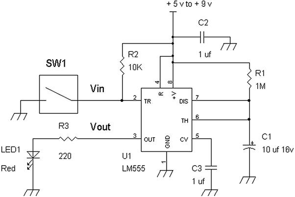
FIGURE 13.3 Switch SW1 is a momentary switch and it is closed circuit to ground for a split second, which should then turn on LED1 for about 11 seconds.
When You Want to AC Couple a Signal to Trigger a Pulse Output Signal
Figure 13-4(a) shows a simple DC restoration circuit with C3, CR1 and R3, and Figure 13-4(b) shows AC coupling methods to trigger pulses via a voltage divider circuit R2 and R3.
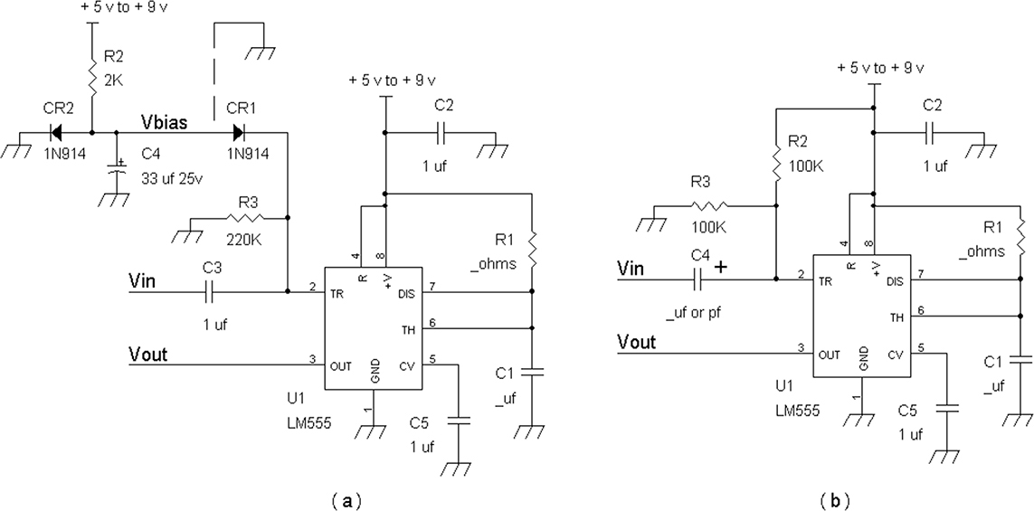
FIGURE 13.4 (a) AC coupling via a DC restoration circuit via C3, CR1, and R3 with Vbias ~ 0.7 volt; (b) AC coupling signals via a biasing network R2 and R3.
In both circuits, the input signal should have a peak to amplitude equal to the supply voltage of the 555 circuit. For example, if the supply voltage is 5 volts, the input signal Vin should be in the order of 4 volts to 5 volts peak to peak. However, it turns out that the input signal must have its negative cycle duration less than the 555’s time output pulse duration of τ = 1.1R1 × C1, or the output pulse at pin 3 will be longer than the expected duration of τ = 1.1R1 × C1.
Figure 13-4(a) shows a negative peak DC restoration circuit where the negative peak of Vin is set to 0 volts via the DC restoration diode CR1. This means if Vin is a signal that has no DC offset or any DC offset voltage, the DC restoration circuit CR1 at its cathode will provide a signal “clamped” to 0 volts for the negative peak portion of Vin. This effect is useful when the incoming waveform (e.g., a pulse signal) with low or high duty cycle is used. DC restoration is often used to level shift a signal to a particular or well-defined negative cycle voltage. For example, if the following (Vin) incoming 5-volt peak to peak signal has a range of –2.5 volts to +2.5 volts, –5 volts to 0 volts, +5 volts to +10 volt, etc., the DC restoration circuit at the cathode of CR1 will provide a signal that ranges from 0 volts to +5 volts, a standard logic level range for a 5-volt system.
The circuit in Figure 13-4(b) allows AC coupling to the trigger pin 2 at 50 percent at the power supply voltage. Generally, C4 as 33 μf will work, but this large capacitance value can be a problem if Vin is a signal that has a longer negative cycle duration than τ = 1.1R1 × C1. For example, suppose we have τ = 1.1(910Ω) × 1μf = 1 msec. If Vin is a pulse whose negative cycle exceeds 1 msec, then the output signal at pin 3 will be longer than 1 msec. However, we can fix this by lowering the capacitance of C4 to about 220 pf to narrow the width of Vin. See Figure 13-5 for a comparison between having C4 = 33 μf and C4 = 220 pf.
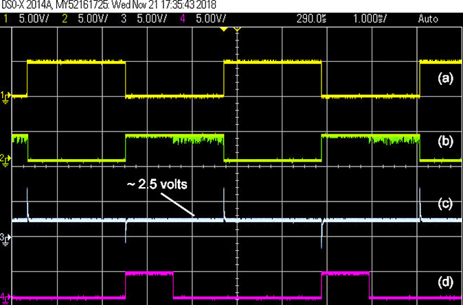
FIGURE 13.5 Comparing C4 = 33μf and C4 = 220 pf on (d) shows a more reliable output waveform, which conforms to τ = 1.1 R1 x C1 for the output pulse-width, than (b), which is longer than τ = 1.1 R1xC1.
With reference to the circuit in Figure 13-4(b) that uses AC coupling with C4, we see that with C4 = 33 μf, the waveform at pin 2 of the 555 chip is shown in Figure 13-5(a). This waveform is a square-wave signal, whose negative cycle duration is longer than τ = 1.1 R1 × C1 ~ 1 msec in this example. As a result of this longer duration negative cycle pulse the resulting output waveform is longer than τ = 1.1 R1 × C1 as shown in Figure 13-5(b). If we have instead C4 = 220 pf, then we see in Figure 13-5(c) that the negative going pulse is much narrower. The “flat line” in (c) is at 2.5 volts so that the negative going spike will easily go below the threshold voltage of 1.66 volts (e.g., 33 percent of the 5-volt supply) to trigger the correct duration pulse shown in Figure 13-5(d).
“Strange” Output Signals Observed via an Oscilloscope
We will now show two cases of pin 3 output signals in the monostable mode (one shot) where you can observe a high-frequency oscillating waveform from the 555 timer chip. See circuits in Figure 13-2 or Figure 13-4. The first example shows what happens when you forget to install the timing capacitor, or install the timing capacitor (e.g., C1) with an incorrect value where C1 ≤ 20 pf. See Figure 13-6, second trace from the top. The fix for this is rechecking your wiring and reading the capacitor’s marking, then installing the correct value capacitor that is typically in a range of 1000pf to 10 μf.

FIGURE 13.6 Completely gated oscillating waveform when C1 has insufficient capacitance. Top trace is the input signal, bottom trace is the output waveform.
If you also forget to wire a timing capacitor for C1, then you may see an output waveform on pin 3 as shown in Figure 13-6. Also, make sure the 555 pins 6 and 7 are connected.
The second error we will show is where the input signal’s frequency and pulse-width can “force” the output signal at pin 3 to give out a slightly gated oscillating signal due to having a longer duration negative going pulse. See Figure 13-7, bottom trace. As a reminder, you can fix this problem by using the circuit in Figure 13-4(b) where C4 is a capacitor between 100 pf and 1000 pf to provide a narrowed negative going pulse into input pin 2 of the 555 chip.
5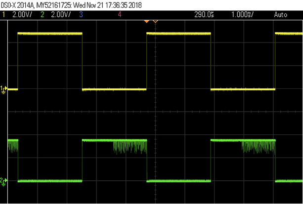
FIGURE 13-7 Top trace is the input signal and the bottom trace is the output waveform with noise.
Troubleshooting the 555 Oscillator (a.k.a. Astable Mode)
We now turn our attention to the 555 circuit configured as an oscillator with some troubleshooting methods. See Figure 13-8.
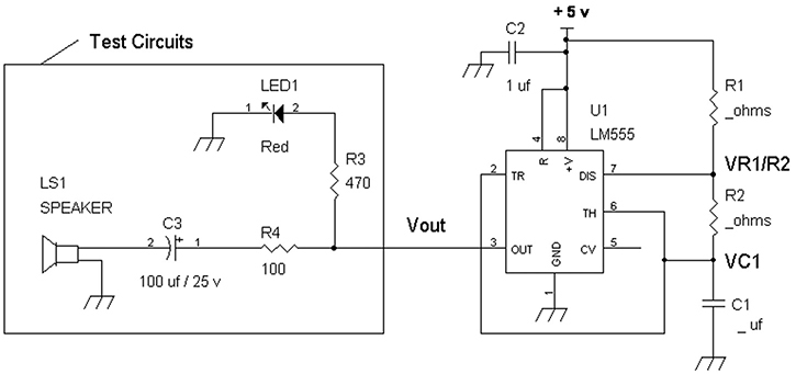
FIGURE 13.8 A 555 configured as an oscillator with test circuits including an LED and a speaker.
A 555 timer can oscillate at sub 1 Hz frequencies to at least 500 kHz. The frequency is determined by f = 1.44/[(R1 + 2 × R2)C1]. For example, if C1 = 0.01 μf, R1 = 100kΩ, and R2 = 51kΩ, then f = 1.44/[(100kΩ + 2 × 51kΩ)(0.01 × 10⁻⁶ F)], or f = 713 Hz. See Figure 13-8.
To confirm that the 555 circuit is oscillating within the audio range (e.g., 20 Hz to 15 kHz), you can use a loudspeaker (LS1) with an output coupling capacitor C3 and series current limiting resistor R4. The reason for the limiting resistor is to prevent the 555 chip from delivering excessively unsafe current that can damage its output circuit at pin 3.
Most speakers (LS1) have low voice coil impedance in the range of 4Ω to 8Ω. Thus, the speaker should not be connected directly to pin 3 of the 555 timer chip and ground for two reasons. One is to prevent loudspeaker damage, and the second is to avoid burning out the timer chip. A 555 circuit driving directly a load resistance of 4Ω to 8Ω is almost like shorting the output pin 3 to ground DC-wise. To prevent excessive DC currents flowing out of pin 3 of the 555, we need to add a series capacitor, C3, as shown in Figure 13-8. For low-impedance speakers, usually C3 ≥ 33 μf, with it typically being 100 μf to 470 μf.
If the 555 is set to lower frequencies below 1 Hz you can use an LED and observe the flashing rate. But you should also be able to hear the speaker “click” at the oscillation frequency such as 1 click per second if the frequency is 1 Hz. Finally, if you have an oscilloscope, you can probe VC1 and VR1/R2, which will have signals with an AC component such as an oscillating waveform.
If the 555’s oscillation frequency is higher than the (human) audio hearing range, then you can divide the oscillation frequency to provide an audible tone. See Figure 13-9. Alternatively, you can connect/solder a “transmitting antenna” wire of a few inches to 15 inches to pin 3 and place this wire close to an AM radio to sense the oscillator. Generally, as you tune the AM radio, you will hear a reduction in hiss when the radio is tuned to a frequency related to the 555’s oscillation frequency, or to a multiple (e.g., harmonic) of the oscillation frequency.
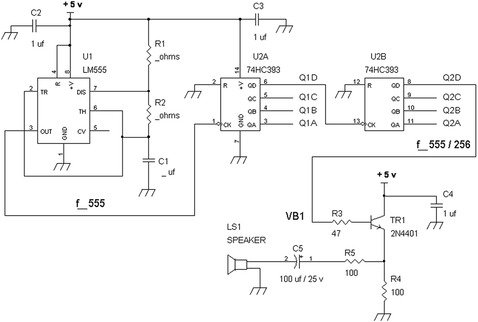
FIGURE 13.9 A 555 circuit with a frequency divider by 256 circuit using binary counters.
In Figure 13-9, the 555’s output signal is connected to frequency divider U2A at its clock input pin 1, which provides square-wave signals at one-half (Q1A), one-quarter (Q1B), one-eighth (Q1C), and one-sixteenth (Q1D) of the 555’s frequency. The resistor R3 as shown is connected to Q2D but can be connected to any of the signal outputs from Q1A to Q1D or from Q2A to Q2D. The output at Q1D is then fed to the second frequency divider clock input (pin 13) of U2B.
U2B continues the chain of frequency division to one–thirty-second (Q2A), one–sixty-fourth (Q2B), one–one hundred twenty eighth (Q2C), and finally one–two hundred and fifty sixth (Q2D). For example, if the 555 is set to 1 MHz, then the signal at Q2D will be 1 MHz /256 or 3.906 kHz, which would be an audible tone.
Of course, if you have an oscilloscope, you do not need to have U1A, U1B, and the associated speaker amplifier of TR1 with the speaker LS1. You can just probe the waveform at pin 3 of the 555 integrated circuit.
One More Example on Driving Speakers with the 555
You’ll notice that the loudspeaker in Figures 13-8 and 13-9 uses a DC blocking capacitor. There is a good reason for this. Some circuits have the speaker driven by the 555 via a resistor to the pin 3 output. This will cause excessive DC current drain and also send a DC current into the loudspeaker, which can heat up its voice-coil unnecessarily. See Figure 13-10(a) and see the solution in 13-10(b).
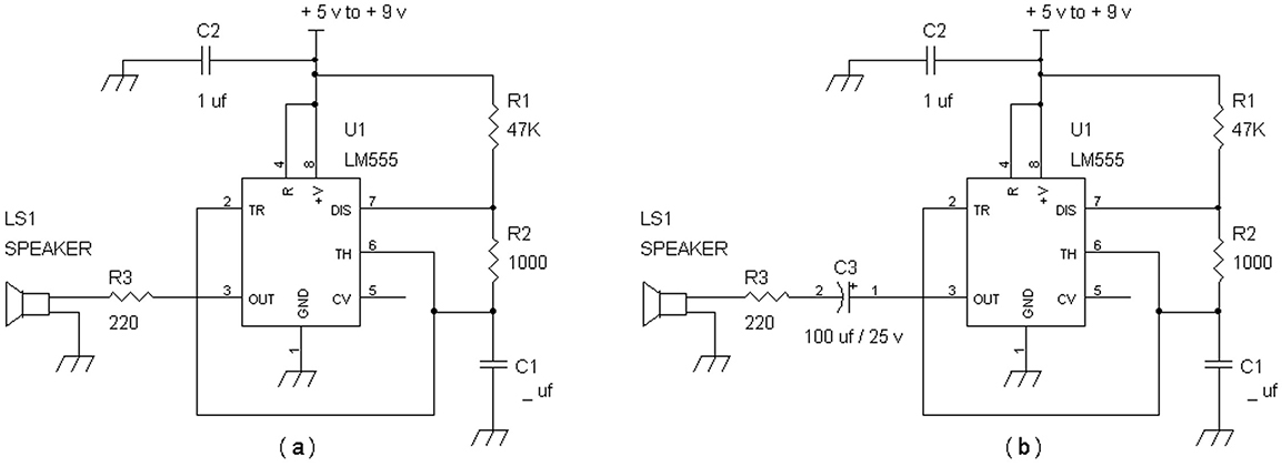
FIGURE 13.10 (a) The 555 is DC coupled to the speaker that causes a problem, and (b) a coupling capacitor, C3, blocks DC current.
When the series current limiting resistor R3 is in the order of a couple of hundred ohms, the loudspeaker can tolerate some DC current flowing into it. With 220Ω for R3 in Figure 13-10(a), the average DC voltage at pin 3 of the 555 is about 2 volts to 3 volts DC, depending on the values of R1 and R2, which determines the duty cycle of the output signal. With 2 to 3 volts DC at pin 3, there is then about 9 mA to 13 mA DC flowing into the loudspeaker LS1. This is power wasted. However, by using a coupling capacitor, C4, as shown in Figure 13-10(b), any DC current flowing into speaker LS1 is reduced to zero; and this then saves power because there is no 9 mA to 13 mA of DC current being wasted.
If the 220Ω resistor needs to be lowered to 47Ω so that the speaker produces a louder sound, then Figure 13-10(a)’s circuit will drain about 2.0v/47Ω to 3v/47Ω or 42 mA to 63 mA of wasted DC current. Having the DC blocking capacitor C3 in Figure 13-10(b) will then reduce the DC current to zero, while allowing the speaker LS1 to produce a louder sound.
Why Again an Output Coupling Capacitor Is Preferable
A 555 configured as an oscillator can be used to build a high-voltage converter. For example, with a 6-volt DC supply to the 555 circuit, you can make a greater than 60-volt DC source. This circuit uses a step-down 110-volt to 6-volt AC transformer in reverse to form a step-up from 6 volts AC to 110 volts AC. See Figures 13-11 and 13-12.
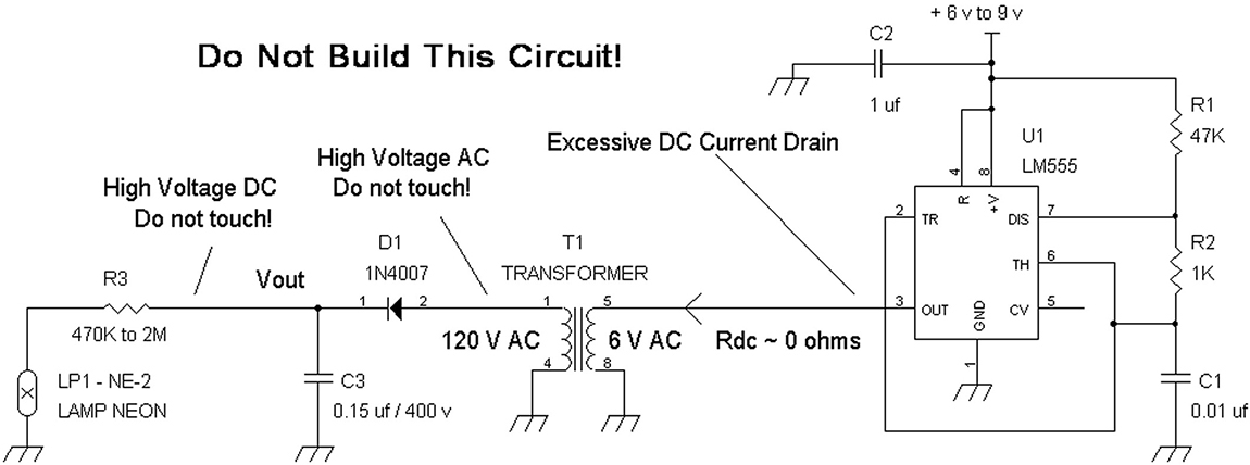
FIGURE 13.11 A high-voltage power supply that may draw excessive current.
First, please DO NOT BUILD Figure 13-11’s circuit because it will drain excessive DC current from the 555 output pin 3. In terms of DC current, the transformer’s 6 V AC winding (T1), has close to zero DC resistance. The duty cycle of the negative pulse is R2/(R1 + 2R2), and in Figure 13-11 we see that R1 = 47KΩ and R2 = 1KΩ, so the negative pulse duty cycle is 1K/(47K + 2 × 1K) = 1K/(47K + 2K) = 1/49 or about 2 percent. This then means that the positive pulse’s duty cycle is then 100 percent minus 2 percent or about 98 percent. Because the 555 output pin 3 is a signal that is at least 98 percent duty cycle for the positive going pulse, this means that the average DC voltage is approximately 98 percent of the 555 power supply.
For example, if the supply voltage is 7.2 volts (six rechargeable 1.2-volt cells in series), the average DC voltage at pin 3 will be 7.2 volts × 98 percent or +7.05 volts DC. Because the 6 V AC winding of T1 is a DC short circuit to ground, the 555’s pin 3 will try to supply 7.05 volts to ground in terms of DC. This will then cause the 555 to go into current limiting, while not providing the correct output AC signal into T1. This is why we do not want to build the circuit in Figure 13-11, unless we fix it in terms of blocking DC currents from flowing via pin 3 of U1.
Again, please do not build the circuit in Figure 13-11, as it may cause damage to the 555 circuit. However, if we just add an AC coupling capacitor, C4, as shown in Figure 13-12, we avoid draining excessive DC current from output pin 3 of the 555 circuit.
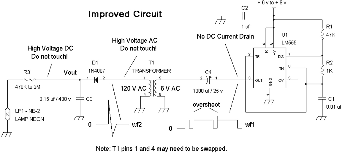
FIGURE 13.12 A high-voltage power supply with improved efficiency by using a DC blocking capacitor, C4. Note: wf1 < 15 volts peak to peak and wf2 > 100 volts peak to peak.
In Figure 13-12, you can troubleshoot the circuit by using an oscilloscope and observing the waveforms, which have about a 2-kHz frequency. From the pin 3 of the 555 chip, we see a large duty cycle pulse in “wf1”, waveform 1. It has DC levels from 0 volts to about the supply voltage minus about 1.2 volts. For instance, if the supply voltage is 16 volts the DC levels from wf1 is from 0 volts to (6v – 1.2v) = 4.8 volts. There will be some overshoot as shown in wf1 due to the inductive nature of the 6 V AC transformer winding. You can disconnect R3 temporarily and connect a DVM with 10MΩ input (e.g., a DVM that costs over $30 usually has a 10MΩ load resistance for the DC voltmeter setting) to D1’s cathode. The voltage at C3 and the cathode of D1 should be > 1100 volts DC when the supply voltage to the 555 chip is about 7.2 volts.
One “feature” to note in the waveform from pins 1 and 4 of T1 is that this voltage waveform is not symmetrical. See “wf2” in Figure 13-12, which is at the 120 V AC winding into D1’s anode when R3 is disconnected. As shown, the positive peak is about 60 percent larger in magnitude than the negative peak. For example, if the positive peak is about 1200 volts, the negative peak is about –125 volts. This means that you may get more voltage if you swap the leads of pins 1 and 4. When this circuit works properly and with R3 reconnected, the neon lamp may flicker or flash. This is normal since the filter capacitor, C3, provides very little current to the neon lamp, such that when the neon bulb lights up, it discharges C3’s voltage somewhat and then D1 has to build back up C3’s voltage to light the neon bulb. The neon has a firing voltage in the range of 95 volts or so. Below that, the neon bulb is not lit.
NOTE: Normally, in a power supply transformer such as in a 50 Hz or 60 Hz wall AC adapter, it does not matter which way you configure the leads because the AC voltage waveform is symmetrical. This means you get the same DC voltage after rectification and filtering regardless of the wiring orientation of the transformer. Swapping the leads here will give you the same DC voltage.
Average DC Level of Pulses
In Figures 13-11 and 13-12, the 555 timer outputs a high duty cycle pulse as shown in Figure 13-13(a), which produces a large average DC voltage, Vavg_hdc. In this example, the average level is almost the same as the logic high voltage, +V.
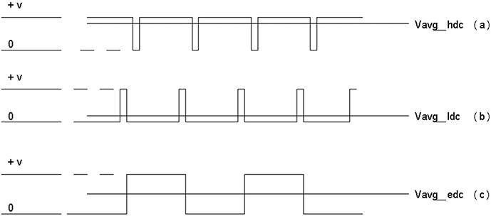
FIGURE 13.13 Respectively, average DC levels for (a) high, (b) low, and (c) even (50 percent) duty cycle pulse signals.
We see a high duty cycle waveform Figure 13-13(a) where the logic high level at +V stays on for a much longer time than when the waveform is at 0 volts. For pulses the average DC voltage is just the (duty cycle) × (+V), where duty cycle = (thigh_level)/(tlow_level + thigh_level), and where the frequency of the waveform is f = 1/(tlow_level + thigh_level). This also means (tlow_level + thigh_level) = (1/f). For example, a 1000 Hz signal will have as (tlow_level + thigh_level) = (1/1000 Hz) = 1 millisecond. Note that millisecond 5 msec.
So, if thigh_level = 0.9 msec, then tlow_level = 0.1 msec since the sum of tlow_level and thigh_level must equal 1 msec.
The duty cycle then is (thigh_level)/(tlow_level + thigh_level) = 0.9 msec/(0.1 msec + 0.9 msec) or the duty cycle is 0.9/1.0 = 90%. Thus, the average DC voltage will be (90 percent) × (+V). For example, if +V is 6 volts, then the average DC voltage for this signal is 0.9 × 6 volts = 5.4 volts.
For Figure 13-13(b), a low duty cycle waveform, we can have as an example, thigh_level = 0.1 msec, and tlow_level = 0.9 msec. The duty cycle then is (0.1 msec)/(0.9 msec + 0.1 msec) = 0.1/1.0 or the duty cycle is 0.1, which is 10 percent.
In Figure 13-13(c) an even duty cycle waveform is where tlow_level = thigh_level; and the duty cycle is always 50 percent since (thigh_level)/(tlow_level + thigh_level) = (thigh_level)/(thigh_level + thigh_level) = ½ or 50.
These waveforms in Figure 13-13 will help us understand the next section on switch mode signals (pulses) in motor drive amplifiers.
Using a 555 to Drive Motors via Pulse-Width Modulation
We now turn our attention to using a 555 circuit, used as a monostable one-shot circuit to vary the pulse width that will control the direction and speed of a motor. By changing the pulse-width (of a 20 kHz high frequency pulse signal) the duty cycle varies, which in turn provides a different average DC voltage. See Figure 13-14.
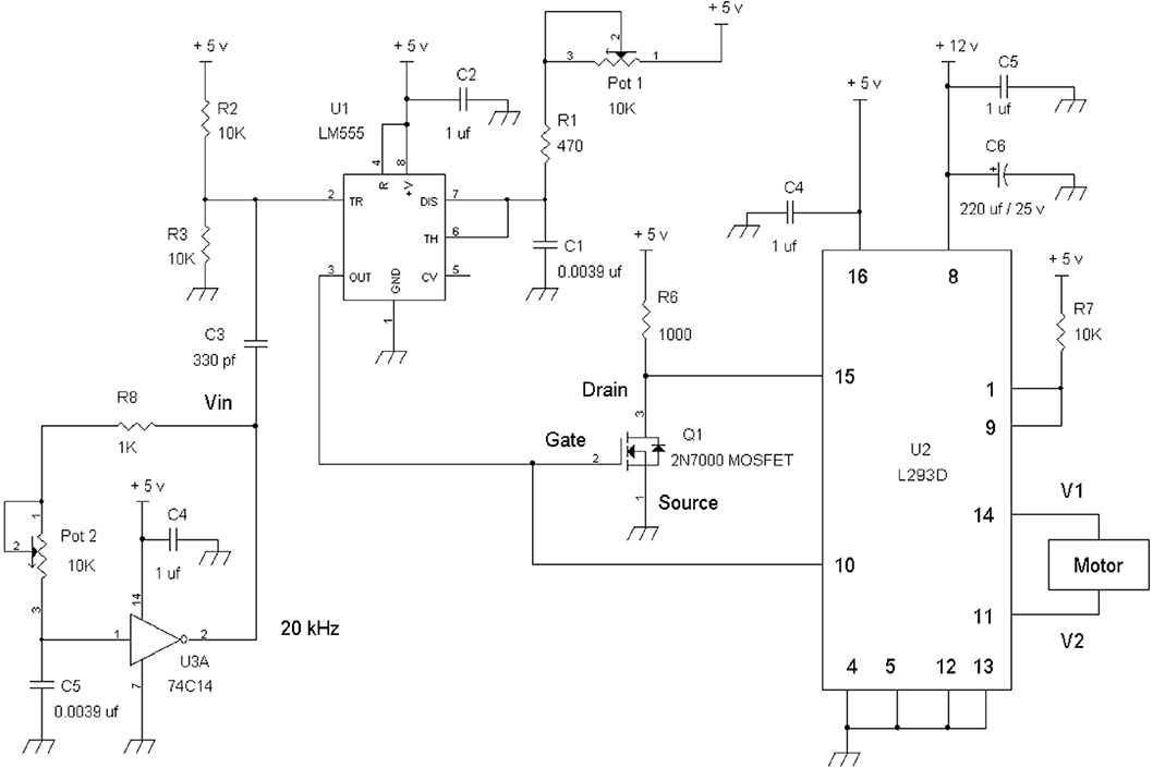
FIGURE 13.14 Motor drive circuit with Pot 1 for duty cycle adjustment to an H bridge amplifier.
This LM555 motor drive circuit was originally designed for an electronics class as an introduction to pulse-width modulation (PWM) signals. Instead of just using a DC power amplifier to drive the motor, a switching Class D amplifier is used because it has very high efficiency. The L239D chip sends out pulses of complementary duty cycle to the motor. For example, if V1 has an 80 percent duty cycle signal, then V2 has a 20 percent duty cycle pulse signal. Or if V1 has a 10 percent duty cycle pulse, then V2 has a 90 percent duty cycle signal. However, they can be equal when V1 has a 50 percent duty cycle pulse, which leads to a 50 percent duty signal for V2. The sum of the duty cycle of V1 and V2 must always total 100 percent.
Integrated circuit U2, L239D, is a bridge amplifier that receives pulse-width modulated input signals at pins 10 and 15. Because we want to be able to control the motor’s direction (forward or reverse), the motor is connected to the bridge output terminals corresponding to pins 11 and 14. For example, if pin 14 has a DC voltage, V1, while pin 11 (V2) is near zero volts, we will measure a positive voltage across the motor from pin 14 to pin 11. However, if the DC voltage at pin 14 (V1) is near zero volts and there is a positive voltage V2 at pin 11, then there will be a negative voltage measured across pin 14 and pin 11. A negative voltage implies a reverse direction. Also, if the voltage is the same at pin 14 and pin 11, then there is no net voltage (or potential difference) across the motor, and it has stopped turning.
NOTE: Please use a small 12-volt DC motor.
Now let’s look at Figure 13-14 starting with a relaxation oscillator U3A 74C14, which is a special logic inverter gate with Schmitt Trigger input characteristics. This type of input circuit allows for making an oscillator with a resistor (R8 1 Pot 2) and capacitor C5. The oscillation frequency is f ~ 1/[1.7(R8 1 Pot 2)(C5)]. If you know the oscillation frequency, f, and have chosen a capacitor, then the resistance can be found as: (R8 1 Pot 2) = 1/[1.7(f)(C5)]. If C5 = 0.0039 μf and f = 20 kHz, then (R8 1 Pot 2) = 1/[1.7(20 kHz)(0.0039 × 10⁻⁶ F)] or (R8 1 Pot 2) = 7541Ω.
Note that the resistance and capacitance units in this equation is ohms for the resistance and farads for the capacitor; and that is why 0.0039 μf is expressed as 0.0039 × 10⁻⁶ F. Given that R8 = 1000Ω and Pot 2 can be adjusted from 0Ω to 10KΩ, there is sufficient range for providing a 20-kHz signal from U3A. That is, Pot 2 would be nominally adjusted to Pot 2 = 7541Ω – R8 = 7541Ω – 1000Ω = 6541Ω. But remember that C5 has a tolerance and the 74C14’s oscillation frequency equation is approximate, so if you are out of adjustment range for Pot 2, you can increase R8 to 3300Ω, for example. To measure the frequency via pin 2 of U3A, you can use an oscilloscope, or a DVM (digital voltmeter) that includes measuring frequency. Most DVMs that cost over $30, such as the Extech MN26, will have this feature by setting the selector switch to Hz.
To provide a good range of the pulse-width such as from 10 percent duty cycle to 90 percent cycle from the 555 timer chip, the input signal needs a narrow pulse at pin 2 of U1. Capacitor C3 (330 pf) and resistors R2 and R3 form a pulse narrowing circuit that results in approximately a 3 μsec negative going trigger pulse. The pulse can be further narrowed to about 2 μsec if C3 → 220 pf. Pot 1 adjusts the pulse-width, and it is initially adjusted for about a 50 percent duty cycle to have the motor in the stopped position.
Since the motor drive amplifier U2, L239D, requires non-inverting and inverting 20-kHz pulsed signals, we provide the non-inverting pulsed signal from pin 3 of the 555 timer chip (U1) to pin 10 of U2. A MOSFET transistor Q1 logically inverts the pulsed signal from pin 3 U1. Q1’s gate receives the non-inverting pulsed signal from pin 3 of U1, and with drain resistor R6, the drain terminal of Q1 provides a logically inverted pulsed signal to pin 15 of U2.
NOTE: Logically inverting a signal means low level goes to high level, and high level goes to low level. For example, a 0-volt low level logically inverted goes to +5 volts, and +5-volt logic level that is logically inverted goes to 0 volts. This is not the same as mathematically inverting a signal, which would mean +5 volts mathematically inverted is –5 volts, and mathematically +0 volt is inverted to –0 volt, but +0 volt = –0 volt mathematically.
Because the logic levels at pin 3 of an LM555 don’t always swing to 15 volts with 5-volt supply, we can measure the duty cycle at the drain of Q1 with a DVM, or better yet with an analog volt ohm meter rated at 20,000 ohms per volt or more to ensure a reasonably high input resistance of the analog meter. That is, don’t use a “cheap” 1000 ohms per volt analog meter for this measurement, which will load down the signal you are testing.
When you set Pot 1 for 50 percent duty cycle, the average voltage at the drain of Q1 should measure 50% × 5 volts = 2.5 volts. Then you can measure the voltage across pins 14 and 11 of U2, which should be close to zero volts. When you adjust Pot 1 in either direction, the duty cycle will change in a complementary manner at V1 and V2 (U2), and you should see a shift in DC voltage, which will start the motor turning. As the pulse’s duty cycle at V1 becomes much greater than at V2, the motor’s speed should increase. Originally, the circuit in Figure 13-14 used an external lab oscillator in place of U3A. The reason was to get the students to learn how to operate lab equipment. Because of this, there was not an inverter chip in the original design and that’s why Q1 is used as a logic signal inverter. In the next circuit, we will see that since U3, 74C14, actually has six logic inverters (e.g., the 74C14 is known as a hex Schmitt Trigger inverter), we can substitute the Q1 circuit with another logic inverter in U3.
Also, to make this circuit a little more interesting, we can control the speed and direction of the motor turning with light sensors. See Figure 13-15. Here, we add two cadmium sulfide (CdS) light-dependent resistors, CdS1 and CdS2, which form a variable voltage divider or light-dependent potentiometer. The light sensors are physically spaced at least a few inches apart pointing up to the ceiling to receive equal light intensity. We then adjust Pot 1 for 50 percent duty cycle, which can be measured at U3D pin 8 for 2.5 volts DC. Then, if you cover or shade one of the light-dependent resistors more than the other, you should be able to control the duty cycle such that you can control the speed and direction of the rotation of the motor’s shaft.
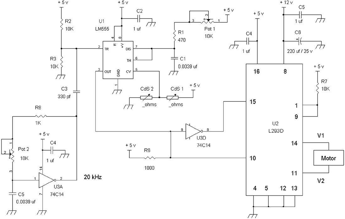
FIGURE 13.15 Motor drive with light sensors, CdS1 and CdS2.
Also, note that R6 is used as a pull-up resistor at pin 3 of the LM555 to ensure that the logic high voltage goes all the way up to 15 volts. This resistor is added because the 74C14 logic inverter requires a high-input voltage to be confirmed as a logic high signal. Standard logic inverter chips, such as the 74C04 chips, only need about 3.0 volts for logic high, whereas the Schmitt Trigger inverter chips, 74C14, require about 3.75 volts for a logic high-input signal.
In Figures 13-14 or 13-15, waveforms from pin 2 U3A (74C14 oscillator), input pin 2 of the LM555 chip with pulse narrowing (via R2, R3, and C3), output pin 3 of the LM555, and the inverted signal at input pin 15 of the L293D motor drive amplifier are shown in Figures 13-16(a) to (d) respectively.
NOTE: On the L293D chip there was an error in the 1990 and 2002 datasheets that had the motor amplifier’s power pin as pin 3 in their application notes, which is incorrect. Also the 1990 and 2002 datasheets show pin 3 in two places, which is in error. The subsequent L293D data sheets in 2004 and 2016 corrected the error and the correct motor amplifier power pin is pin 8 (as shown in Figures 13-14 and 13-15). The motor drive amplifier pin 8 has 5 volts to 30 volts, and +12 volts is typical. Pin 16 needs to be +5 volts to match the LM555’s supply voltage. So the lesson here is to double check datasheets. Sometimes a datasheet may include typos.
Also, the 20 kHz pulse frequency was chosen so that the motor could not respond to such a fast changing signal. Instead the motor’s mechanical inertia and coil inductance filter out the 20 kHz AC signal but only responds to the average DC signal from the (high frequency) pulse waveform (e.g., due to the duty cycle).
We can see that the top trace of Figure 13-16(a) shows that the 74C14 CMOS oscillator does a pretty good job in providing approximately a 50 percent duty cycle waveform whose frequency is about 20 kHz. To narrow the negative cycle (logic low) portion of this waveform capacitor, C3 along with R2 and R3 form a high-pass filter as shown in the circuits with Figures 13-14 and 13-15. The narrowed negative going pulse in the (b) waveform is in the order of about 2 μsec, which is much less than the ~ 25 μsec negative cycle (low state) of the top trace waveform (a). In this example, the pulse width is set to about a 25 percent duty cycle as shown in the (c) waveform, and the inverted (logic) signal shown in the (d) waveform has a 75 percent duty cycle. Now let’s look at how the duty cycle and average voltage works via Figures 13-17, 13-18, and 13-19.

FIGURE 13.16 Waveforms at (a) pin 2 U3A, (b) pin 2 U1, (c) pin 3 U1, and (d) pin 15 U2 of the circuit from Figures 13-14 or 13-15.
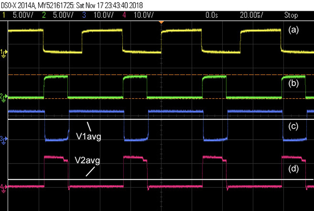
FIGURE 13.17 U3A pin 2 oscillator (a), U1 pin 3 output of LM555 (b), output at V1 pin 14 U2 (c) and its average voltage, and (d) output at V2 pin 11 U2 and its average voltage.
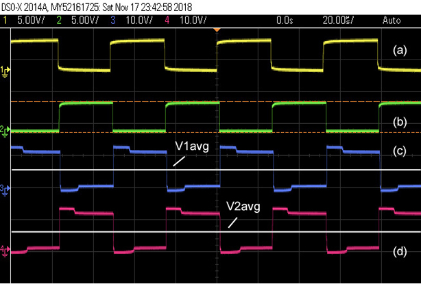
FIGURE 13.18 Top trace (a) is the oscillator signal at pin 2 of U3A, and increasing the 555’s output waveform (b) to 50 percent duty cycle causes the motor drive waveforms (c) and (d) to also have 50 percent duty cycle.
FIGURE 13.19 Top trace (a) is the oscillator signal at pin 2 of U3A, and increasing the 555’s output waveform (b) to 75 percent duty cycle causes the motor drive V1 waveform (c) to have 25 percent duty cycle with V2’s waveform (d) to have 75 percent duty cycle.
In Figure 13-17(a), the oscillator’s output is used as a reference signal. The waveform below it (b) shows the LM555’s output signal. To drive the motor, voltages V1 and V2 are applied to it, and it is the difference in average voltage (V1avg – V2avg) that determines the rotation speed and direction of the motor’s shaft. As we can see, the V1 waveform has about 75 percent duty cycle and the V2 waveform is at about 25 percent duty cycle.
Thus, the average voltages for a 12-volt supply (into pin 8 of the L293D chip) are about 12 volts × 0.75 = 9 volts = V1avg, and 12 volts × 0.25 = 3 volts = V2avg. We now have a voltage of (V1avg – V2avg) across the motor as shown in Figures 13-14 or 13-15, which is (9 – 3) volts, or 16 volts. When we change the pulse-width from the 555 chip to 50 percent duty cycle as shown in Figure 13-18(b), we see that the average voltages for V1 and V2 are the same. See Figure 13-18.
By having the 555 timer’s output waveform increased in pulse-width to 50 percent, voltages V1avg = V2avg. Thus, the voltage across the motor is (V1avg – V2avg) = 0 volts, and the rotation in the motor’s shaft is no longer turning, and thus it is stopped.
When we then increase the LM555’s pulse-width further as shown in Figure 13-19 (b), pulse-width at V1 has decreased, while V2’s pulse-width has increased. See Figures 13-19 (c) and (d), respectively. V1’s duty cycle is 25 percent so:
V1avg = 25% × 12 volts or 3 volts; and V2’s duty cycle is now
75 percent with V2avg = 75% × 12 volts or 9 volts.
The voltage across the motor is: (V1avg – V2avg) = (3 – 9) volts, or –6 volts. With the minus sign (in –6 volts), this means the DC motor’s shaft is rotating in the opposite direction.
A bridge amplifier like the L293D allows for controlling the speed and direction of the motor’s drive shaft even though, if we note, this amplifier is running off positive power supplies. That is, it does not need a negative supply to run the motor in reverse.
Note that the average voltages at V1 and V2 of U2 (L293D) or at pin 3 of U1 (LM555) can be measured with most DVMs in the range of 10 percent to 99 percent with good accuracy. The reason is because the oscillator frequency is at 20 kHz, where the DVMs tend to give an average voltage. If you suspect that a DVM is giving inaccurate readings for these measurements, you can measure the average voltage with an analog voltmeter. Again, try using an analog VOM that has at least 20,000 ohms per volt reading as to not load down the signals you are measuring.
Summary of Troubleshooting Techniques
• You can test timing circuits with LEDs to determine approximately how long the pulse is when the 555 as configured as a pulse generator (a.k.a., monostable mode).
• A loudspeaker or AM radio can be used to determine if the 555 circuit is oscillating. If the frequency is higher than what we can hear, you can connect the 555 circuit to a frequency divider (74HC393 or equivalent). Then couple a speaker amplifier to the output of the frequency divider.
• For a periodic pulse signal via the LM555, if you know the supply voltage and frequency, you can determine the pulse-width approximately by measuring the duty cycle indirectly by measuring the average voltage. You can measure the frequency of the periodic pulse signal with a DVM that has a frequency counter feature or use a frequency counter. For an approximate frequency measurement, an oscilloscope can be used.