CHAPTER 14
![]()
Troubleshooting Other Circuits, Including Kits and Projects
So far, we have seen various ways to troubleshoot mostly basic circuits, such as operational amplifiers, 555 timer chips, LEDs, and transistors. For basic troubleshooting, there are always basic techniques to look at, such as checking the supply voltages, components’ pin outs, and DC conditions. We also need to ensure that the power supply decoupling capacitors (e.g., 0.01 μf to 10 μf) have short leads and connected very close to the ICs’ power and ground pins.
In this chapter we will look at circuits that may or may not work so well. These include electronic kits such as light-sensing circuits, light transceivers (transmit and receive circuits), temperature-sensing circuits, speaker amplifiers using transistors, and IC audio power amplifiers.
Also, we will explore circuits pertaining to power supplies, microphone preamplifiers, and oscillators.
Component Kits and Test Equipment
Before we start assembling boards/kits, there are at least a few items you should have on hand. The component kits, such as assorted capacitors, resistors, transistors, LEDs, etc., can usually be purchased on the web (e.g., www.amazon.com) for less than $15 per kit. Typically, the assorted parts, such as 300 assorted red, green, blue, and white LEDs, will be about $10. Having spare parts will allow you to repair, modify, or augment the electronic circuits you experiment with. Here are the components you should have:
• Ceramic capacitor kit from 10 pf to 1 μf or more.
• Quarter-watt resistor kit, either 5 percent, 2 percent, or 1 percent values from 1Ω to 1MΩ.
• Electrolytic capacitor kit of at least 16 volts rating, but 25 working volts or more is preferable for values from 1 μf to 470 μf, although 1 μf to at least 100 μf will work fine.
• Assorted NPN and PNP transistor kits such as 2N3904, 2N3906, PN2222, and PN2907, plus any power transistors.
• If you are into radio frequency circuits, you could purchase a kit of fixed value inductors from 1 μH to at least 1000 μH.
• A basic digital multimeter (DVM), or preferably a DVM that includes a capacitance meter and a frequency counter.
• Another measuring device you can purchase for < $50 is an inductance capacitance meter. You will be able to confirm a coil’s inductance and capacitor’s capacitance value. This will be very useful should you work with radio circuits, but also with some audio circuits where large value inductors (e.g., 1 Henry coils) are used.
• A good dual-power variable voltage power supply from 0 to ± 12 volts or more, with a maximum current output of at least 500 mA. You can purchase, for example, two independent adjustable voltage power supplies and with adjustable current limiting. Setting a current limit (e.g., to < 100 mA) is desirable to avoid destroying electronic components should there be a mistake in your wiring or parts installation.
• An alternative to power supplies in most cases is to use rechargeable batteries. To prevent damage to the batteries in case of an accidental short-circuit, wire a series 0.51Ω to 2.2Ω quarter-watt resistor with the battery. This way, if there is a short-circuit, the resistor will act like a fuse and burn out.
• A simple signal generator that provides sine waves and square waves. Sine waves are often used in audio and RF circuits, while troubleshooting some digital or logic circuits will require pulse waveforms such as square-wave signals.
• Finally, if you can afford an oscilloscope, get a two-channel version of at least 25 MHz bandwidth. For example, a new 100-MHz two-channel scope (Hantek) costs around $250 US or so in 2019 on Amazon.com. For good all-around troubleshooting, a 50-MHz or 100-MHz two-channel oscilloscope will work fine.
The reason for having extra parts is that some electronic kits may come with incorrect value resistors, capacitors, or other parts. Because assorted resistors, capacitors, inductors, transistors, and LEDs are generally under $10 each, it’s a good investment to have spare parts handy. Not only can these parts be used in the electronic kit projects, but also for your own experimenting.
Of course, to build your electronic kits, you will also need a soldering pencil around 25 watts to 40 watts (e.g., a Weller SP23 or SP25 series with flat blade and conical point tips), or a soldering station that has temperature control (e.g., a Weller, Hakko, or Metcal solder station that generally costs > $100 US), solder such as 60/40 or 63/37 tin to lead composition of 0.020 inch to 0.031inch diameter with rosin flux, a pair of small long-nose pliers, a pair of small diagonal cutters, a wire stripper for various wire sizes, small screwdrivers for flat blade and Phillips screws or bolts, and wire from 18 AWG and 22 AWG, preferably some with single solid strand and stranded varieties.
LED and Sensor Kits
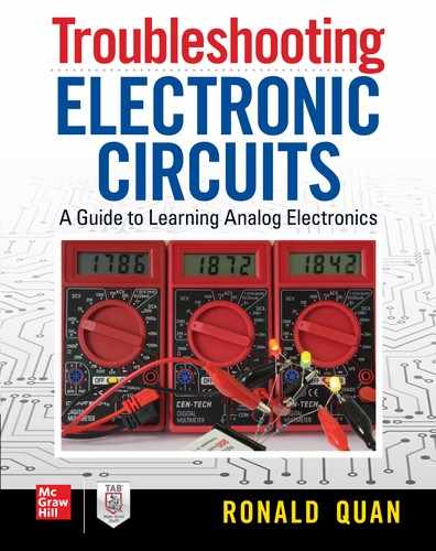
Our first electronics kit to build and test is a low power light switch that turns on in the presence of a dark room. Otherwise, with a normally lit room the switch is open circuited. This circuit uses a cadmium sulfide light-dependent resistor (LDR), which exhibits lower resistance when more light shines on it. In “total” darkness, the LDR will provide ≥ 1MΩ, while in a normally lit room the resistance will be < 10kΩ. You can test your LDR using a DVM by setting the resistance to 200kΩ (or 20kΩ). See Figure 14-1, which shows examples of two LDRs measured with DVMs. As shown on the left side where the LDR’s front side is turned toward the back wall with less light, the left side DVM shows about 6.3kΩ, whereas the LDR on the right (with its front side turned toward the light source) receives more light and measures at 2.8kΩ. Also note that the LDR on the right side shows a serpentine or zigzag pattern, which is the front side of the LDR where light is sensed.
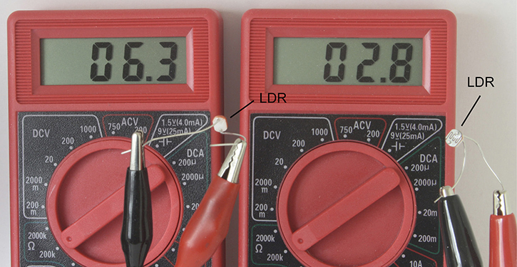
FIGURE 14.1 LDR’s resistance measurements. On the left side, the LDR is facing less light and measuring 6.3kΩ. On the right the LDR is sensing more light with a lower 2.8kΩ resistance; also note the serpentine pattern on the LDR’s front/face side. Again, the LDR is a non-polarized device, and their two leads are to be treated like the two leads of a standard resistor.
NOTE: The LDR’s two leads can be connected either way because they are not polarized.
Now let’s take a look at a DIY light sensor kit with a cadmium sulfide LDR. See Figure 14-2.

FIGURE 14.2 The light sensor kit’s unloaded board with “A” and “B” associated with the circuit shown in Figure 14-3.
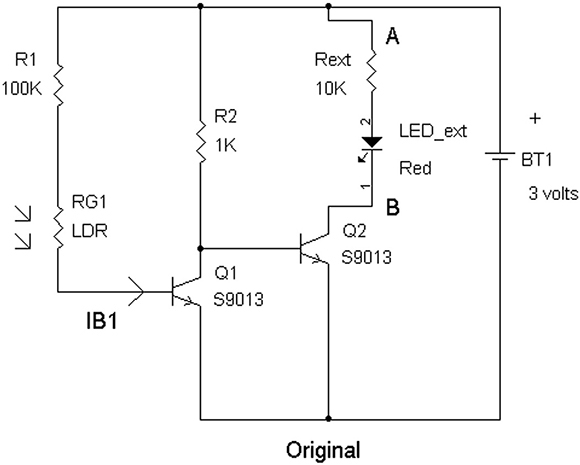
FIGURE 14.3 Schematic of the original circuit, which corresponds to Figure 14-2 with “A” and “B” terminals related to J1 OUT.
As a reference, you should take a picture of the blank printed circuit board first. This way, you have a record of where each resistor, capacitor, transistor, etc. goes. Once you load and solder in the parts, the silkscreen reference values or reference designations may be obscured. By having a picture of the blank board, you can quickly check whether you have loaded the parts in the correct locations. For example, if you loaded R2 with some value other than 1kΩ, you can refer to Figure 14-2 and confirm that R2 should be a 1kΩ. Now let’s look at the schematic in Figure 14-3.
This DIY light sensor project includes the transistors Q1 and Q2; light-dependent resistor, RG1; and resistors R1 (100kΩ) and R2 (1kΩ). Referring to the original circuit in Figure 14-3, we see that the connections “A” and “B” are used for turning on a circuit with the 3-volt supply (BT1). In this case, two AA cells in series provide the 3 volts. When light strikes the light-dependent resistor, RG1, it provides a sufficiently low resistance to provide base current, IB1, to Q1. Q1’s base current is amplified by the current gain (β1) of Q1, which is > 100, such that the voltage across the collector and emitter of Q1 is then [3 volts – (β1 IB1)R2], and wherein the lowest collector voltage is 0 volts (Note that R2 = 1kΩ.). That is, in reality, the quantity [3 volts – (β1 IB1)1kΩ] is ≥ 0 volts, but [3 volts – (β1 IB1)1kΩ] is ≤ 3 volts (or BT1).
So, when the sensor is a room that is at least normally lit (e.g., normal room light to “blazing” sunlight), RG1 has low resistance and turns on Q1 as a switch such that Q1’s collector-to-emitter voltage ~ 0 volts. Because Q1’s collector is connected to Q2’s base, this means that Q2’s base-to-emitter voltage also ~ 0 volts, which means Q2 acts like an open circuit. Therefore Q2’s collector does not draw any current and the external light-emitting diode, LED_ext, and series resistor R_ext have no current flow and LED_ext is thus not lit. However, when the light sensor circuit receives no light (e.g., light sensor module is placed in a dark room), Q1’s base current drops sufficiently low such that Q1’s collector current is low enough that Q1 is essentially an open circuit from Q1’s collector and emitter terminals. This means R2 (1kΩ) acts like a base-driving resistor to Q2’s base, which then turns on Q2 as a switch to turn on LED_ext. Thus, with sufficient base current from R2, the Q2’s collector voltage is close to 0 volts with respect to Q2’s emitter or with respect to the (–) terminal of BT1.
To troubleshoot this circuit, you can use a digital voltmeter (DVM) and connect the negative (black) test lead to the (–) terminal to BT1, and then with the DVM’s red lead measure voltages at the base and collector terminals of Q1 and then at the base and collector terminals of Q2. When in a lit room, Q1’s base voltage should be ~ 0.6 volts ± 20 percent, and Q1’s collector voltage and Q2’s base voltage should be less than 0.6 volts but no lower than 0 volts (e.g., no negative voltage reading at the collector of Q1). If the LED is not lit, you can test the sensor circuit by covering the light-dependent resistor, RG1, with your hand or place an opaque material over the RG1 that blocks out the light. If the light-dependent resistor is very sensitive (e.g., able to provide a low resistance even when there is very little light shining on it) or the Q1’s current gain is very high, you may have a harder time getting the external LED to light up in the dark.
One solution is to solder a resistor about 47kΩ (Rext_2) across the base and emitter of Q1, which should desensitize the current gain of Q1. See the #1 modified circuit with Rext_2 having a 47kΩ value in Figure 14-4. That is, RG1 now has to have a high enough resistance with R1 (100kΩ) to form a voltage divider with this extra Q1 base-to-emitter resistor Rext_2 (47kΩ) such that the voltage across Q1’s base-emitter voltage is VBEQ1 < 0.6 volt.
FIGURE 14.4 #1 modified circuit with Rext_2 = 47kΩ; and #2 modified circuit with variable/adjustable resistor POT1_ext.
For the condition that VBEQ1 < 0.6 volt, the following equation holds:
VBEQ1 = 3 volts [47kΩ/(47kΩ + R1 + RG1)]
or
VBEQ1 = 3 volts [47kΩ/(47kΩ + 100kΩ + RG1)]
We want VBEQ1 < 0.6 volt so that Q1 is off and Q2 is turned on. Suppose in a dark room, RG1 = 200kΩ, then VBEQ1 = 3 volts [47kΩ/(47kΩ + 100kΩ + 200kΩ)] which leads to:
VBEQ1 = 3 volts (47kΩ/347kΩ) or VBEQ1 = 0.4 volt
which is sufficient to turn off Q1 (e.g., collector of Q1 is an open circuit with the Q1’s emitter) and allow R1 to act as a base-driving resistor to the base of Q2. In general, the LDR is capable of having a dark (e.g., no light) resistance at least 1MΩ, which will provide an even lower than 0.4-volt VBEQ1.
We can now show a slight modification of the sensor circuit in Figure 14-4, the #2 modified circuit where we use a variable resistor (POT1_ext) across Q1’s base-emitter junction.
In Figure 14-4 with the #2 modified circuit, you can choose POT1_ext with resistance values of 20kΩ to 100kΩ. As shown, POT_ext = 100kΩ, and resistor R1 is changed from 100kΩ to 1kΩ because RG1 can vary (with light intensity) from about 1MΩ to 100Ω. So R1 = 1kΩ is used as a current limiting resistor such that if RG1 = 100Ω, RG1’s current is limited less than 3 mA. Resistor R2 is increased from 1kΩ to 3.3kΩ for increasing the sensitivity of the circuit if needed. However, the POT1 allows for a wide range of adjustments for light and dark turn-on and turn-off thresholds. Typical set values for POT1 are in the 1kΩ to 10kΩ range.
NOTE: Not every light-dependent resistor (LDR) RG1 has the same resistance per light intensity. You can generally find the data or specification sheet on the web for a specific LDR.
Figure 14-5 shows the two circuits including the modified version with a 100kΩ variable resistor (POT1 in the schematic) denoted as a potentiometer labeled as “104” on the right side.

FIGURE 14.5 The LDR sensing circuits, original and modified, with external LED indicator lamp. Notice RG1, the LDR device (with its serpentine pattern), is to the left side of Q2.
It should be noted that either LDR circuit in Figure 14-5 can have the following:
• The transistors Q1 and Q2 may be substituted with virtually any general-purpose NPN transistor with a pin out of emitter-base collector. This means a 2N3904, 2N4401, 2N4124, or MPS2222 type can be used. As long as the current gain, β, is greater than 30, the circuits will work.
• You can replace the RG1, the light-dependent resistor, with other types or sizes as long as the resistance ranges from about 100kΩ to 100Ω, from dark to bright light shining into it.
• Although the LDR circuit shown works with a 3-volt supply, it can work at higher power supply voltages up to 15 volts or more. For the modified version with POT1, make sure the series resistor is scaled accordingly for 1kΩ/3 volt supply. For example, if you use a 12-volt supply, R1 = (12 volt /3 volt) × 1kΩ or R1 → 4kΩ (e.g., either 3900Ω or 4300Ω is close enough to 4kΩ).
A Quick Detour with the LM386 Audio Power Amplifier IC
We will now look into a very popular audio power amplifier that may be used to drive a wide range of loudspeakers from the very small ones used in laptop computers to those used in “book end” speakers, for example. The commonly used LM386N-1 can deliver up to about half a watt with a 9-volt supply. Typically, this amplifier runs off batteries or a regulated power supply between 4 volts and 12 volts. It can work off a raw supply, but caution must be observed to ensure the absolute maximum 15-volt rating is not exceeded. If higher voltages are required, you can order the LM386N-4 part number that has a 22-volt absolute maximum supply rating.
When using batteries or regulated power supplies ≤ 12 volts, a circuit such as the one shown in Figure 14-6 can be used. Note all capacitors should be rated at least 25 volts.
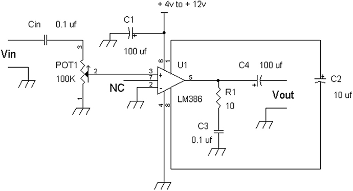
FIGURE 14.6 An example LM386 audio amplifier with battery or regulated supply with input gain control POT1. The maximum gain is 200 with C2, and 20 with C2 removed.
For battery or regulated power supply operation, pin 7 is left as a no-connect, NC, where you can optionally add an extra power supply decoupling capacitor that will be shown in Figure 14-7. One of the most important aspects of this amplifier is the series resistor-capacitor “snubbing” network R1 and C3. This snubbing network provides a resistive load at high frequencies so that the amplifier is free of oscillations should the output Vout be connected to long wires or to a loudspeaker system that represents an “unstable” or reactive load. Without R1 and C3 as configured, it is possible that the amplifier can oscillate at high frequencies. With a speaker connected, you can probe Vout with an oscilloscope to confirm no high-frequency signals are present. In general, R1 has a value between 4.7Ω and 10Ω and C3 has a range from 0.047 μf to 0.22 μf (e.g., ceramic or film capacitors ≥ 50 volts).

FIGURE 14.7 A more generalized LM386 audio amplifier circuit with decoupling capacitor C5 and feedback gain control POT2 to set the maximum gain in the range of 20 to 200.
One of the worst implementations of the snubbing network is to set R1 = 0 Ω and have Vout connected directly to C3, which will increase the chance for oscillation. Please make sure R1 is in the 4.7Ω to 10Ω range in series with C3 to ensure stable operation.
If you are using a 6-volt or 9-volt DC wall charger, chances are that it will provide DC with some ripple (e.g., hum) due to its simple rectifier and single capacitor circuit. If you are unsure how high a DC voltage the wall charger will provide, use an LM386N-4 part number and keep the wall charger’s voltage rating ≤ 12 volts. The reason is that a wall charger’s voltage under light current load can provide up to 40 percent more voltage. For example, a 12-volt DC wall charger can give up to 17 volts for its open-circuit voltage. Since the LM386N-1 is rated at 15 volts, it can be damaged by a 12-volt DC wall charger that can give out 17 volts when lightly loaded. For safety reasons, a 9-volt or 6-volt version may be a better choice to avoid damage to the LM386N-1.
The LM386 can “ignore” the hum from the power supply, providing C5 is connected to pin 7 as shown in Figure 14-7. The larger the capacitance value for C5, the lower the hum will appear at Vout. Typically, C5 = 33 μf will work fine, but larger values such as 100 μf to 470 μf will reduce hum even further.
POT2 shown as 50kΩ can actually be a value in the range of 10kΩ to 20kΩ for finer or easier control of the voltage gain. In some cases, if the maximum gain is too high at 200, which can pick up background noise in Vin, then you can lower the maximum gain to about 20 via turning/setting POT2 to 50kΩ, its maximum resistance value. See Figure 14-7.
Alternatively, you can remove C2 (33 μf) to lower the voltage gain to about 20, which would disconnect POT2 from the LM386.
Again, note that the series resistor-capacitor snubbing network, R1 and C3, is essential for ensuring that the amplifier does not oscillate at high frequencies when Vout is connected to a loudspeaker. R1 is required and should be from 4.7Ω to 10Ω, and if R1 = 0Ω, then the LM386 amplifier will likely cause oscillations at Vout.
We now will look at a light transmitter and receiver system that uses an LM386.
Photonics: A Light Transceiver System
Our next DIY kits involve a modulated light source (LED) for wirelessly transmitting audio signals to a photo-detector with playback on a loudspeaker. See Figure 14-8. The transmitter and receiver kit boards are both labeled ICSK054A on the bottom sides; and the transmitter board has provisions for two LEDs and a TO-92 transistor, while the receiver board has an 8-pin IC.
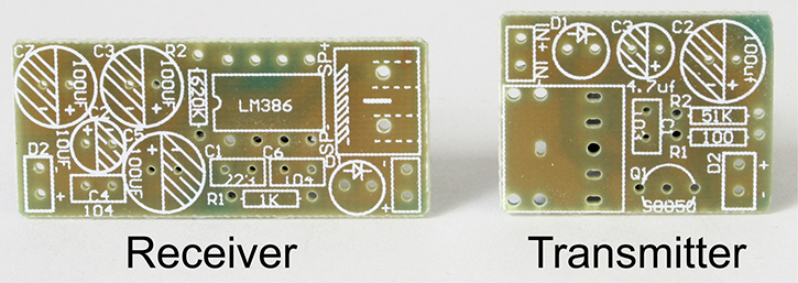
FIGURE 14.8 Light receiver board with an LM386 8-pin IC, and transmitter board with a Q1 transistor, S8050 (NPN with 1.5-amp maximum collector current).
Now let’s take a look at the transmitter’s schematic in Figure 14-9.
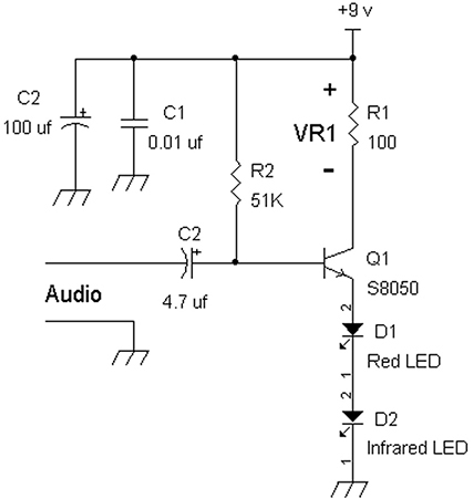
FIGURE 14.9 An emitter follower amplifier, Q1, driving two LEDs in series with an audio signal modulation (e.g., via a headphone output signal from a phone or player) via Q1’s base. With +9 volts supply and a random sample of Q1 (S8050), VR1 ~ +2.7 volts.
In Figure 14-9, the red LED, D1, works not only as a visible light emitter, but also to let you know that the LEDs, D1 and D2, are installed correctly. If D1 does not light up, you need to check the pin outs of D1 and D2. Chances are either or both D1 and D2 have been installed reversed. Resistor R1 acts as the LEDs’ current-limiting resistor, but we can use it for monitoring the LEDs’ current. By measuring the voltage across R1, VR1, as shown, the LED currents will be VR1/100Ω. For example, if VR1 = 2.7 volts, then the LED current flow through D1 and D2 will be 2.7v/100Ω or 27 mA. Also, just remember that the longer lead of an LED is the anode or (+) terminal. Q1’s DC emitter voltage is just the sum of the forward voltages across a red LED and an IR (Infrared) LED, which is about (1.8 volts +1.3 volts), respectively, or about 3.1 volts.
Now let’s take a look at the original receiver circuit as shown in Figure 14-10.
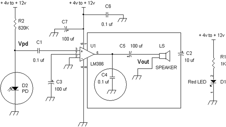
FIGURE 14.10 Original photodiode receiver design with circled problem areas.
The original design shown in Figure 14-10 needs to be modified for reliable operation. The first problem is C4 is connected directly to the output pin 5 of the LM386 amplifier, which can lead to instability or oscillations in the output signal Vout. A series resistor will be needed with C4 to correct this problem.
The second problem shown is that D2, the photodiode, is biased incorrectly from anode to cathode via R2 in forward bias mode, when in fact D2 should be biased in reverse bias mode (e.g., positive voltage at the cathode with respect to the anode). With a positive bias voltage via R2 into the anode of D2, the photodiode is conducting DC current set by R2. The DC voltage at the anode of D2 is about +0.7 volts. When a photodiode is biased incorrectly in the forward bias mode, the photodiode’s signal current is “short-circuited” back into the photodiode’s internal low resistance, which results in a very small signal at node Vpd. We can fix this problem by simply reversing the anode and cathode leads of photodiode D2 (see Figure 14-11).
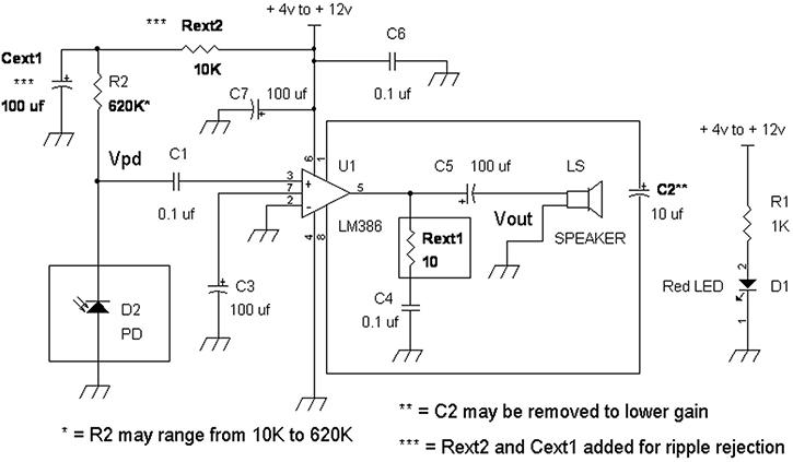
FIGURE 14.11 Modified photodiode receiver circuit to avoid oscillations by adding Rext1 and to ensure D2 (photodiode) is in the correct biasing mode. Corrections are pointed out by the rectangles surrounding D2 and Rext1.
If you happen to build the circuit as shown in Figure 14-10 (without any circuit correction to D2), you will still receive signals from Figure 14-9’s transmitter modulated light signals, but the speaker’s (LS) volume will be low.
Figure 14-11 shows the circuit corrections, which are shown inside the rectangular outlines. As shown, we see now that the photodiode, D2, is reversed in connection such that a positive voltage is provided to the cathode. Depending on the light shining on the photodiode, the DC voltage at D2 is [Vsupply – (Ipd × R2)].
For example, if the supply voltage is 6 volts and the photodiode current is 1 μA with R2 = 620kΩ, the D2 cathode voltage is 6 v – 1μA × 620kΩ = (6 volts – 0.62 volt), or +5.38 volts at D2’s cathode. Resistor R2 also sets the receiver gain since it is a load resistor for the photodiode current received by D2. For lower gain, R2 can be set to about 10kΩ, and for maximum gain R2 can be 620kΩ, the original value. Note that the input resistance of the LM386 is already 50kΩ, which is in parallel with R2 AC signal-wise.
Rext2 and Cext1 are optional if the power supply is from a wall charger whose DC voltage includes ripple or hum. Otherwise, you can remove Cext1, and set Rext2 = 0Ω as a wire.
You will get the furthest range between the transmitter and receiver with the component values shown in Figure 14-9 and Figure 14-11. The modified photodiode receiver in Figure 14-11 is very sensitive and will pick up the flickering from room lights and produce hum or buzzing noise. If you turn off the lights, the buzzing noise will be reduced dramatically. Also, if the photodiode receiver is playing too loud for comfort, you can reduce the audio gain tenfold by removing C2, or alternatively reduce the sensitivity even further by having R2 = 4700Ω.
The correct pin out for the photodiode D2 is shown in Figure 14-12, which includes a photo of the transmitter and receiver with loudspeaker. Again, the transmitter’s input jack will accept line-level audio signals from a phone, digital player, or radio. Signals from a microphone are too small in amplitude and will require a preamplifier with a gain typically between 30 (electret microphone) and 300 (dynamic microphone) depending on the type of microphone.

FIGURE 14.12 Photodiode D2’s correct pin outs as soldered to the receiver board.
See Figure 14-13, which shows examples of microphone preamplifiers that amplify signals from microphones to about the same level that comes from a digital player or radio.
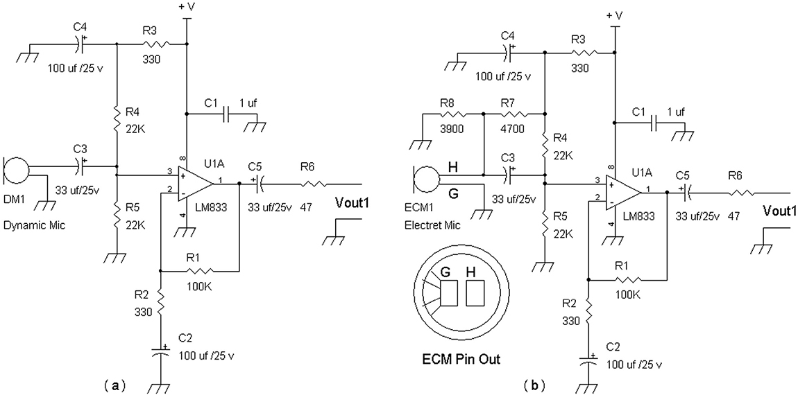
FIGURE 14.13 (a) Preamplifier circuits for dynamic microphones and (b) for electret condenser microphones (ECM). The power supply may range from 7.2 volts to 15 volts for +V.
For a dynamic microphone, usually a (voltage) gain of about 50 dB or 300 is required; that is shown in Figure 14-13 (a) where the feedback resistors R1 and R2 set the gain at (1 + R1/R2) or the gain is (1 + 100K/330) ~ 304. A dynamic microphone usually wants to be loaded with ≥ 1kΩ resistance, which is R4 || R5 = 11kΩ due to having two 22kΩ resistors in parallel. Note that R3 to C4 is an AC short-circuit to ground due to its large capacitance (100 μf). To remove noise from the power supply line, +V, R3 and C4 form a low-pass filter at about 5 Hz. This means if +V has some 50 Hz or 60 Hz ripple voltage, it will be attenuated by about tenfold or more at the plus terminal of C4. Having a low-noise DC bias voltage is essential for microphone amplifiers. If more filtering is required, C4 should increase to 1000 μf, if necessary, to provide low noise at Vout1.
Figure 14-13 (b) shows an electret condenser microphone preamplifier. Electret microphone capsules that are commonly used in DIY kits have an identifying ground lead as shown in the ECM Pin Out diagram. Most electret microphone capsules have a ground or shield lead, G, and a hot or + lead denoted by H. When you view the electret microphone’s bottom side, you will see that the canister or metal body is connected to the ground terminal, G, via traces to the outer ring or case. See the illustration that is shaded in gray. Since the output from an electret microphone is typically 10× more than the dynamic microphone, the preamplifier’s gain is set to about 31 via R1 = 10kΩ and R2 = 330Ω. The gain is then (1 + R1/R2) = (1 + 10K/330) ~ 31. To bias the electret microphone, it requires an equivalent 1000Ω to 2200Ω load resistor with a bias voltage from 3 volts to 9 volts max. Generally, a 3-volt bias is common.
For Figure 14-13 (b), the voltage at C4’s plus terminal is still about +V due to a very small low current flowing through R4 and R5 that incurs a small voltage drop across R3.
If +V = 9 volts, then the voltage at the junction of R8 and R7 is:
9 volts × [R8/(R7 + R8)] or 9 volts × [3900/(4700 + 3900)] = 4.08 volts. The equivalent load bias resistor to ECM1 is R7 || R8 or 3900Ω || 4700Ω = 2131Ω. Resistors R4 and R5 are 22kΩ that present an extra 11kΩ AC signal load to the microphone. However, we can make R4 = R5 = 220kΩ to provide a negligible loading to the electret microphone, but should be aware that the DC bias voltage will take about 10 seconds to settle down or stabilize due to the time constant with C3, which is:
τ = C3 × [R4 || R5] with C3 = 33 μf and due to R4 || R5 = 220kΩ || 220kΩ or R4 || R5 = 110kΩ so τ = 33 μf × 110kΩ = 3.6 seconds.
Normally it takes about three time constants for the circuit to settle, which is then 3 τ = 3 (3.6 sec) = 10.8 seconds.
One other thing to notice is that the values for R7 and R8 were chosen to be unequal with resistors R8 < R7 to have less than half the supply voltage at C3’s negative terminal. This is done so that electrolytic capacitor C3 is DC biased correctly. The reason is so that the DC voltage at the negative terminal of C3 is guaranteed to be less than the DC voltage at the positive terminal of C3 where the resistors R4 and R5 are equal to provide about 50 percent of +V.
Thermal Sensing Circuit via Thermistor (Temperature-Dependent Resistor)
This DIY project uses a thermistor that looks almost like a ceramic capacitor. See Figure 14-14. However, it is a resistor that changes resistance values with temperature. There are two types of thermistors, one with a negative temperature coefficient and the other with a positive temperature coefficient. The negative temperature coefficient (NTC) version has reduced resistance when heated up, and increased resistance when cooled. And the positive temperature coefficient (PTC) thermistor has increased resistance when heated, and decreased resistance when cooled. For this project, we will be using the negative temperature coefficient version that has lower resistance when the temperature is raised.
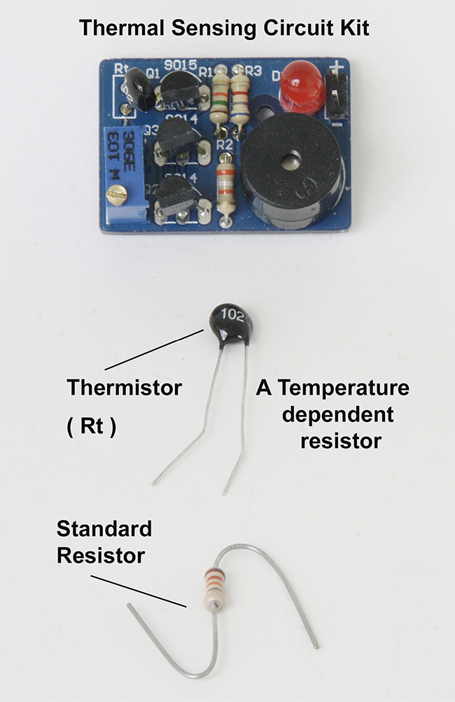
FIGURE 14.14 Sensing circuit (top), thermistor (middle), and resistor (bottom).
The DIY circuit also includes a multiple-turn potentiometer. See Figure 14-15.

FIGURE 14.15 A single-turn potentiometer on the left and a multiple-turn version on the right. The single turn potentiometer allows setting the mid-resistance point by observing the slit’s reference position above the “103” for 10kΩ, whereas the multi-turn potentiometer has no such reference position on its adjustment.
Now let’s take a look at the original DIY circuit in Figure 14-16.
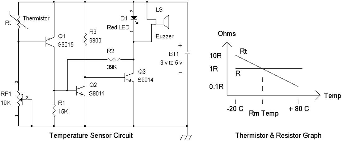
FIGURE 14.16 Temperature sensor circuit with a graph of an example of the thermistor’s resistance, Rt, and an ideal resistor, R, plotted in terms of temperature versus resistance. The graph shows a negative temperature coefficient (NTC) characteristic for Rt, the thermistor.
Let’s start with the Themistor & Resistor Graph first, which shows for an ideal resistor, R, whose resistance does not change with temperature. However, a negative temperature coefficient (NTC) thermistor, Rt, in the graph shows higher resistance at cold temperatures and lower resistances at hot temperatures. This graph is an approximation of an NTC thermistor, part number TTC05102 made by TKS. In this example let’s start out at room temperature, 25 degrees C, Rt = 1000Ω. When we look at the graph, this means at a very cold –20 degrees C, the resistance is tenfold greater or Rt = 10 × 1000Ω = 10kΩ, and at a very hot +80 degrees C, the resistance is at 10 percent of the room temperature resistance or Rt = 0.1 × 1000Ω = 100Ω. A way to test a thermistor is to connect it to an ohm meter (DVM) and observe that the resistance will change when you heat the thermistor by just holding it with a finger and thumb. For example, if you take the 1000Ω thermistor (e.g., marked 102) from the DIY kit before soldering it to the board, measure it first. Set the DVM to the 2000-ohm setting and observe the resistance before placing your hand on it. As you raise the thermistor’s temperature with your finger and thumb, the thermistor’s resistance should drop slightly.
The circuit in Figure 14-16 has a voltage divider formed by Rt and variable resistor RP1. RP1 is set first to light up the LED, and then RP1 is adjusted again until the LED just turns off. When the LED just turns off this means Q3 is turned off because the base-emitter voltage at Q3 is close to 0 volts due to Q2 being turned on. Q2 acts as an inverting logic gate with the base as the input and collector via load resistor R3 as the output. With Q2 turned on, this means there is sufficient base current drive via Q1’s collector so that the collector-to-emitter voltage of Q2 is close to zero volts. With Q1’s collector supplying current to the base of Q2, this means that the voltage divider with RP1 and Rt forms about 0.6 volt at the emitter-base junction of PNP transistor Q1. When thermistor Rt warms up, its resistance drops and the voltage across Q1’s emitter-base junction voltage drops below the 0.6-volt turn-on voltage for Q1, which means there is no collector current flowing into Q2’s base. When this happens Q2 is at cut-off, and there is no Q2 collector current, which means R3 now supplies base current to Q3 and provides about 0.6 volt at the base-emitter junction of Q3. With Q3 turned on, Q3’s collector current sinks current and turns on the LED. The speaker/buzzer, LS, is connected across the LED, which provides about 1.8 volts via the LED to LS that is supposed to turn it on for providing a noticeable alerting sound. When the thermistor Rt cools down, its resistance increases sufficiently to provide an emitter-to-base voltage to Q1 such that Q1’s collector current is provided to Q2, which then turns on Q2’s collector-to-emitter junction and provides, via R3, a logic low voltage to the base-emitter voltage of Q3 so that the LED and buzzer are turned off due to Q3 being at cut-off.
NOTE: An intuitive way of figuring out Figure 14-16 is to “pretend” that at low temperatures, Rt = open circuit, or Rt can be thought of as removed from the circuit; and at high temperatures, Rt = 0Ω or Rt is a short-circuit. Often, you can quickly analyze a circuit by looking at the two extremes of a particular parameter (e.g., resistance). In this case it is Rt’s resistance range. When Rt is an open circuit = infinite ohms, Q1 will turn on via pulling base current via RP1, and Q1 will supply collector current to Q2’s base. And when Rt = 0Ω, this means the emitter-base junction of Q1 is shorted out to zero volts. This puts Q1 in the cut-off mode, and there will be no collector current from Q1 flowing into Q2’s base, which causes Q2 to be in cut-off as if Q2’s collector was disconnected to R3 and to the base of Q3. With Q2’s collector disconnected, we then have R3 via the supply voltage providing base current to Q3, which then turns on the LED and speaker/buzzer.
So, does the circuit in Figure 14-16 looks like a workable design? Yes and no. There are a few problems. One is that if the adjustable resistor RP1 is accidentally set to zero ohms or close to zero ohms such as 10Ω, you may end up with burnt-out parts for Q1, Q2, and RP1. Also, the other problem is that the LED’s maximum current may be exceeded via Q3’s collector current because there is no reliable current-limiting mechanism. Q3’s collector current is set by the base drive resistor R3. For example, if we have BT1 = 5 volts, then the base current into Q3 is about (5 volts – VBEQ3)/6800Ω = (5 V – 0.7 V)/6800Ω or 632 μA.
Q3’s collector current is β × 632 μA. If we have Q3’s current gain β = 100 then Q3’s collector current is 100 × 632 μA or 63 mA, which is excessive for driving LEDs (e.g., LEDs generally operate at 1 mA to 20 mA). Third, the buzzer really requires about 3 volts or more to produce sufficient volume. The LED, D1, supplies only about 2 volts to the speaker/buzzer, LS, which sounded very soft. See Figure 14-17.
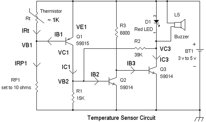
FIGURE 14.17 When RP1 is adjusted to 10Ω, Q1, Q2 and RP1 itself may be damaged due to excessive current or power dissipation that leads to burnt-out components.
Now let’s take a look at Figure 14-18, which substitutes a diode and resistor to show the excessive currents and power dissipation.
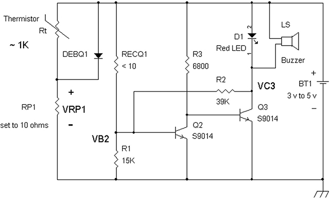
FIGURE 14.18 Excessive current via diode DEBQ1 (equivalent diode representation of the emitter-base junction of Q1) and resistor RECQ1 (an example emitter-to-collector resistance of Q1) when RP1 is set to 10Ω.
In Figure 14-18 if the supply voltage is 5 volts, then the voltage across RP1 set to 10Ω is VRP1 = (5 volts – 0.7 volt) = 4.3 volts. The 0.7 volt is due to the turn-on voltage across the emitter-base junction diode (Q1 of Figure 14-17) connection as being represented by DEBQ1. Most variable resistors or potentiometers have a 250 mW or 500 mW rating. With 4.3 volts across RP1 = 10Ω, the power dissipated into RP1 = [(4.3)2/10] = [18.49/10] watts or 1.849 watts that can burn out RP1 that is set to 10Ω. The current through DEBQ1 is VRP1/10Ω or 4.3 volts/10Ω = 430 mA. The maximum (base or collector) current rating for both S9015 and S9014 is about 100 mA. This means Q1 may burn out. And when we look at the base current into Q2, it is similar at (5 volts – VBEQ2)/RECQ1 ~ (4.3 volts/10Ω) ~ 430 mA, where VBEQ2 ~ 0.7 volt. Therefore, Q2 is running at excessive current and it too may burn out.
To ensure a safe and reliable circuit that reduces any chance of burning out RP1, Q1, and Q2, we need to add current limiting resistors.
See Figure 14-19 that shows one such example solution as highlighted in rectangles around resistors Rext1, Rext2, and Rext3. Resistors Rext1 and Rext2 protect RP1, Q1 and Q2, while Rext3 protects D1 (Red LED) from over-current. When D1, the LED, is turned on, via Q3 being turned on, and with Q3 acting like a switch such that the collector is effectively grounded, the LED current is limited by (BT1 – VLED)/Rext3. This leads to the LED current as: (5 volts – 1.8 volts)/220Ω or (3.2 volts/220Ω) = 14.5 mA = LED current. See the circuit in Figure 14-19 for a reference to the text on this page.
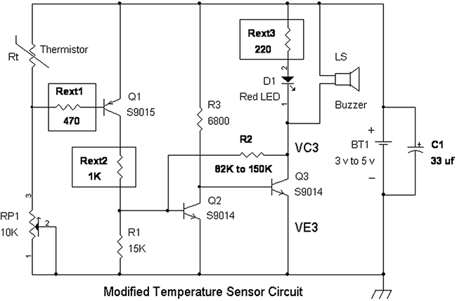
FIGURE 14.19 Current-limiting resistors Rext1, Rext2, and Rext3, which prevent damage to D1, the red LED, and transistors Q1 and Q2. C1 is added to reduce noise in the supply line.
Again, Rext3 also allows Q3 to saturate and act like a switch when R3 supplies current to its base terminal. With Q3 in saturation, the collector voltage, VC3, is nearly the emitter voltage, VE3, which is the ground voltage.
It should be noted that the resistor values for Rext1, Rext2, and Rext3 can be other values typically in the range of 220Ω to 1000Ω. For example, you can make all of these resistors 220Ω. What to be cautious of is to not make Rext1 or Rext2 too large of a value such as 470kΩ, which will render the circuit inoperable. For example, if Rext2 = 470kΩ, there is no way that Q2 will turn on when Q1’s collector is turned on to +5 volts. This is because the voltage at the base of Q2 will be +5volts [R1/(R1 + Rext2)] = +5 volts [15K/(15K + 470K)] = 0.154 volt, which is less than the required + 0.6 volt to turn on Q2’s base-emitter junction.
Resistor R2 is a positive feedback resistor from Q2’s input base to Q3’s output collector. Recall that each grounded common emitter amplifier has an inverting property in terms of phase from input to output. When you cascade two inverting amplifiers or two inverted logic gates, the result is an in-phase output signal from the collector of Q3 referenced to an input signal to the base of Q2. R2 serves the purpose of slightly biasing the base of Q1 when Q3 is off. There is some slight leakage current via D1 and Rext3 into R2 at the collector of Q3 to the base of Q1. R1 forms a voltage divider circuit with R2. If R2 is too low in value, then the circuit can latch up because R2 will provide a sufficiently high logic voltage to the base of Q2 such that Q2 is turned on and Q2’s collector will output a logic low. This will cause Q3 to turn off all the time because there is no way now to lower the voltage at Q2’s base to a logic low since Q1’s collector current can only add or increase voltage to the input base of Q2. Typically, you can measure the base voltage with a DVM and select a value for R2 such that it is in the 0.10-volt to 0.4-volt range when Q3 is turned off. When the supply voltage is increased, R2 should be increased as well (e.g., such as proportionally). For example, in Figure 14-19, the 82kΩ value was chosen for a 4-volt supply. If we increase to 5 volts, then R2 = [5 volts/4volts] × 82kΩ or R2 = 102.5kΩ ~ 100kΩ.
However, the real reason for R2 is to provide a hysteresis effect on the temperature sensor. By having hysteresis, this means that the circuit acts like a thermostat in the way the LED/buzzer is turned on and off due to temperature. That is, the trip points for turn on and turn off are at different temperatures so as to avoid chatter or flickering in the LED. The turn on will be at one temperature, but the turn off will be at another temperature many degrees lower. For example, if the sensor is set to light the LED at +27 degrees C, it will not turn off until the temperature is lower, such as at +22 degrees C.
Finally, on this sensor, there are other ways to add the current-limiting resistors. For example (but not shown here), in pins 1 and 2 of RP1 that are connected to ground, we can break the ground connection and place a 470Ω series resistor connected to ground and to pins 1 and 2 of RP1. These modifications (Rext1, Rext2, and Rext3) as shown in Figure 14-19 can be done easily on the printed circuit board (e.g., without cutting printed circuit board traces). We only need to lift the base and collector leads of Q1 and solder one lead of Rext1 and Rext2 to the traces, while soldering the other ends of Rext1 and Rext2 to the base and collector leads of Q1. The same approach was made to the D1 LED, where either cathode or anode lead can be lifted with one lead of Rext3 soldered to the printed circuit board, and the other lead of Rext3 soldered to the LED. See Figure 14-20 for a close-up photo.
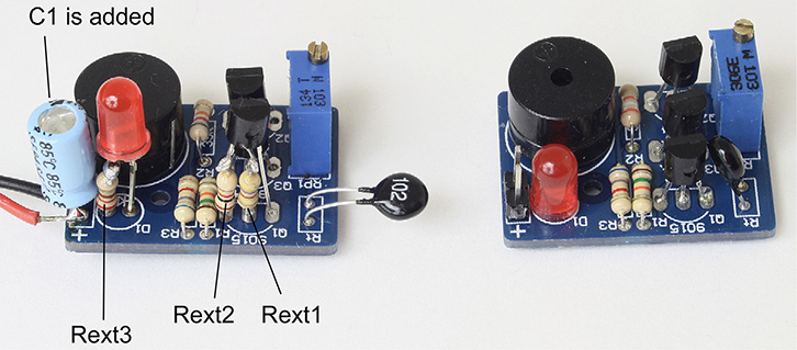
FIGURE 14.20 The modified version on the left side and the original circuit on the right side. The large round device is the speaker/buzzer.
In Figure 14-20 (left side), it was found that separating the thermistor, Rt, from Q1 worked better in terms of testing it. For example, if you heat both the thermistor (Rt) and Q1, the sensing effect slightly cancels out each other. Also, a decoupling capacitor is added across the supply line because when the speaker sounds off, some noise is added to the supply line. A 33-μf decoupling capacitor (C1) reduced this noise. See Figure 14-20 (left side) for the added C1.
The speaker/buzzer, LS, is a piezo speaker that has infinite DC resistance, but provides a tone similar to the one from a smoke alarm when activated with a DC voltage across it. Note: The speaker buzzer is polarity sensitive and must be installed correctly (see Figure 14-21).
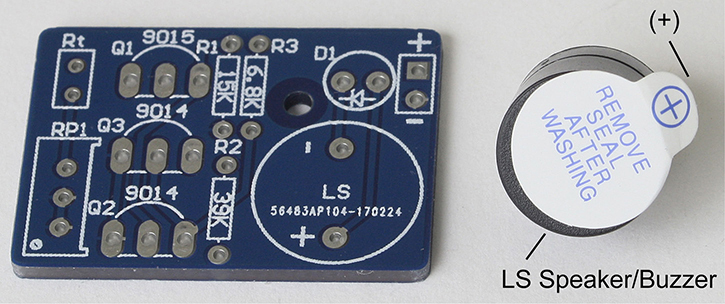
FIGURE 14.21 The speaker/buzzer in this DIY circuit is polarized and must be installed according to LS (–) and (+) pin outs in the board’s silkscreen marking. The LS speaker/buzzer is shown on the right side with the identified positive (+) terminal.
If the speaker/buzzer, LS, is installed backwards, it will not produce the alarm tone. This device is really not a speaker in the usual sense, but instead a tone buzzer that requires DC to operate it.
A Circuit Using an Electrolytic Capacitor Incorrectly
Here’s a strange audio amplifier circuit at first glance that has a reverse biased electrolytic capacitor to include a leaky internal resistive load to a transistor’s collector terminal. This amplifier was used with a single IC (e.g., MK484 or TA7642) AM radio kit. See Figure 14-22. Adjusting the volume is done with potentiometer, P1.
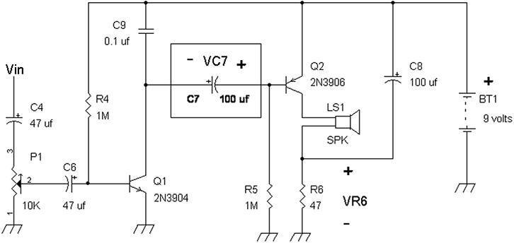
FIGURE 14.22 An audio amplifier with no apparent DC path for Q1’s collector because of capacitors C9 and C7 apparently blocking DC current flow.
This circuit actually works with a polarized electrolytic capacitor C7 (highlighted within the rectangle) because C7 is incorrectly reverse biased, and C7 will then include a leaky internal resistor in parallel with it. Reverse biasing C7 is strongly not recommended because it can be unsafe. If not for the collector of Q1 to limit the current flow of C7, this circuit can cause C7 to be damaged. As configured, the voltage across the 47Ω resistor, R6 = VR6 ~ 7 volts DC. The 7 volts is actually bad because there is almost 1 watt of power dissipation across R6, a quarter-watt resistor. Recall that power, PR6 = [V2/R] = 72/47Ω = (49/47) watt ~ 1 watt. Worse yet, the collector current of Q2 = ICQ2 is also the current flowing into R6, which is 7 volts/47Ω ~ or ICQ2 = 149 mA. Q2, a 2N3906, has a maximum collector current rating of 200 mA. Normally you try to run your transistors at < 50 percent max collector current for reliability reasons.
And if we look at Q2’s power dissipation, PQ2 = VECQ2 × ICQ2. To find VECQ2, we need to find Q2’s emitter voltage, which is BT1 = 9 volts, and also Q2’s collector voltage, VCQ2 = collector current ICQ2 × (resistance of LS1 + R6). If LS1 is an 8Ω speaker, then VCQ2 = 149 mA × (8Ω + 47Ω) = 8.19 volts. VECQ2 = VEQ2 – VCQ2 = 9 volts – 8.19 volts or VECQ2 = 0.81 volt and thus, PQ2 = VECQ2 × ICQ2 or PQ2 = 0.81 volt × 149 mA = 120 mW = PQ2. However, Q2’s maximum power dissipation is about 200 mW, so again we are running the transistor hot.
If we take into consideration battery life from BT1, a 9-volt battery with about 200 mAH rating, Q2 is draining in the order of 149 mA. This means about 1 hour of usage before the battery is exhausted. So, although Figure 14-22’s circuit works as an audio speaker amplifier, it will drain the battery too quickly, not to also mention that it’s dangerous to have electrolytic capacitor C7 put in backwards (i.e., unsafe when C7 is incorrectly biased or reversed biased).
Now let’s look at Figure 14-23. It shows an equivalent circuit, including an internal resistor to C7.
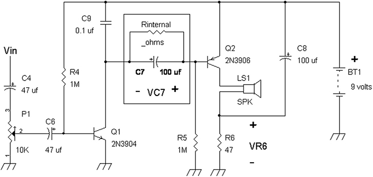
FIGURE 14.23 A reverse biased electrolytic capacitor C7 can be approximated with an internal resistor, Rinternal, as shown here. Potentiometer P1 adjusts for volume.
With C7’s equivalent internal or built-in resistor, Rinternal, in parallel with C7, we can now see that from Q2’s base, DC current flows to Q1’s collector. In essence, Rinternal is now an equivalent load resistor for Q1. Various standard 100-μf electrolytic capacitors were tried in this circuit and VR6 measured around 7 volts. However, when three 33-μf capacitors were paralleled (to equal ~ 100 μf) and placed into the circuit as C7, VR6 dropped to 1.5 volts. This means that Q2’s collector current cannot be reliably set by the reverse biased leakage resistance, Rinternal.
Also keep in mind that there are many different types of electrolytic capacitors, including low leakage ones that will vary Q2’s collector current. For example, if C7 is a very low leakage electrolytic capacitor, even when reverse biased, this means that Q1’s and Q2’s collector currents may be “starved” and thus the amplifier will deliver insufficient signal current to the loudspeaker. We can do an initial fix to this circuit via Figure 14-24.
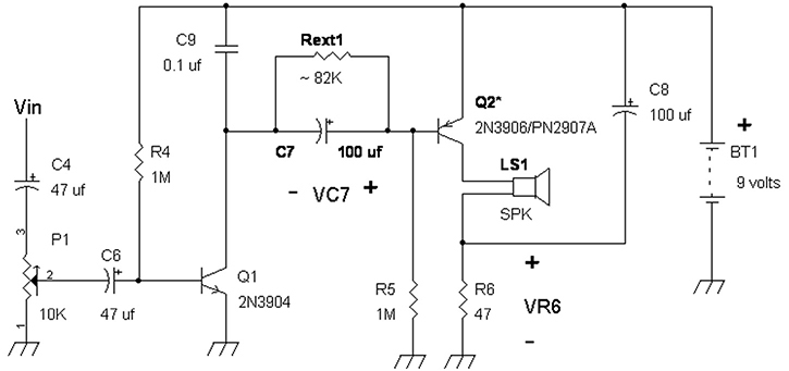
FIGURE 14.24 C7 is installed correctly and external biasing resistor Rext1 is added as shown. Potentiometer P1 adjusts for volume.
When an electrolytic capacitor (in Figure 14-24) is connected correctly polarity-wise, the internal leakage resistance goes up to near infinite ohms. So, the electrolytic capacitor, biased properly, truly blocks DC current. So, if C7 is connected correctly and without an external resistor in parallel with it, Q1 will have no load resistor and its collector current goes to zero.
Also notice that Q2 can be upgraded in terms of maximum collector current and power dissipation by choosing it as a PN2907A, which has 600 mA collector current and 600 mW power ratings as compared to the 200 mA and 200 mW ratings of the 2N3906.
In Figure 14-24 the external biasing resistor Rext1 in parallel with the correctly installed C7 (positive terminal of C7 connected to Q2’s base), we provide a load resistor for Q1’s collector, and we can set Q2’s collector current. For example, if Rext1 = 82kΩ for a particular set of Q1 and Q2 transistors, then the voltage across R6, which is VR6 = 2.01 volts. This means Q2’s collector current is (2.01 volts/R6) = 2.01 volts/47Ω or 42.7 mA, which gave sufficient speaker volume with the IC radio using the MK484 or TA7642. Given the much lower current from 149 mA originally, at least the battery will last almost four times longer. In another example, when Rext1 → 56kΩ, VR6 → 2.85 volts or Q2’s collector current → 60.6 mA (2.85 volt/47Ω = 60.6 mA). The drawback to this circuit is that Rext1 in Figure 14-24 needs to be selected accordingly because Q1 and Q2 have a wide range of current gain (β) variation (e.g., 2:1 of β variation) that will affect Q2’s final DC collector current.
However, we can modify this circuit to be insensitive to the transistors’ current gain β with the negative feedback amplifier circuit shown in Figure 14-25.
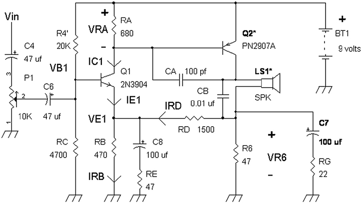
FIGURE 14.25 A feedback amplifier circuit for a more reliable Q2 DC collector current setting. Potentiometer P1 is used for adjusting volume. R6 (47Ω) is rated at 1 watt.
Let’s look at Figure 14-25 first in terms of DC conditions. We treat the capacitors as open circuits or infinite DC resistance devices (e.g., you can imagine all capacitors to be removed for DC analysis). This is a current sensing amplifier with R6 as the sense resistor. Whatever the voltage across R6 is determines Q2’s collector current, which in turn determines the drive current into the loudspeaker LS1. To provide adequate loudness from the speaker, we generally need something in the range of 10 mW to 50 mW. For example, some of the earliest simple two or three transistor radios in the 1960s typically had about 50 mW of audio power, which played loudly with its 2.25-inch speaker. For adequate playing volume, having at least 10 mW will suffice with a reasonably efficient speaker such as a 2.25-inch to 4-inch 8Ω speaker.
For the analysis with C7 or RG removed, the power into the speaker from this amplifier is about 0.5 (ICQ2)2 × Rspeaker, where ICQ2 = Q2’s collector DC current and Rspeaker is the LS1 loudspeaker’s impedance that is typically 8Ω. For example, if we set VR6 = 2.5 volts, then ICQ2 = 2.5 volts/47Ω or ICQ2 = 53 mA. The audio power output is then P = 0.5 (ICQ2)2 × Rspeaker or 0.5 (0.053Amp)2 × 8Ω = 22.6 mW. As we can see, just having a higher-impedance speaker proportionally increases the power via P = 0.5 (ICQ2)2 × Rspeaker. For example, given the same conditions of 53 mA, if we use a 16Ω speaker instead of the 8Ω version, then the power to the speaker is increased twofold to 2 × 22.6 mW or 45.2 mW. And if we choose a 45Ω speaker, then the power output will be 0.5 (0.053Amp)2 × 45Ω = 127 mW.
Figure 14-25 shows a two-transistor common emitter amplifier for both stages Q1 and Q2. It actually looks sort of like an op amp with the output at Q2’s collector, the non-inverting input at the base of Q1, and the inverting input at the emitter of Q1. The DC feedback elements are resistors RD and RB. To understand how this circuit works, we need to look at the DC currents flowing through Q1’s emitter, IE1, with current flowing through RD via IRD, and current flowing through RB, IRB. We will need to balance all the currents accordingly so that Q1’s emitter current plus the current from RD via VR6 equals the current flowing through RB. Put in another way we can say that IRD + IE1 = IRB. Also, in order to make this circuit work properly in terms of output current swing into the loudspeaker (SKR), the voltage VR6 across R6 must be greater than Q1’s emitter voltage referenced to ground.
Q1’s base voltage, VB1, is set by the voltage divider circuit R4' and RC, which is: 9 volts × [RC/(R4' + RC)] = 9 volts × [4700/(20,000 + 4700)] or 1.71 volts. We can approximate that Q1’s base-to-emitter voltage VBEQ1 = 0.7 volts, so Q1’s emitter voltage is Q1’s base voltage minus Q1’s base-to-emitter voltage. Q1’s emitter voltage = (1.71 volts – 0.7 volt) or Q1’s emitter voltage VE1 ~ 1 volt. The current (IRB) flowing through RB = 470Ω, then Q1’s emitter voltage is divided by 470Ω or IRB = 2.12 mA.
Generally, we can ignore Q2’s base current adding to Q1’s collector current. And make the approximation that the collector current of Q1 related to the voltage across RA, which is the VEB turn-on voltage of Q2 of about 0.7 volt. Q1’s collector current is VEB/RA = 0.7 volt/RA or Q1’s collector current = 0.7 volt/ 680Ω or IC1 ~ 1 mA. Since the collector and emitter currents are generally the same, IC1 = IE1 for large current gain β for Q1, and we also have IE1 = 1 mA.
This means Q1’s emitter current IE1 ~ 1 mA since the collector current and emitter currents are approximately equal when the transistor is operating as an amplifier.
If we want the voltage across R6, VR6 set to 2.5 volts, then the current flowing through RD is: IRD = (VR6 – Q1’s emitter voltage)/RD or (2.5 volts – 1 volt)/RD or IRD = 1.5 volts/RD. Now let’s put everything together.
Since IE1 + IRD = IRB (and equivalently IRD = IRB – IE1), and with IE1 = 1 mA, IRD = 1.5 volts/RD and IRB = 2.12 mA we have:
1 mA + 1.5 volts/RD = 2.12 mA
Or put in another way by subtracting 1 mA from both sides:
1.5 volts/RD = 1.12 mA, which leads to RD = 1.5 volts /1.12 mA = 1.34kΩ, or RD = 1340Ω. Again please refer to Figure 14-25.
With RD → 1.5kΩ, VR6 will be a little bit higher than 2.5 volts as originally set. We can find VR6 via the following, which you may skip because of the equations.
The current flow through RD is (VR6 – VE1)/RD = IRD. But from the previous equation we know that IRD = IRB – IE1 and that IRB = 2.12 mA and IE1 = 1 mA. So, this leads to IRD = 2.12 mA – 1 mA or IRD = 1.12 mA. Now we can find VR6 by (VR6 – VE1)/RD = IRD = 1.12 mA. Since VE1 ~ 1 volt and RD → 1.5kΩ we have: (VR6 – 1 volt)/1.5kΩ = 1.12 mA or equivalently:
(VR6 – 1 volt) = 1.12 mA × 1.5kΩ or (VR6 – 1 volt) = 1.68 volts, which leads to: VR6 = 1.68 volts + 1 volt or VR6 = 2.68 volts.
Although this analysis is a bit long-winded, it accurately predicts what VR6 will be. But when making an approximation, it’s just easier to build the circuit and measure VR6 when there is no audio input signal present.
To get an approximation of the AC gain, G, from the base of Q1 to VR6, it is with C8 taken as an AC short-circuit at typical audio frequency from 100 Hz and up, and with RD = 1500Ω, RB = 470Ω and RE = 47Ω and (RB || RE) = (470Ω || 47Ω) ~ 42Ω:
G = {1 + [RD/( RB || RE)]}
For this example, G = [1 + (1500Ω/42Ω)] ~ 36.
Finally, to ensure that this amplifier does not oscillate, capacitors CA and CB are added. The loudspeaker LS1 can be modeled as a resistor in series with an inductor. The inductive part of the LS1 comes from its voice coil winding. Capacitor CB is connected in parallel with the speaker to act like an AC short-circuit at higher frequencies and thus “short” out the inductive portion of the loudspeaker. Capacitor CB also provides an AC path at high frequencies to the current sense resistor R6 that is grounded. With Q2’s collector coupled to R6 via CB at higher frequencies, capacitor CA is used as a compensation capacitor that ensures the amplifier works without causing oscillation or peaking high-frequency response. When swept from 100 Hz to 100 kHz at the input terminal, Vin, the output at VR6 responded flat to about 50 kHz before rolling off at frequencies above 50 kHz. Capacitor CB actually may have a capacitance range from 0.01 μf to 0.1 μf.
Identifying and Fixing “Bad” Circuit Designs
When I was starting out in electronics, there were many projects from hobbyist magazines and books. Most of these worked, but a few got my head scratching. Some circuits would not work, and I went for help to my nearby TV repair shop.
Here’s one example of a variable DC power supply shown in Figure 14-26.

FIGURE 14.26 A DC power supply circuit from a hobbyist book from the 1960s. This circuit does not work well. (The original schematic labeled R1 as a potentiometer.)
The circuit uses a 24-volt AC secondary winding transformer, T1, that delivers 24 volts RMS AC to a full-wave bridge rectifier from diodes D1, D2, D3, and D4. At the cathodes of D1 and D3, there is a pulsating DC voltage that peaks out at about 34 volts since the peak voltage of a sine wave is the RMS voltage × 1.414, which is 24 volts × 1.414 = 34 volts peak. This full-wave rectified pulsating DC voltage is low-pass filtered via potentiometer, R1 (500Ω), which is connected to the positive terminal of filter capacitor C1 (1000 μf).
Power transistor Q1’s emitter is also connected to C1 so there is smoother DC voltage there at V2 than at V1 where diodes D1 and D3 cathodes are connected. The slider of R1 is connected back to the cathodes of D1 and D3 at V1, which provides a “somewhat” lower voltage, which has more “ripple” at V1 than at V2.
In this circuit we see that the PNP power transistor Q1, 2N307A (an old germanium TO-3 power transistor) works mostly as a current source via its collector connection to C2. Load resistor R3, 100Ω, should be rated at 10 watts or more.
The problem with the circuit in Figure 14-26 is that Q1’s base voltage has to be lower than its emitter voltage to start turning on. This would require that current is flowing through R1 from pins 1 to 3. If there is not enough current draw, the circuit will not output any voltage at Vout. When this circuit was built, there was very little control over the voltage output via R1. It just did not work well. And even if it did, the source resistance for this circuit would be 100Ω from R3 when Q1 is acting like a current source. This means Vout will drop in half if it is loaded to a 100Ω resistor.
A better approach is to use the same rectifiers and filter capacitors and modify the circuit to Figure 14-27. The transformer, T1, is now connected directly to C1 to provide a 34-volt DC voltage that has some ripple. This voltage at the positive terminal of C1 is coupled to a Zener diode circuit R4 and ZD1 to provide a regulated voltage into variable resistor R1. The voltage at the anode of ZD1 is filtered further via R8 and C2, which provides an almost ripple-free DC voltage to potentiometer R1 that is changed to 10kΩ instead of 500Ω in Figure 14-26. The slider of R1 provides a variable DC voltage to the base of emitter follower transistor Q2. The output of Q2 is its emitter, which is connected to the base of the output transistor Q1, which is also an emitter follower circuit. Any ripple voltage at the collectors of Q1 or Q2 is rejected and attenuated because emitter follower circuits prevent noise at their collector terminals from leaking into the emitter terminals.
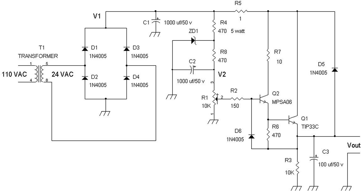
FIGURE 14.27 Fixing the DC power supply’s design, with improvements via emitter followers Q2 (MPSA06) and Q1 (TIP33C). Note: In keeping with the original schematic (Figure 14-26), R1 is designated as a potentiometer.
The transistors Q2 and Q1 are protected from over-current via current-limiting resistors R5 and R7, which are half-watt resistors. Should excessive current arise at Vout, these resistors can act like a fuse to save the transistors from burning out.
The “fixed” design now has capacitor C1 directly connected to the full-wave bridge rectifier circuit (D1 to D4) to provide a peak DC voltage of 24 volts × 1.414 ~ 34 volts DC. By using double emitter follower amplifiers, Q2 and Q1, and a well-filtered DC voltage at V2, this variable voltage power supply provides essentially ripple-free DC voltages at Vout. Q1’s emitter follower amplifier provides a low source resistance at Vout, which provides a “stiffer” voltage source than the collector output of the 2N307A transistor in Figure 14-26.
The DC voltage is regulated (e.g., if the power line (mains) voltage changes, so does Vout), as shown in Figure 14-27, via Zener diode ZD1 connected across C2. Typically, you want the Zener diode’s voltage to be lower than the raw 34 volts at V1. For example, you can try something like a 24-volt, 5-watt Zener diode (e.g., 1N5359B). Make sure R4 is at least a 2-watt resistor when you add the Zener diode. Of course, other Zener diode voltages can be used instead of 24 volts, such as 20 volts or 22 volts. Catch diodes D5 and D6 are added to prevent reverse bias breakdown of the transistors Q1 and Q2 when the power is turned off.
NOTE: Q1, TIP33C, should be on a heat sink insulated from ground.
An Example of the Missing Ground Connection
In our next circuit, a 3.00-MHz crystal oscillator, strange signals were measured on the oscilloscope. See Figures 14-28 (a), (b), and (c). The original circuit was built on a printed circuit board. All connections for the circuit appeared to be correct and resemble the circuit shown in Figure 14-28(c). However, output signal Vout in Figures 14-28 (a) and (b) showed incorrect DC voltages and waveforms. Vout should output a 3.00-MHz pulsed waveform close to 50 percent duty cycle from 0 volts to +5 volts. Let’s see what was found.
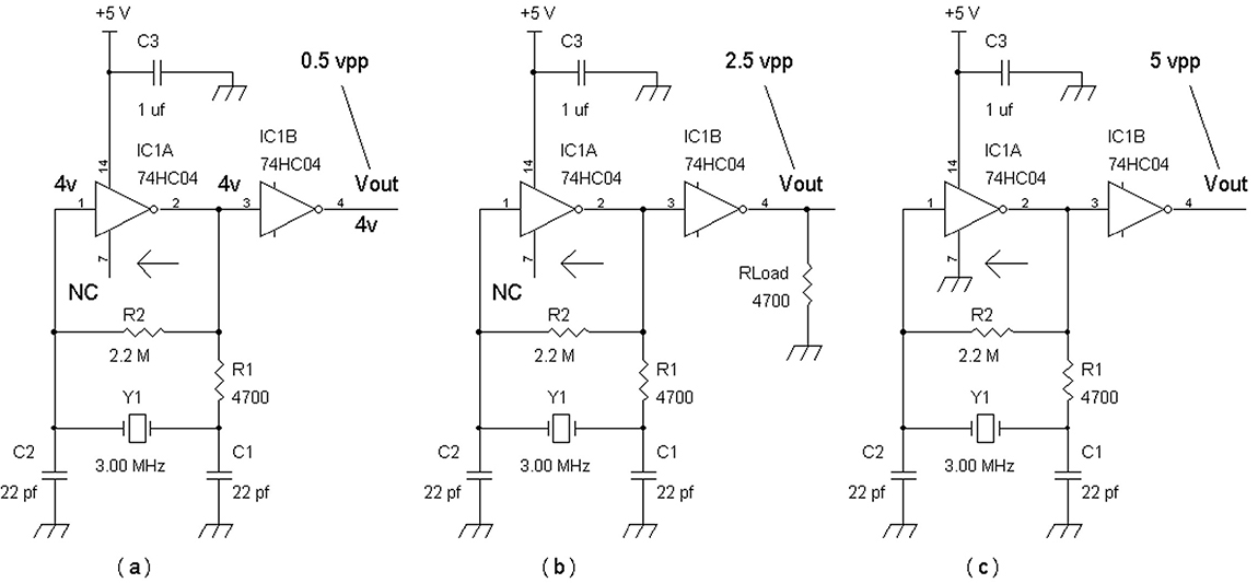
FIGURE 14.28 (a) No connection on ground pin 7; (b) no connection on pin 7 with test load resistor, RLoad; and (c) with ground connection re-established to provide proper output signal.
In Figure 14-28(a), it is not known yet that pin 7 of IC1A (74HC04) is not really connected to ground. By using a DVM or scope, the average DC voltage is checked at pins 1, 2, 3, and 4. If the 74HC04 logic inverters are working properly, we should measure about 2.5 volts average on all these pins because the oscillation waveform will be close to a 50 percent duty cycle pulse that goes from 0 volts to 5 volts. So, the average voltage would be 2.5 volts. Instead, as shown in Figure 14-28(a), we see that the average DC level is about 4 volts on pins 1, 2, 3, and 4. This would not make sense if the input to IC1B at pin 3 is 4 volts, a logic high voltage, then by “definition” the inverter gate’s output at pin 4 should be close to 0 volts. But this is not the case; output pin 4 is also about 4 volts. So, there is something wrong here. When we look closely for an oscillation signal, we see a small amplitude waveform shown in Figure 14-29. There are again problems with this waveform, as it is around 0.5 volts peak to peak and at the wrong frequency, 2.5 kHz, which is way off the crystal’s frequency of 3.00 MHz. Furthermore, the waveform does not resemble a 50 percent duty cycle pulse (square wave). Instead, it is a narrower duty cycle pulse.
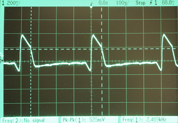
FIGURE 14.29 Vout of the circuit in Figure 14-28(a), an oscillating waveform at about 2.5 kHz, which is the incorrect frequency since the crystal is at 3.00 MHz.
The next thing to try is to see what happens if the output is loaded with 4700Ω as shown in Figure 14-28(b). We would expect no change in the waveform. But instead we see a larger amplitude waveform shown in Figure 14-30. The amplitude has increased from 0.5 volt peaked (with no load resistor) to 2.5 volts peak to peak. So, loading the output pin 4 unexpectedly increased signal level. This is indeed strange.
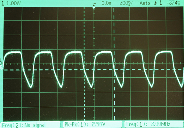
FIGURE 14.30 With Vout connected to an external 4700Ω load resistor, the frequency is now correct at 3.00 MHz, but the waveform shape and amplitude are incorrect.
Using an ohm meter, it was found that the 74HC04’s ground pin 7 was not tied to ground. After re-soldering the ground pin, the output signal looked normal as shown in Figure 14-31, and as depicted in the schematic in Figure 14-28(c).
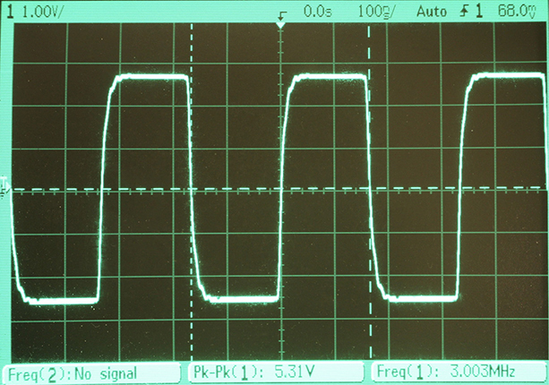
FIGURE 14.31 After connecting pin 7 of the 74HC04 chip to ground, Vout provided a 5-volt peak to peak signal at 3.00 MHz with the correct logic levels.
So, there are a couple of lessons here to take. One is to use an ohm meter to confirm the ground pin of the IC is really connected to ground. The other is that if you just scoped the waveforms and the logic levels are incorrect, check the ground pin for continuity to ground.
Ferrite Beads to Tame Parasitic Oscillations
When working with high-frequency oscillators, parasitic oscillations can occur. See Figure 14-32(a) and (b). Figure 14-32(b) provides a solution to stop parasitic oscillations via a base series resistor or using a series base ferrite bead.

FIGURE 14.32 (a) A Colpitts crystal oscillator that may not oscillate at the crystal frequency due to parasitic oscillations; (b) a Q1 base series 47Ω or ferrite bead to remove the parasitic oscillation.
The Colpitts oscillator uses a tuned circuit including inductor L2, variable capacitor VC_osc, and capacitive voltage divider circuit C4 and C5. Crystal Y1 works as a very high Q series resonant circuit. The variable capacitor is adjusted such that with L2 and C4 and C5, the circuit oscillates at the crystal frequency (e.g., 26.59 MHz). If there is not sufficient loop gain to sustain an oscillation, the loop gain can be increased. This can be achieved by having the collector current increased via lowering emitter bias resistor R3 (e.g., from 1000Ω to 560Ω), or the resistance of R4 may be increased twofold (e.g., to 68kΩ). Another way to increase loop gain is by decreasing C5’s capacitance (e.g., from 680 pf to 330 pf) to provide less attenuation via the capacitive C4/C5 voltage divider circuit. Also, C4’s capacitance may be increased from 33 pf to 39 pf while C5 can be decreased to 470 pf. Variable capacitor VC_osc will be readjusted to provide the (sustained) oscillation signal.
If the crystal oscillator’s frequency is changed to be ≥ 50 MHz, the inductor, L2, may need to be wound with thick gauge wire to ensure high Q at these very high frequencies. For example, L2 may be wound with 18 to 14 AWG (American Wire Gauge) wire.
Essentially, positive feedback is performed by coupling the signal at VC (collector) via the voltage divider C4 and C5 to the emitter terminal via crystal Y1 that acts as almost a short-circuit at the crystal’s stated frequency but a high impedance at other frequencies. The crystal then predominates in terms of setting the frequency and not L2, VC_osc, C4, and C5. Tuning VC_osc will vary the oscillator frequency extremely little, usually by less than 0.1 percent. By coupling the collector terminal’s signal into the emitter via C4, transistor Q1 is a grounded base amplifier that provides no signal inversion from emitter (as the input) to the collector (as an output terminal). Q1’s base is AC ground via the 0.01-μf capacitor C3. Note that if C3 is not low impedance at the oscillation frequency, the oscillator will not start up, and no signal will be at Vout. For example, if C3 is → 10 pf (due to soldering in a wrong value capacitor), the oscillator will not work (e.g., Vout → 0 volts AC) because at 26.59 MHz, a 10-pf capacitor has about 599Ω of impedance, which is too high an impedance value to effectively AC ground Q1’s base.
A capacitor with capacitance, C, has an impedance magnitude in ohms, |Zc| = 1/(2πfcrystal C), where C is measured in farads, and fcrystal is the crystal’s frequency in Hz. For example, if fcrystal is 26.59 MHz and C = 0.01 μf, then |Zc| = 1/(2πfcrystal C) = 1/(2π × 26.59 × 106 × 0.01 × 10–6) then we have in ohms: |Zc| = 1/(2π × 26.59 × 0.01) = 1/(1.67) = 0.599Ω. An easier estimation for finding the impedance magnitude of 0.01 μf = 10,000 pf is if we know from the previous paragraph that 10 pf at the same frequency, 26.59 MHz, has 599Ω for |Zc|, then we know that 0.01 μf equals 10,000 pf has to be 1000× lower in impedance magnitude of the 10-pf capacitor. The reason is the 10,000 pf is a 1000× multiple of 10 pf. Thus, the impedance drops from 599Ω to 599Ω/1000 = 0.599Ω. So, for all practical purposes, the 0.01-μf capacitor C3 is indeed like an AC short-circuit given its 0.599Ω impedance magnitude at the 26.59 MHz oscillation frequency.
The output signal is generally not taken from the collector terminal because any stray capacitances can detune the circuit easily. And if the collector terminal is loading into a medium to low resistance load (e.g., 1000Ω), then the oscillator can stop working due to (too much of a) reduced loop gain. Providing the output signal via the capacitive voltage divider at Vout generally gives the “cleanest” waveform. Capacitive voltage dividers C4 and C5 provide a lower impedance source, which can then drive other circuits. Emitter terminal signal VE can provide an output signal but it is a bit more distorted than the signal at Vout.
Figure 14-33 shows various implementations of adding series resistors and ferrite beads to a transistor to stop parasitic oscillations. This can be especially important if you use ultra-high-frequency (oscillator) transistors for Q1, such as the 2SA1161, a 3.5 GHz PNP transistor.
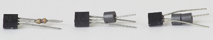
FIGURE 14.33 The left transistor has a solder series resistor, the center transistor has one ferrite bead slipped into its base lead, and the one on the right shows two ferrite beads installed.
One important item to note when using ferrite beads as shown in this photo, is to confirm with an ohm meter that the ferrite beads you slip into the transistor’s base lead are indeed non-conductive. There are ferrite beads that can be slightly conductive, which will partially short out the base, collector, and emitter. Use the 2MΩ setting on your ohm meter to confirm there is infinite resistance.
Generally, the series base resistor can be on a printed circuit board, but if there is no space or if the board inadvertently omitted the series base resistor, you can solder one in as shown on the left side of Figure 14-33. The actual resistance value depends on the frequency you are operating at. Normally, you can start with about 22Ω, but it can go as high as 220Ω. Alternatively, you can slip one or two ferrite beads into the base lead. Having two beads stacked in series is sometimes needed if the parasitic oscillation exists with one bead. If you have a longer ferrite bead, you can use that in place of two beads. Now let’s look at Figure 14-34, an output signal waveform from Figure 14-32(a) with some higher-frequency parasitic oscillation where the oscillator transistor (e.g., 2N3906) does not have a series resistor or ferrite bead.
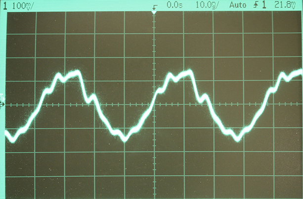
FIGURE 14.34 A “jagged” waveform at Vout due to a high-frequency parasitic oscillation signal riding on top of the lower frequency desired oscillator signal.
Now let’s see what happens when a single ferrite bead is inserted into the base lead of the same transistor (2N3906) to stop the parasitic oscillation. Figure 14-35 shows a much cleaner output waveform at Vout from Figure 14-28(b).
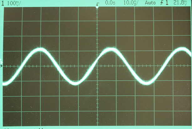
FIGURE 14.35 A single ferrite bead inserted into the oscillator transistor’s base lead results in a much cleaner Vout waveform.
Similar results were achieved using a 47Ω series base resistor in the oscillator transistor’s base lead. See Figure 14-36.
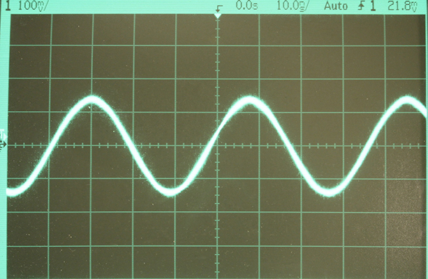
FIGURE 14.36 A series base resistor (e.g., 47Ω) stops the parasitic oscillation to deliver a cleaner sinusoidal waveform.
Summary
We showed in this chapter how to analyze not-so-well-designed circuits and then improved them. In some cases, the improvement or fix is just reversing the leads (e.g., the photodiode (D2PD) in Figure 14-10 or the capacitor (C7 = 100 µf) in Figure 14-23). Another example showed increasing the reliability of an audio power amplifier by adding a correct snubbing network at the output terminal (Figure 14-11, by adding series resistor Rext1 = 10Ω with C4 = 0.1 µf) to avoid inducing parasitic oscillations. Thus, troubleshooting sometimes requires that we look at the circuit design carefully because the original circuit may not have worked so well in the first place.