

Great code is aware of the underlying hardware on which it executes. Without question, the design of the central processing unit (CPU) has the greatest impact on the performance of your software. This chapter, and the next, discuss the design of CPUs and their instruction sets — information that is absolutely crucial for writing high-performance software.
A CPU is capable of executing a set of commands (or machine instructions), each of which accomplishes some small task. To execute a particular instruction, a CPU requires a certain amount of electronic circuitry specific to that instruction. Therefore, as you increase the number of instructions the CPU can support, you also increase the complexity of the CPU and you increase the amount of circuitry (logic gates) needed to support those instructions. To keep the number of logic gates on the CPU reasonably small (thus lowering the CPU’s cost), CPU designers must restrict the number and complexity of the instructions that the CPU is capable of executing. This small set of instructions is the CPU’s instruction set.
Programs in early computer systems were often “hardwired” into the circuitry. That is, the computer’s wiring determined exactly what algorithm the computer would execute. One had to rewire the computer in order to use the computer to solve a different problem. This was a difficult task, something that only electrical engineers were able to do. The next advance in computer design was the programmable computer system, one that allowed a computer operator to easily “rewire” the computer system using sockets and plug wires (a patch board system). A computer program consisted of rows of sockets, with each row representing one operation during the execution of the program. The programmer could determine which of several instructions would be executed by plugging a wire into the particular socket for the desired instruction (see Figure 9-1).
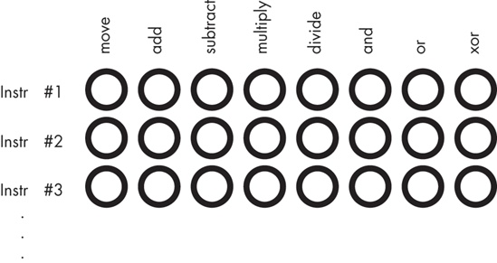
Of course, a major problem with this scheme was that the number of possible instructions was severely limited by the number of sockets one could physically place on each row. CPU designers quickly discovered that with a small amount of additional logic circuitry, they could reduce the number of sockets required for specifying n different instructions from n sockets to log2(n) sockets. They did this by assigning a unique numeric code to each instruction and then representing each code as a binary number (for example, Figure 9-2 shows how to represent eight instructions using only three bits).
The example in Figure 9-2 requires eight logic functions to decode the A, B, and C bits on the patch board, but the extra circuitry (a single three-line–to–eight-line decoder) is worth the cost because it reduces the total number of sockets from eight to three for each instruction.
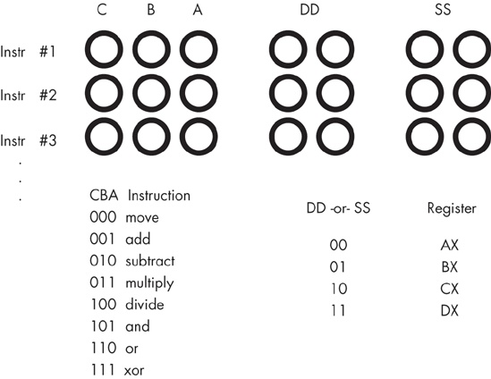
Of course, many CPU instructions do not stand alone. For example, a move instruction is a command that moves data from one location in the computer to another, such as from one register to another. The move instruction requires two operands: a source operand and a destination operand. The CPU’s designer usually encodes the source and destination operands as part of the machine instruction, with certain sockets corresponding to the source and certain sockets corresponding to the destination.
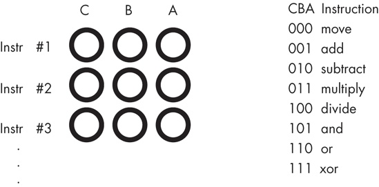
Figure 9-3 shows one possible combination of sockets that would handle this. The move instruction would move data from the source register to the destination register, the add instruction would add the value of the source register to the destination register, and so on. This scheme allows the encoding of 128 different instructions with just seven sockets per instruction.
One of the primary advances in computer design was the invention of the stored program computer. A big problem with patch-board programming was that the number of machine instructions in a program was limited by the number of rows of sockets available on the machine. Early computer designers recognized a relationship between the sockets on the patch board and bits in memory. They figured they could store the numeric equivalent of a machine instruction in main memory, fetch the instruction’s numeric equivalent from memory when the CPU wanted to execute the instruction, and then load that binary number into a special register to decode the instruction.
The trick was to add additional circuitry, called the control unit (CU), to the CPU. The control unit uses a special register, the instruction pointer, that holds the address of an instruction’s numeric code (also known as an operation code or opcode). The control unit fetches this instruction’s opcode from memory and places it in the instruction decoding register for execution. After executing the instruction, the control unit increments the instruction pointer and fetches the next instruction from memory for execution. This process repeats for each instruction the program executes.
The goal of the CPU’s designer is to assign an appropriate number of bits to the opcode’s instruction field and to its operand fields. Choosing more bits for the instruction field lets the opcode encode more instructions, just as choosing more bits for the operand fields lets the opcode specify a larger number of operands (often memory locations or registers). However, some instructions have only one operand, while others don’t have any operands at all. Rather than waste the bits associated with these operand fields for instructions that don’t have the maximum number of operands, the CPU designers often reuse these fields to encode additional opcodes, once again with some additional circuitry. The Intel 80x86 CPU family is a good example of this, with machine instructions ranging from 1 to almost 15 bytes long.[36]
Once the control unit fetches an instruction from memory, you may wonder, “Exactly how does the CPU execute this instruction?” In traditional CPU design there have been two common approaches used: hardwired logic and emulation (microcode). The 80x86 family, for example, uses both of these techniques.
A hardwired, or random logic,[37] approach uses decoders, latches, counters, and other hardware logic devices to operate on the opcode data. The micro-code approach involves a very fast but simple internal processor that uses the CPU’s opcodes as indexes into a table of operations called the microcode, and then executes a sequence of microinstructions that do the work of the macroinstruction they are emulating.
The random-logic approach has the advantage of decreasing the amount of time it takes to execute an opcode’s instruction, provided that typical CPU speeds are faster than memory speeds, a situation that has been true for quite some time. The drawback to the random-logic approach is that it is difficult to design the necessary circuitry for CPUs with large and complex instruction sets. The hardware logic that executes the instructions winds up requiring a large percentage of the chip’s real estate, and it becomes difficult to properly lay out the logic so that related circuits are close to one another in the two-dimensional space of the chip.
CPUs based on microcode contain a small, very fast execution unit (circuitry in the CPU that is responsible for executing a particular function) that uses the binary opcode to select a set of instructions from the microcode bank. This microcode executes one microinstruction per clock cycle, and the sequence of microinstructions executes all the steps to do whatever calculations are necessary for that instruction.
The microcode approach may appear to be substantially slower than the random-logic approach because of all the steps involved. But this isn’t necessarily true. Keep in mind that with a random-logic approach to instruction execution, a sequencer that steps through several states (one state per clock cycle) often makes up part of the random logic. Whether you use up clock cycles executing microinstructions or stepping through a random-logic state machine, you’re still burning up time.
However, microcode does suffer from one disadvantage compared to random logic: the speed at which the processor runs can be limited by the speed of the internal microcode execution unit. Although this micro-engine itself is usually quite fast, the micro-engine must fetch its instructions from the microcode ROM (read-only memory). Therefore, if memory technology is slower than the execution logic, the system will have to introduce wait states into the microcode ROM access, thus slowing the micro-engine down. However, micro-engines generally don’t support the use of wait states, so this means that the micro-engine must run at the same speed as the microcode ROM, which effectively limits the speed at which the micro-engine, and therefore the CPU, can run.
Which approach is better for CPU design? That depends entirely on the current state of memory technology. If memory technology is faster than CPU technology, the microcode approach tends to make more sense. If memory technology is slower than CPU technology, random logic tends to produce faster execution of machine instructions.
To be able to write great code, you need to understand how a CPU executes individual machine instructions. To that end, let’s consider four representative 80x86 instructions: mov, add, loop, and jnz (jump if not zero). By understanding these four instructions, you can get a good feel for how a CPU executes all the instructions in the instruction set.
The mov instruction copies the data from the source operand to the destination operand. The add instruction adds the value of its source operand to its destination operand. The loop and jnz instructions are conditional-jump instructions — they test some condition and then jump to some other instruction in memory if the condition is true, or continue with the next instruction if the condition is false. The jnz instruction tests a Boolean variable within the CPU known as the zero flag and either transfers control to the target instruction if the zero flag contains zero, or continues with the next instruction if the zero flag contains one. The program specifies the address of the target instruction (the instruction to jump to) by specifying the distance, in bytes, from the jnz instruction to the target instruction in memory.
The loop instruction decrements the value of the ECX register and transfers control to a target instruction if ECX does not contain zero (after the decrement). This is a good example of a Complex Instruction Set Computer (CISC) instruction because it does multiple operations:
It subtracts one from ECX.
It does a conditional jump if ECX does not contain zero.
That is, loop is roughly equivalent to the following instruction sequence:
sub( 1, ecx ); // On the 80x86, the sub instruction sets the zero flag
jnz SomeLabel; // the result of the subtraction is zero.
To execute the mov, add, jnz, and loop instructions, the CPU has to execute a number of different steps. Although each 80x86 CPU is different and doesn't necessarily execute the exact same steps, these CPUs do execute a similar sequence of operations. Each operation requires a finite amount of time to execute, and the time required to execute the entire instruction generally amounts to one clock cycle per operation or stage (as we usually refer to each of these steps) that the CPU executes. Obviously, the more steps needed for an instruction, the slower it will run. Complex instructions generally run slower than simple instructions, because complex instructions usually have many execution stages.
Although each CPU is different and may run different steps when executing instructions, the 80x86 mov(srcReg,destReg); instruction could use the following execution steps:
Fetch the instruction’s opcode from memory.
Update the EIP (extended instruction pointer) register with the address of the byte following the opcode.
Decode the instruction’s opcode to see what instruction it specifies.
Fetch the data from the source register (
srcReg).Store the fetched value into the destination register (
destReg).
The mov(srcReg,destMem); instruction could use the following execution steps:
Fetch the instruction’s opcode from memory.
Update the EIP register with the address of the byte following the opcode.
Decode the instruction’s opcode to see what instruction it specifies.
Fetch the displacement associated with the memory operand from the memory location immediately following the opcode.
Update EIP to point at the first byte beyond the operand that follows the opcode.
If the
movinstruction uses a complex addressing mode (for example, the indexed addressing mode), compute the effective address of the destination memory location.Fetch the data from
srcReg.Store the fetched value into the destination memory location.
Note that a mov(srcMem,destReg); instruction is very similar, simply swapping the register access for the memory access in these steps.
The mov(constant,destReg); instruction could use the following execution steps:
Fetch the instruction’s opcode from memory.
Update the EIP register with the address of the byte following the opcode.
Decode the instruction’s opcode to see what instruction it specifies.
Fetch the constant associated with the source operand from the memory location immediately following the opcode.
Update EIP to point at the first byte beyond the constant that follows the opcode.
Store the constant value into the destination register.
Assuming each step requires one clock cycle for execution, this sequence will require six clock cycles to execute.
The mov(constant,destMem); instruction could use the following execution steps:
Fetch the instruction’s opcode from memory.
Update the EIP register with the address of the byte following the opcode.
Decode the instruction’s opcode to see what instruction it specifies.
Fetch the displacement associated with the memory operand from the memory location immediately following the opcode.
Update EIP to point at the first byte beyond the operand that follows the opcode.
Fetch the constant operand’s value from the memory location immediately following the displacement associated with the memory operand.
Update EIP to point at the first byte beyond the constant.
If the
movinstruction uses a complex addressing mode (for example, the indexed addressing mode), compute the effective address of the destination memory location.Store the constant value into the destination memory location.
The add instruction is a little more complex. Here’s a typical set of operations that the add(srcReg,destReg); instruction must complete:
Fetch the instruction’s opcode from memory.
Update the EIP register with the address of the byte following the opcode.
Decode the instruction’s opcode to see what instruction it specifies.
Fetch the value of the source register and send it to the arithmetic logical unit (ALU), which handles arithmetic on the CPU.
Fetch the value of the destination register operand and send it to the ALU.
Instruct the ALU to add the values.
Store the result back into the destination register operand.
Update the flags register with the result of the addition operation.
Note
The flags register, also known as the condition-codes register or program-status word, is an array of Boolean variables in the CPU that tracks whether the previous instruction produced an overflow, a zero result, a negative result, or other such condition.
If the source operand is a memory location instead of a register, and the add instruction takes the form add(srcMem,destReg); then the operation is slightly more complicated:
Fetch the instruction’s opcode from memory.
Update the EIP register with the address of the byte following the opcode.
Decode the instruction’s opcode to see what instruction it specifies.
Fetch the displacement associated with the memory operand from the memory location immediately following the opcode.
Update EIP to point at the first byte beyond the operand that follows the opcode.
If the
addinstruction uses a complex addressing mode (for example, the indexed addressing mode), compute the effective address of the source memory location.Fetch the source operand’s data from memory and send it to the ALU.
Fetch the value of the destination register operand and send it to the ALU.
Instruct the ALU to add the values.
Store the result back into the destination register operand.
Update the flags register with the result of the addition operation.
If the source operand is a constant and the destination operand is a register, the add instruction takes the form add(constant,destReg); and here is how the CPU might deal with it:
Fetch the instruction’s opcode from memory.
Update the EIP register with the address of the byte following the opcode.
Decode the instruction’s opcode to see what instruction it specifies.
Fetch the constant operand that immediately follows the opcode in memory and send it to the ALU.
Update EIP to point at the first byte beyond the constant that follows the opcode.
Fetch the value of the destination register operand and send it to the ALU.
Instruct the ALU to add the values.
Store the result back into the destination register operand.
Update the flags register with the result of the addition operation.
This instruction sequence requires nine cycles to complete.
If the source operand is a constant, and the destination operand is a memory location, then the add instruction takes the form add(constant, dest-Mem); and the operation is slightly more complicated:
Update the EIP register with the address of the byte following the opcode.
Decode the instruction’s opcode to see what instruction it specifies.
Fetch the displacement associated with the memory operand from memory immediately following the opcode.
Update EIP to point at the first byte beyond the operand that follows the opcode.
If the
addinstruction uses a complex addressing mode (for example, the indexed addressing mode), compute the effective address of the destination memory location.Fetch the constant operand that immediately follows the memory operand’s displacement value and send it to the ALU.
Fetch the destination operand’s data from memory and send it to the ALU.
Update EIP to point at the first byte beyond the constant that follows the memory operand.
Instruct the ALU to add the values.
Store the result back into the destination memory operand.
Update the flags register with the result of the addition operation.
This instruction sequence requires 11 or 12 cycles to complete, depending on whether the effective address computation is necessary.
Because the 80x86 jnz instruction does not allow different types of operands, there is only one sequence of steps needed for this instruction. The jnz label; instruction might use the following sequence of steps:
Fetch the instruction’s opcode from memory.
Update the EIP register with the address of the displacement value following the instruction.
Decode the opcode to see what instruction it specifies.
Fetch the displacement value (the jump distance) and send it to the ALU.
Update the EIP register to hold the address of the instruction following the displacement operand.
Test the zero flag to see if it is clear (that is, if it contains zero).
If the zero flag was clear, copy the value in EIP to the ALU.
If the zero flag was clear, instruct the ALU to add the displacement and EIP values.
If the zero flag was clear, copy the result of the addition back to the EIP.
Notice how the jnz instruction requires fewer steps, and thus runs in fewer clock cycles, if the jump is not taken. This is very typical for conditional-jump instructions.
Because the 80x86 loop instruction does not allow different types of operands, there is only one sequence of steps needed for this instruction. The 80x86 loop instruction might use an execution sequence like the following:
Fetch the instruction’s opcode from memory.
Update the EIP register with the address of the displacement operand following the opcode.
Decode the opcode to see what instruction it specifies.
Fetch the value of the ECX register and send it to the ALU.
Instruct the ALU to decrement this value.
Send the result back to the ECX register. Set a special internal flag if this result is nonzero.
Fetch the displacement value (the jump distance) following the opcode in memory and send it to the ALU.
Update the EIP register with the address of the instruction following the displacement operand.
Test the special internal flag to see if ECX was nonzero.
If the flag was set (that is, it contains one), copy the value in EIP to the ALU.
If the flag was set, instruct the ALU to add the displacement and EIP values.
If the flag was set, copy the result of the addition back to the EIP register.
As with the jnz instruction, you’ll note that the loop instruction executes more rapidly if the branch is not taken and the CPU continues execution with the instruction that immediately follows the loop instruction.
If we can reduce the amount of time it takes for a CPU to execute the individual instructions appearing in that CPU’s instruction set, it should be fairly clear that an application containing a sequence of those instructions will also run faster (compared with executing that sequence on a CPU whose individual instructions have not been sped up). Though the steps associated with a particular instruction’s execution are usually beyond the control of a software engineer, understanding those steps and why the CPU designer chose an particular implementation for an instruction can help you pick more appropriate instruction sequences that execute faster.
An early goal of the Reduced Instruction Set Computer (RISC) processors was to execute one instruction per clock cycle, on the average. However, even if a RISC instruction is simplified, the actual execution of the instruction still requires multiple steps. So how could they achieve the goal? The answer is parallelism.
Consider the following steps for a mov(srcReg,destReg); instruction:
Fetch the instruction’s opcode from memory.
Update the EIP register with the address of the byte following the opcode.
Decode the instruction’s opcode to see what instruction it specifies.
Fetch the data from
srcReg.Store the fetched value into the destination register (
destReg).
There are five stages in the execution of this instruction, with certain dependencies existing between most of the stages. For example, the CPU must fetch the instruction’s opcode from memory before it updates the EIP register instruction with the address of the byte beyond the opcode. Likewise, the CPU won’t know that it needs to fetch the value of the source register until it decodes the instruction’s opcode. Finally, the CPU must fetch the value of the source register before it can store the fetched value in the destination register.
All but one of the stages in the execution of this mov instruction are serial. That is, the CPU must execute one stage before proceeding to the next. The one exception is step 2, updating the EIP register. Although this stage must follow the first stage, none of the following stages in the instruction depend upon this step. Therefore, this could be the third, forth, or fifth step in the calculation and it wouldn’t affect the outcome of the instruction. Further, we could execute this step concurrently with any of the other steps, and it wouldn’t affect the operation of the mov instruction. By doing two of the stages in parallel, we can reduce the execution time of this instruction by one clock cycle. The following list of steps illustrates one possible concurrent execution:
Fetch the instruction’s opcode from memory.
Decode the instruction’s opcode to see what instruction it specifies.
Fetch the data from
srcRegand update the EIP register with the address of the byte following the opcode.Store the fetched value into the destination register (
destReg).
Although the remaining stages in the mov(reg,reg); instruction must remain serialized, other forms of the mov instruction offer similar opportunities to save cycles by overlapping stages of their execution. For example, consider the 80x86 mov([ebx+disp],eax); instruction:
Fetch the instruction’s opcode from memory.
Update the EIP register with the address of the byte following the opcode.
Decode the instruction’s opcode to see what instruction it specifies.
Fetch the displacement value for use in calculating the effective address of the source operand.
Update EIP to point at the first byte after the displacement value in memory.
Compute the effective address of the source operand.
Fetch the value of the source operand’s data from memory.
Store the result into the destination register operand.
Once again, there is the opportunity to overlap the execution of several stages in this instruction. In the following example, we reduce the number of execution steps from eight to six by overlapping both updates of EIP with two other operations:
Fetch the instruction’s opcode from memory.
Decode the instruction’s opcode to see what instruction it specifies, and update the EIP register with the address of the byte following the opcode.
Fetch the displacement value for use in calculating the effective address of the source operand.
Compute the effective address of the source operand, and update EIP to point at the first byte after the displacement value in memory.
Fetch the value of the source operand’s data from memory.
Store the result into the destination register operand.
As a last example, consider the add(constant,[ebx+disp]); instruction (the instruction with the largest number of steps we’ve considered thus far). It’s non-overlapped execution looks like this:
Fetch the instruction’s opcode from memory.
Update the EIP register with the address of the byte following the opcode.
Decode the instruction’s opcode to see what instruction it specifies.
Fetch the displacement value from the memory location immediately following the opcode.
Update EIP to point at the first byte beyond the displacement operand that follows the opcode.
Compute the effective address of the second operand.
Fetch the constant operand that immediately follows the displacement value in memory and send it to the ALU.
Fetch the destination operand’s data from memory and send it to the ALU.
Update EIP to point at the first byte beyond the constant that follows the displacement operand.
Instruct the ALU to add the values.
Store the result back into the destination (second) operand.
Update the flags register with the result of the addition operation.
We can overlap several steps in this instruction by noting that certain stages don’t depend on the result of their immediate predecessor:
Decode the instruction’s opcode to see what instruction it specifies and update the EIP register with the address of the byte following the opcode.
Fetch the displacement value from the memory location immediately following the opcode.
Update EIP to point at the first byte beyond the displacement operand that follows the opcode and compute the effective address of the memory operand (EBX+disp).
Fetch the constant operand that immediately follows the displacement value and send it to the ALU.
Fetch the destination operand’s data from memory and send it to the ALU.
Instruct the ALU to add the values and update EIP to point at the first byte beyond the constant value
Store the result back into the second operand and update the flags register with the result of the addition operation.
Although it might seem possible to fetch the constant and the memory operand in the same step because their values do not depend upon one another, the CPU can’t actually do this (yet!) because it has only a single data bus, and both values are coming from memory. However, in the next section you’ll see how we can overcome this problem.
By overlapping various stages in the execution of these instructions, we’ve been able to substantially reduce the number of steps, and consequently the number of clock cycles, that the instructions need to complete execution. This process of executing various steps of the instruction in parallel with other steps is a major key to improving CPU performance without cranking up the clock speed on the chip. However, there’s only so much to be gained from this approach alone, because instruction execution is still serialized. Starting with the next section we’ll start to see how to overlap the execution of adjacent instructions in order to save additional cycles.
The key to improving the speed of a processor is to perform operations in parallel. If we were able to do two operations on each clock cycle, the CPU would execute instructions twice as fast when running at the same clock speed. However, simply deciding to execute two operations per clock cycle doesn’t make accomplishing it easy.
As you have seen, the steps of the add instruction that involve adding two values and then storing their sum cannot be done concurrently, because you cannot store the sum until after you’ve computed it. Furthermore, there are some resources that the CPU cannot share between steps in an instruction. There is only one data bus, and the CPU cannot fetch an instruction’s opcode while it is trying to store some data to memory. In addition, many of the steps that make up the execution of an instruction share functional units in the CPU. Functional units are groups of logic that perform a common operation, such as the arithmetic logical unit (ALU) and the control unit (CU). A functional unit is only capable of one operation at a time. You cannot do two operations concurrently that use the same functional unit. To design a CPU that executes several steps in parallel, one must arrange those steps to reduce potential conflicts, or add additional logic so the two (or more) operations can occur simultaneously by executing in different functional units.
Consider again the steps a mov(srcMem, destReg ); instruction might require:
Fetch the instruction’s opcode from memory.
Update the EIP register to hold the address of the displacement value following the opcode.
Decode the instruction’s opcode to see what instruction it specifies.
Fetch the displacement value from memory to compute the source operand’s effective address.
Update the EIP register to hold the address of the byte beyond the displacement value.
Compute the effective address of the source operand.
Fetch the value of the source operand.
Store the fetched value into the destination register.
The first operation uses the value of the EIP register, so we cannot overlap it with the subsequent step, which adjusts the value in EIP. In addition, the first operation uses the bus to fetch the instruction opcode from memory, and because every step that follows this one depends upon this opcode, it is unlikely we will be able to overlap this first step with any other.
The second and third operations do not share any functional units, and the third operation doesn’t depend upon the value of the EIP register, which is modified in the second step. Therefore, we can easily modify the control unit so that it combines these steps, adjusting the EIP register at the same time that it decodes the instruction. This will shave one cycle off the execution of the mov instruction.
The third and fourth steps, which decode the instruction’s opcode and fetch the displacement value, do not look like they can be done in parallel because you must decode the instruction’s opcode to determine whether the CPU needs to fetch a displacement operand from memory. However, we can design the CPU to go ahead and fetch the displacement anyway, so that it’s available if we need it.
Of course, there is no way to overlap the execution of steps 7 and 8 in the mov instruction because it must surely fetch the value before storing it away.
By combining all the steps that are possible, we might obtain the following for a mov instruction:
Fetch the instruction’s opcode from memory.
Decode the instruction’s opcode to see what instruction it specifies, and update the EIP register to hold the address of the displacement value following the opcode.
Fetch the displacement value from memory to compute the source operand’s effective address, and update the EIP register to hold the address of the byte beyond the displacement value.
Compute the effective address of the source operand.
Fetch the value of the source operand from memory.
By adding a small amount of logic to the CPU, we’ve shaved one or two cycles off the execution of the mov instruction. This simple optimization works with most of the other instructions as well.
Now that we’ve looked at some simple optimization techniques, consider what happens when the mov instruction executes on a CPU with a 32-bit data bus. If the mov instruction fetches an 8-bit displacement value from memory, the CPU may actually wind up fetching an additional three bytes along with the displacement value (the 32-bit data bus lets us fetch four bytes in a single bus cycle). The second byte on the data bus is actually the opcode of the next instruction. If we could save this opcode until the execution of the next instruction, we could shave a cycle off its execution time because it would not have to fetch the same opcode byte again.
Can we make any more improvements? The answer is yes. Note that during the execution of the mov instruction, the CPU is not accessing memory on every clock cycle. For example, while storing the data into the destination register, the bus is idle. When the bus is idle, we can prefetch and save the instruction opcode and operands of the next instruction.
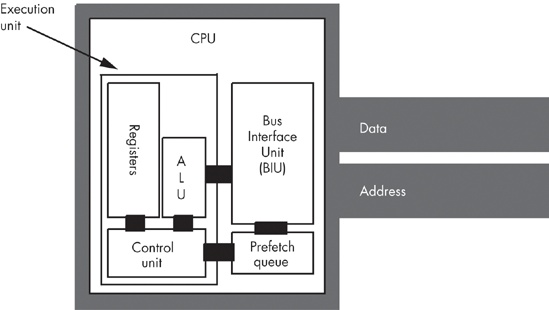
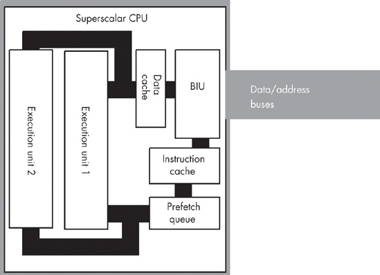
The hardware that does this is the prefetch queue. Figure 9-4 shows the internal organization of a CPU with a prefetch queue. The Bus Interface Unit (BIU), as its name implies, is responsible for controlling access to the address and data buses. The BIU acts as a “traffic cop” and handles simultaneous requests for bus access by different modules, such as the execution unit and the prefetch queue. Whenever some component inside the CPU wishes to access main memory, it sends this request to the BIU.
Whenever the execution unit is not using the BIU, the BIU can fetch additional bytes from the memory that holds the machine instructions and store them in the prefetch queue. Then, whenever the CPU needs an instruction opcode or operand value, it grabs the next available byte from the prefetch queue. Because the BIU grabs multiple bytes at a time from memory, and because, per clock cycle, it generally consumes fewer bytes from the prefetch queue than are in the queue, instructions will normally be sitting in the prefetch queue for the CPU’s use.
Note, however, that we’re not guaranteed that all instructions and operands will be sitting in the prefetch queue when we need them. For example, consider the 80x86 jnz Label; instruction. If the 2-byte form of the instruction appears at locations 400 and 401 in memory, the prefetch queue may contain the bytes at addresses 402, 403, 404, 405, 406, 407, and so on. Now consider what happens if jnz transfers control to Label. If the target address of the jnz instruction is 480, the bytes at addresses 402, 403, 404, and so on, won’t be of any use to the CPU. The system will have to pause for a moment to fetch the data at address 480 before it can go on. Most of the time the CPU fetches sequential values from memory, though, so having the data in the prefetch queue saves time.
Another improvement we can make is to overlap decoding of the next instruction’s opcode with the execution of the last step of the previous instruction. After the CPU processes the operand, the next available byte in the prefetch queue is an opcode, and the CPU can decode it in anticipation of its execution, because the instruction decoder is idle while the CPU executes the steps of the current instruction. Of course, if the current instruction modifies the EIP register, any time spent decoding the next instruction goes to waste, but as this decoding of the next instruction occurs in parallel with other operations of the current instruction, it does not slow down the system (though it does require extra circuitry to do this).
Our instruction execution sequence now assumes that the following CPU prefetch events are occurring in the background (and concurrently):
If the prefetch queue is not full (generally it can hold between 8 and 32 bytes, depending on the processor) and the BIU is idle on the current clock cycle, fetch the next double word located at the address found in the EIP register at the beginning of the clock cycle.
If the instruction decoder is idle and the current instruction does not require an instruction operand, the CPU should begin decoding the opcode at the front of the prefetch queue. If the current instruction requires an instruction operand, then the CPU begins decoding the byte just beyond that operand in the prefetch queue.
Now let’s reconsider our mov(srcreg,destreg); instruction from 9.4 Parallelism — The Key to Faster Processing. Because we’ve added the prefetch queue and the BIU, fetching and decoding opcode bytes and updating the EIP register takes place in parallel with the execution of specific stages of the previous instruction. Without the BIU and the prefetch queue, the mov(reg,reg); instruction would require the following steps:
Fetch the instruction’s opcode from memory.
Decode the instruction’s opcode to see what instruction it specifies.
Fetch the source register and update the EIP register with the address of the next instruction.
Store the fetched value into the destination register.
However, now that we can overlap the fetch and decode stages of this instruction with specific stages of the previous instruction, we get the following steps:
Fetch and decode the instruction — this is overlapped with the previous instruction.
Fetch the source register and update the EIP register with the address of the next instruction.
Store the fetched value into the destination register.
The instruction execution timings in this last example make a couple of optimistic assumptions — namely that the opcode is already present in the prefetch queue and that the CPU has already decoded it. If either is not true, additional cycles will be necessary to fetch the opcode from memory and decode the instruction.
Because they invalidate the prefetch queue, jump and conditional-jump instructions are slower than other instructions when the jump instructions actually transfer control to the target location. The CPU cannot overlap fetching and decoding of the opcode for the next instruction with the execution of a jump instruction that transfers control. Therefore, it may take several cycles after the execution of one of these jump instructions for the prefetch queue to recover. If you want to write fast code, avoid jumping around in your program as much as possible.
Note that the conditional-jump instructions only invalidate the prefetch queue if they actually transfer control to the target location. If the jump condition is false, then execution continues with the next instruction and the values in the prefetch queue remain valid. Therefore, if you can determine, while writing the program, which jump condition occurs most frequently, you should arrange your program so that the most common condition causes the program to continue with the next instruction rather than jump to a separate location.
In addition, instruction size in bytes can affect the performance of the prefetch queue. The larger the instruction, the faster the CPU will empty the prefetch queue. Instructions involving constants and memory operands tend to be the largest. If you execute a sequence of these instructions in a row, the CPU may wind up having to wait because it is removing instructions from the prefetch queue faster than the BIU is copying data to the prefetch queue. Therefore, you should attempt to use shorter instructions whenever possible because they will improve the performance of the prefetch queue.
Finally, prefetch queues work best when you have a wide data bus. The 16-bit 8086 processor runs much faster than the 8-bit 8088 because it can keep the prefetch queue full with fewer bus accesses. Don’t forget, the CPU needs to use the bus for other purposes. Instructions that access memory compete with the prefetch queue for access to the bus. If you have a sequence of instructions that all access memory, the prefetch queue may quickly become empty if there are only a few bus cycles available for filling the prefetch queue during the execution of these instructions. Of course, once the prefetch queue is empty, the CPU must wait for the BIU to fetch new opcodes from memory before it can continue executing instructions.
Executing instructions in parallel using a BIU and an execution unit is a special case of pipelining. Most modern processors incorporate pipelining to improve performance. With just a few exceptions, we’ll see that pipelining allows us to execute one instruction per clock cycle.
The advantage of the prefetch queue is that it lets the CPU overlap fetching and decoding the instruction opcode with the execution of other instructions. That is, while one instruction is executing, the BIU is fetching and decoding the next instruction. Assuming you’re willing to add hardware, you can execute almost all operations in parallel. That is the idea behind pipelining.
Pipelined operation improves the average performance of an application by executing several instructions concurrently. However, as you saw with the prefetch queue, certain instructions and certain combinations of instructions fare better than others in a pipelined system. By understanding how pipelined operation works, you can organize your applications to run faster.
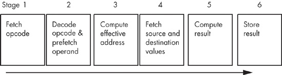
Consider the steps necessary to do a generic operation:
Fetch the instruction's opcode from memory.
Decode the opcode and, if required, prefetch a displacement operand, a constant operand, or both.
If required, compute the effective address for a memory operand (e.g., [ebx+disp]).
If required, fetch the value of any memory operand and/or register.
Compute the result.
Store the result into the destination register.
Each of the steps in this sequence uses a separate tick of the system clock (Time = 1, Time = 2, Time = 3, and so on, represent consecutive ticks of the clock).
Assuming you’re willing to pay for some extra silicon, you can build a little miniprocessor to handle each of these steps. The organization would look something like Figure 9-5.
Note the stages we’ve combined. For example, in stage 4 of Figure 9-5 the CPU fetches both the source and destination operands in the same step. You can do this by putting multiple data paths inside the CPU (such as from the registers to the ALU) and ensuring that no two operands ever compete for simultaneous use of the data bus (that is, there are no memory-to-memory operations).
If you design a separate piece of hardware for each stage in the pipeline in Figure 9-5, almost all these steps can take place in parallel. Of course, you cannot fetch and decode the opcode for more than one instruction at the same time, but you can fetch the opcode of the next instruction while decoding the current instruction’s opcode. If you have an n-stage pipeline, you will usually have n instructions executing concurrently. Figure 9-6 shows pipelining in operation. T1, T2, T3, and so on, represent consecutive “ticks” (Time = 1, Time = 2, and so on) of the system clock.
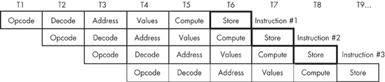
At time T = T1, the CPU fetches the opcode byte for the first instruction. At T = T2, the CPU begins decoding the opcode for the first instruction, and, in parallel, it fetches a block of bytes from the prefetch queue in the event that the first instruction has an operand. Also in parallel with the decoding of the first instruction, the CPU instructs the BIU to fetch the opcode of the second instruction because the first instruction no longer needs that circuitry. Note that there is a minor conflict here. The CPU is attempting to fetch the next byte from the prefetch queue for use as an operand; at the same time it is fetching operand data from the prefetch queue for use as an opcode. How can it do both at once? You’ll see the solution shortly.
At time T = T3, the CPU computes the address of any memory operand if the first instruction accesses memory. If the first instruction does not use an addressing mode requiring such computation, the CPU does nothing. During T3, the CPU also decodes the opcode of the second instruction and fetches any operands the second instruction has. Finally, the CPU also fetches the opcode for the third instruction. With each advancing tick of the clock, another step in the execution of each instruction in the pipeline completes, and the CPU fetches the opcode of yet another instruction from memory.
This process continues until at T = T6 the CPU completes the execution of the first instruction, computes the result for the second, and fetches the opcode for the sixth instruction in the pipeline. The important thing to see is that after T = T5, the CPU completes an instruction on every clock cycle. Once the CPU fills the pipeline, it completes one instruction on each cycle. This is true even if there are complex addressing modes to be computed, memory operands to fetch, or other operations that consume cycles on a nonpipelined processor. All you need to do is add more stages to the pipe-line, and you can still effectively process each instruction in one clock cycle.
Now back to the small conflict in the pipeline organization I mentioned earlier. At T = T2, for example, the CPU attempts to prefetch a block of bytes containing any operands of the first instruction, and at the same time it fetches the opcode of the second instruction. Until the CPU decodes the first instruction, it doesn’t know how many operands the instruction requires nor does it know their length. Moreover, the CPU doesn't know what byte to fetch as the opcode of the second instruction until it determines the length of any operands the first instruction requires. So how can the pipeline fetch the opcode of the next instruction in parallel with any address operands of the current instruction?
One solution is to disallow this simultaneous operation in order to avoid the potential data hazard (more about data hazards later). If an instruction has an address or constant operand, we can simply delay the start of the next instruction. Unfortunately, many instructions have these additional operands, so this approach will have a substantial negative impact on the execution speed of the CPU.
The second solution is to throw a lot more hardware at the problem. Operand and constant sizes usually come in 1-, 2-, and 4-byte lengths. Therefore, if we actually fetch the bytes in memory that are located at offsets one, three, and five bytes beyond the current opcode we are decoding, one of these three bytes will probably contain the opcode of the next instruction. Once we are through decoding the current instruction, we know how many bytes it consumes, and, therefore, we know the offset of the next opcode. We can use a simple data selector circuit to choose which of the three candidate opcode bytes we want to use.
In practice, we actually have to select the next opcode byte from more than three candidates because 80x86 instructions come in many different lengths. For example, a mov instruction that copies a 32-bit constant to a memory location can be 10 or more bytes long. Moreover, instructions vary in length from 1 to 15 bytes. And some opcodes on the 80x86 are longer than 1 byte, so the CPU may have to fetch multiple bytes in order to properly decode the current instruction. However, by throwing more hardware at the problem we can decode the current opcode at the same time we’re fetching the next.
Unfortunately, the scenario presented in the previous section is a little too simplistic. There are two problems that our simple pipeline ignores: competition between instructions for access to the bus (known as bus contention), and nonsequential instruction execution. Both problems may increase the average execution time of the instructions in the pipeline. By understanding how the pipeline works, you can write your software to avoid problems in the pipeline and improve the performance of your applications.
Bus contention can occur whenever an instruction needs to access an item in memory. For example, if a mov(reg,mem); instruction needs to store data in memory and a mov(mem,reg); instruction is reading data from memory, contention for the address and data bus may develop because the CPU will be trying to fetch data from memory and write data to memory simultaneously.
One simplistic way to handle bus contention is through a pipeline stall. The CPU, when faced with contention for the bus, gives priority to the instruction farthest along in the pipeline. This causes the later instruction in the pipeline to stall, and it takes two cycles to execute that instruction (see Figure 9-7).
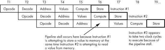
There are many other cases of bus contention. For example, fetching operands for an instruction requires access to the prefetch queue at the same time that the CPU needs to access the queue to fetch the opcode of the next instruction. Given the simple pipelining scheme that we’ve outlined so far, it’s unlikely that most instructions would execute at one clock (cycle) per instruction (CPI).
As another example of a pipeline stall, consider what happens when an instruction modifies the value in the EIP register? For example, the jnz instruction might change the value in the EIP register if it conditionally transfers control to its target label. This, of course, implies that the next set of instructions to be executed does not immediately follow the instruction that modifies EIP. By the time the instruction jnz label; completes execution (assuming the zero flag is clear, so that the branch is taken), we’ve already started five other instructions and we’re only one clock cycle away from the completion of the first of these. Obviously, the CPU must not execute those instructions, or it will compute improper results.
The only reasonable solution is to flush the entire pipeline and begin fetching opcodes anew. However, doing so causes a severe execution-time penalty. It will take the length of the pipeline (six cycles in our example) before the next instruction completes execution. The longer the pipeline is, the more you can accomplish per cycle in the system, but the slower a program will run if it jumps around quite a bit. Unfortunately, you cannot control the number of stages in the pipeline,[38] but you can control the number of transfer instructions that appear in your programs. Obviously, you should keep these to a minimum in a pipelined system.
System designers can resolve many problems with bus contention through the intelligent use of the prefetch queue and the cache memory subsystem. As you have seen, they can design the prefetch queue to buffer data from the instruction stream. However, they can also use a separate instruction cache (apart from the data cache) to hold machine instructions. Though, as a programmer, you have no control over the cache organization of your CPU, knowing how the instruction cache operates on your particular CPU may allow you to use certain instruction sequences that would otherwise create stalls.
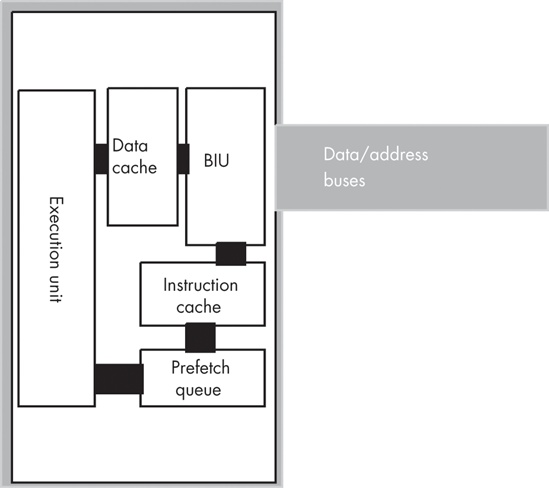
Suppose, for a moment, that the CPU has two separate memory spaces, one for instructions and one for data, each with its own bus. This is called the Harvard architecture because the first such machine was built at Harvard. On a Harvard machine there would be no contention for the bus. The BIU could continue to fetch opcodes on the instruction bus while accessing memory on the data/memory bus (see Figure 9-8).

In the real world, there are very few true Harvard machines. The extra pins needed on the processor to support two physically separate buses increase the cost of the processor and introduce many other engineering problems. However, microprocessor designers have discovered that they can obtain many benefits of the Harvard architecture with few of the disadvantages by using separate on-chip caches for data and instructions. Advanced CPUs use an internal Harvard architecture and an external von Neumann architecture. Figure 9-9 shows the structure of the 80x86 with separate data and instruction caches.
Each path between the sections inside the CPU represents an independent bus, and data can flow on all paths concurrently. This means that the prefetch queue can be pulling instruction opcodes from the instruction cache while the execution unit is writing data to the data cache. However, it is not always possible, even with a cache, to avoid bus contention. In the arrangement with two separate caches, the BIU still has to use the data/address bus to fetch opcodes from memory whenever they are not located in the instruction cache. Likewise, the data cache still has to buffer data from memory occasionally.
Although you cannot control the presence, size, or type of cache on a CPU, you must be aware of how the cache operates in order to write the best programs. On-chip level-one instruction caches are generally quite small (between 4 KB and 64 KB on typical CPUs) compared to the size of main memory. Therefore, the shorter your instructions, the more of them will fit in the cache (getting tired of “shorter instructions” yet?). The more instructions you have in the cache, the less often bus contention will occur. Likewise, using registers to hold temporary results places less strain on the data cache, so it doesn’t need to flush data to memory or retrieve data from memory quite so often.
There is another problem with using a pipeline: hazards. There are two types of hazards: control hazards and data hazards. We’ve actually discussed control hazards already, although we did not refer to them by that name. A control hazard occurs whenever the CPU branches to some new location in memory and consequently has to flush from the pipeline the instructions that are in various stages of execution. The system resources used to begin the execution of the instructions the CPU flushes from the pipeline could have been put to more productive use, had the programmer organized the application to minimize the number of these instructions. So by understanding the effects of hazards on your code, you can write faster applications.
Let’s take a look at data hazards using the execution profile for the following instruction sequence:
mov( SomeVar, ebx );
mov( [ebx], eax );
When these two instructions execute, the pipeline will look something like what is shown in Figure 9-10.
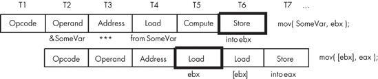
These two instructions attempt to fetch the 32-bit value whose address is held in the SomeVar pointer variable. However, this sequence of instructions won’t work properly! Unfortunately, the second instruction has already accessed the value in EBX before the first instruction copies the address of memory location SomeVar into EBX (T5 and T6 in Figure 9-10).
CISC processors, like the 80x86, handle hazards automatically. (Some RISC chips do not, and if you tried this sequence on certain RISC chips you would store an incorrect value in EAX.) In order to handle the data hazard in this example, CISC processors stall the pipeline to synchronize the two instructions. The actual execution would look something like what is shown in Figure 9-11.
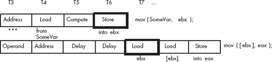
By delaying the second instruction by two clock cycles, the CPU guarantees that the load instruction will load EAX with the value at the proper address. Unfortunately, the mov([ebx],eax); instruction now executes in three clock cycles rather than one. However, requiring two extra clock cycles is better than producing incorrect results.
Fortunately, you (or your compiler) can reduce the impact that hazards have on program execution speed within your software. Note that a data hazard occurs when the source operand of one instruction was a destination operand of a previous instruction. There is nothing wrong with loading EBX from SomeVar and then loading EAX from [EBX]] (that is, the double-word memory location pointed at by EBX), as long as they don’t occur one right after the other. Suppose the code sequence had been:
mov( 2000, ecx );
mov( SomeVar, ebx );
mov( [ebx], eax );
We could reduce the effect of the hazard in this code sequence by simply rearranging the instructions. Let’s do that to obtain the following:
mov( SomeVar, ebx );
mov( 2000, ecx );
mov( [ebx], eax );
Now the mov([ebx],eax); instruction requires only one additional clock cycle rather than two. By inserting yet another instruction between the mov(SomeVar,ebx); and the mov([ebx],eax); instructions, you can eliminate the effects of the hazard altogether (of course, the inserted instruction must not modify the values in the EAX and EBX registers).
On a pipelined processor, the order of instructions in a program may dramatically affect the performance of that program. If you are writing assembly code, always look for possible hazards in your instruction sequences. Eliminate them wherever possible by rearranging the instructions. If you are using a compiler, choose a good compiler that properly handles instruction ordering.
With the pipelined architecture shown so far, we could achieve, at best, execution times of one CPI (clock per instruction). Is it possible to execute instructions faster than this? At first glance you might think, “Of course not, we can do at most one operation per clock cycle. So there is no way we can execute more than one instruction per clock cycle.” Keep in mind, however, that a single instruction is not a single operation. In the examples presented earlier, each instruction has taken between six and eight operations to complete. By adding seven or eight separate units to the CPU, we could effectively execute these eight operations in one clock cycle, yielding one CPI. If we add more hardware and execute, say, 16 operations at once, can we achieve 0.5 CPI? The answer is a qualified yes. A CPU that includes this additional hardware is a superscalar CPU, and it can execute more than one instruction during a single clock cycle. The 80x86 family began supporting superscalar execution with the introduction of the Pentium processor.
A superscalar CPU has several execution units (see Figure 9-12). If it encounters in the prefetch queue two or more instructions that can execute independently, it will do so.
There are a couple of advantages to going superscalar. Suppose you have the following instructions in the instruction stream:
mov( 1000, eax );
mov( 2000, ebx );
If there are no other problems or hazards in the surrounding code, and all six bytes for these two instructions are currently in the prefetch queue, there is no reason why the CPU cannot fetch and execute both instructions in parallel. All it takes is extra silicon on the CPU chip to implement two execution units.
Besides speeding up independent instructions, a superscalar CPU can also speed up program sequences that have hazards. One limitation of normal CPUs is that once a hazard occurs, the offending instruction will completely stall the pipeline. Every instruction that follows the stalled instruction will also have to wait for the CPU to synchronize the execution of the offending instructions. With a superscalar CPU, however, instructions following the hazard may continue execution through the pipeline as long as they don’t have hazards of their own. This alleviates (though it does not eliminate) some of the need for careful instruction scheduling.
The way you write software for a superscalar CPU can dramatically affect its performance. First and foremost is that rule you’re probably sick of by now: use short instructions. The shorter your instructions are, the more instructions the CPU can fetch in a single operation and, therefore, the more likely the CPU will execute faster than one CPI. Most superscalar CPUs do not completely duplicate the execution unit. There might be multiple ALUs, floating-point units, and so on, which means that certain instruction sequences can execute very quickly, while others won’t. You have to study the exact composition of your CPU to decide which instruction sequences produce the best performance.
In a standard superscalar CPU, it is the programmer’s (or compiler’s) responsibility to schedule (arrange) the instructions to avoid hazards and pipeline stalls. Fancier CPUs can actually remove some of this burden and improve performance by automatically rescheduling instructions while the program executes. To understand how this is possible, consider the following instruction sequence:
mov( SomeVar, ebx );
mov( [ebx], eax );
mov( 2000, ecx );
A data hazard exists between the first and second instructions. The second instruction must delay until the first instruction completes execution. This introduces a pipeline stall and increases the running time of the program. Typically, the stall affects every instruction that follows. However, note that the third instruction’s execution does not depend on the result from either of the first two instructions. Therefore, there is no reason to stall the execution of the mov(2000,ecx); instruction. It may continue executing while the second instruction waits for the first to complete. This technique is called out-of-order execution because the CPU can execute instructions prior to the completion of instructions appearing previously in the code stream.
Clearly, the CPU may only execute instructions out of sequence if doing so produces exactly the same results as in-order execution. While there are many little technical issues that make this problem more difficult than it seems, it is possible to implement this feature with enough engineering effort.
One problem that hampers the effectiveness of superscalar operation on the 80x86 CPU is the 80x86’s limited number of general-purpose registers. Suppose, for example, that the CPU had four different pipelines and, therefore, was capable of executing four instructions simultaneously. Presuming no conflicts existed among these instructions and they could all execute simultaneously, it would still be very difficult to actually achieve four instructions per clock cycle because most instructions operate on two register operands. For four instructions to execute concurrently, you’d need eight different registers: four destination registers and four source registers (none of the destination registers could double as source registers of other instructions). CPUs that have lots of registers can handle this task quite easily, but the limited register set of the 80x86 makes this difficult. Fortunately, there is a way to alleviate part of the problem through register renaming.
Register renaming is a sneaky way to give a CPU more registers than it actually has. Programmers will not have direct access to these extra registers, but the CPU can use them to prevent hazards in certain cases. For example, consider the following short instruction sequence:
mov( 0, eax );
mov( eax, i );
mov( 50, eax );
mov( eax, j );
Clearly, a data hazard exists between the first and second instructions and, likewise, a data hazard exists between the third and fourth instructions. Out-of-order execution in a superscalar CPU would normally allow the first and third instructions to execute concurrently, and then the second and fourth instructions could execute concurrently. However, a data hazard of sorts also exists between the first and third instructions because they use the same register. The programmer could have easily solved this problem by using a different register (say, EBX) for the third and fourth instructions. However, let’s assume that the programmer was unable to do this because all the other registers were all holding important values. Is this sequence doomed to executing in four cycles on a superscalar CPU that should only require two?
One advanced trick a CPU can employ is to create a bank of registers for each of the general-purpose registers on the CPU. That is, rather than having a single EAX register, the CPU could support an array of EAX registers; let’s call these registers EAX[0], EAX[1], EAX[2], and so on. Similarly, you could have an array of each of the other registers, so we could also have EBX[0]..EBX[n], ECX[0]..ECX[n], and so on. The instruction set does not give the programmer the ability to select one of these specific register array elements for a given instruction, but the CPU can automatically choose among the register array elements if doing so would not change the overall computation and could speed up the execution of the program. For example, consider the following sequence (with register array elements automatically chosen by the CPU):
mov( 0, eax[0] );
mov( eax[0], i );
mov( 50, eax[1] );
mov( eax[1], j );
Because EAX[0] and EAX[1] are different registers, the CPU can execute the first and third instructions concurrently. Likewise, the CPU can execute the second and fourth instructions concurrently.
This code provides an example of register renaming. Although this is a simple example, and different CPUs implement register renaming in many different ways, this example does demonstrate how the CPU can improve performance in certain instances using this technique.
Superscalar operation attempts to schedule, in hardware, the execution of multiple instructions simultaneously. Another technique, which Intel is using in its IA-64 architecture, involves very long instruction words, or VLIW. In a VLIW computer system, the CPU fetches a large block of bytes (41 bits in the case of the IA-64 Itanium CPU) and decodes and executes this block all at once. This block of bytes usually contains two or more instructions (three in the case of the IA-64). VLIW computing requires the programmer or compiler to properly schedule the instructions in each block so that there are no hazards or other conflicts, but if properly scheduled, the CPU can execute three or more instructions per clock cycle.
The Intel IA-64 architecture is not the only computer system to employ a VLIW architecture. Transmeta’s Crusoe processor family also uses a VLIW architecture. The Crusoe processor is different from the IA-64 architecture, insofar as it does not support native execution of IA-32 instructions. Instead, the Crusoe processor dynamically translates 80x86 instructions to Crusoe’s VLIW instructions. This “code morphing” technology results in code running about 50 percent slower than native code, though the Crusoe processor has other advantages.
We will not consider VLIW computing any further here because the technology is just becoming available (and it’s difficult to predict how it will impact system designs). Nevertheless, Intel and some other semiconductor manufacturers feel that it’s the wave of the future, so keep your eye on it.
Most techniques for improving CPU performance via architectural advances involve the parallel execution of instructions. The techniques up to this point in this chapter can be treated as if they were transparent to the programmer. That is, the programmer does not have to do anything special to take minimal advantage of pipeline and superscalar operation. As you have seen, if programmers are aware of the underlying architecture, they can write code that runs faster, but these architectural advances often improve performance significantly even if programmers do not write special code to take advantage of them.
The only problem with ignoring the underlying architecture is that there is only so much the hardware can do to parallelize a program that requires sequential execution for proper operation. To truly produce a parallel program, the programmer must specifically write parallel code, though, of course, this does require architectural support from the CPU. This section and the next touch on the types of support a CPU can provide.
Common CPUs use what is known as the Single Instruction, Single Data (SISD) model. This means that the CPU executes one instruction at a time, and that instruction operates on a single piece of data.[39] Two common parallel models are the so-called Single Instruction, Multiple Data (SIMD) and Multiple Instruction, Multiple Data (MIMD) models. As it turns out, many modern CPUs, including the 80x86, also include limited support for these latter two parallel-execution models, providing a hybrid SISD/SIMD/MIMD architecture.
In the SIMD model, the CPU executes a single instruction stream, just like the pure SISD model. However, in the SIMD model, the CPU operates on multiple pieces of data concurrently rather than on a single data object. For example, consider the 80x86 add instruction. This is a SISD instruction that operates on (that is, produces) a single piece of data. True, the instruction fetches values from two source operands, but the end result is that the add instruction will store a sum into only a single destination operand. An SIMD version of add, on the other hand, would compute the sum of several values simultaneously. The Pentium III’s MMX and SIMD instruction extensions, and the PowerPC’s AltaVec instructions, operate in exactly this fashion. With the paddb MMX instruction, for example, you can add up to eight separate pairs of values with the execution of a single instruction. Here’s an example of this instruction:
paddb( mm0, mm1 );
Although this instruction appears to have only two operands (like a typical SISD add instruction on the 80x86), the MMX registers (MM0 and MM1) actually hold eight independent byte values (the MMX registers are 64 bits wide but are treated as eight 8-bit values rather than as a single 64-bit value).
Note that SIMD instructions are only useful in specialized situations. Unless you have an algorithm that can take advantage of SIMD instructions, they’re not that useful. Fortunately, high-speed 3-D graphics and multimedia applications benefit greatly from these SIMD (and MMX) instructions, so their inclusion in the 80x86 CPU offers a huge performance boost for these important applications.
The MIMD model uses multiple instructions, operating on multiple pieces of data (usually with one instruction per data object, though one of these instructions could also operate on multiple data items). These multiple instructions execute independently of one another, so it’s very rare that a single program (or, more specifically, a single thread of execution) would use the MIMD model. However, if you have a multiprogramming environment with multiple programs attempting to execute concurrently, the MIMD model does allow each of those programs to execute their own code stream simultaneously. This type of parallel system is called a multiprocessor system.
Pipelining, superscalar operation, out-of-order execution, and VLIW designs are techniques that CPU designers use in order to execute several operations in parallel. These techniques support fine-grained parallelism and are useful for speeding up adjacent instructions in a computer system. If adding more functional units increases parallelism, you might wonder what would happen if you added another CPU to the system. This technique, known as multi-processing, can improve system performance, though not as uniformly as other techniques.
Multiprocessing doesn’t help a program’s performance unless that program is specifically written for use on a multiprocessor system. If you build a system with two CPUs, those CPUs cannot trade off executing alternate instructions within a single program. In fact, it is very expensive, time-wise, to switch the execution of a program’s instructions from one processor to another. Therefore, multiprocessor systems are only effective with an operating system that executes multiple processes or threads concurrently. To differentiate this type of parallelism from that afforded by pipelining and superscalar operation, we’ll call this kind of parallelism coarse-grained parallelism.
Adding multiple processors to a system is not as simple as wiring two or more processors to the motherboard. To understand why this is so, consider two separate programs running on separate processors in a multiprocessor system. Suppose also that these two processors communicate with one another by writing to a block of shared physical memory. Unfortunately, when CPU 1 attempts to writes to this block of memory it caches the data (locally on the CPU) and might not actually write the data to physical memory for some time. If CPU 2 attempts to simultaneously read this block of shared memory, it winds up reading the old data out of main memory (or its local cache) rather than reading the updated data that CPU 1 wrote to its local cache. This is known as the cache-coherency problem. In order for these two functions to operate properly, the two CPUs must notify each other whenever they make changes to shared objects, so the other CPU can update its local, cached copy.
One area where the RISC CPUs have a big advantage over Intel’s CPUs is in the support for multiple processors in a system. While Intel 80x86 systems reach a point of diminishing returns at around 16 processors, Sun SPARC and other RISC processors easily support 64-CPU systems (with more arriving, it seems, every day). This is why large databases and large Web server systems tend to use expensive Unix-based RISC systems rather than 80x86 systems.
Newer versions of the Pentium IV and Xeon processors support a hybrid form of multiprocessing known as hyperthreading. The idea behind hyper-threading is deceptively simple — in a typical superscalar processor it is rare for an instruction sequence to utilize all the CPU’s functional units on each clock cycle. Rather than allow those functional units to go unused, the CPU can run two separate threads of execution concurrently and keep all the CPU’s functional units occupied. This allows a single CPU to, effectively, do the work of 1.5 CPUs in a typical multiprocessor system.
The in-depth study of computer architecture could very well be considered a “follow-on course” to the material this chapter presents. There are many college and professional texts on computer architecture available today. Patterson and Hennessy’s Computer Architecture: A Quantitative Approach is one of the better regarded texts on this subject (though it is a bit heavily biased towards RISC architectures).
One subject missing from this chapter is the design of the CPU’s actual instruction set. That is the subject of the next chapter in this book.
[36] Though this is, by no means, the most complex instruction set. The VAX, for example, has instructions up to 150 bytes long!
[37] There is actually nothing random about this logic at all. This design technique gets its name from the fact that if you view a photomicrograph of a CPU die that uses microcode, the microcode section looks very regular; the same photograph of a CPU that utilizes random logic contains no such easily discernible patterns.
[38] Note, by the way, that the number of stages in an instruction pipeline varies among CPUs.
[39] We will ignore the parallelism provided by pipelining and superscalar operation in this discussion.