

This chapter describes the basic components that make up a computer system: the CPU, memory, I/O, and the bus that connects them. Although you can write software without this knowledge, writing great, high-performance code requires an understanding of this material.
This chapter begins by discussing bus organization and memory organization. These two hardware components may have as large a performance impact on your software as the CPU’s speed. Knowing about memory performance characteristics, data locality, and cache operation can help you design software that runs as fast as possible. Writing great code requires a strong knowledge of the computer’s architecture.
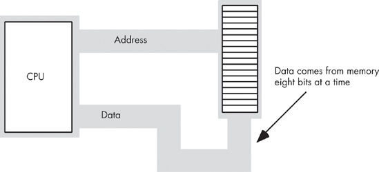
The basic operational design of a computer system is called its architecture. John von Neumann, a pioneer in computer design, is given credit for the principal architecture in use today. For example, the 80x86 family uses the von Neumann architecture (VNA). A typical von Neumann system has three major components: the central processing unit (CPU), memory, and input/output (I/O), as shown in Figure 6-1.
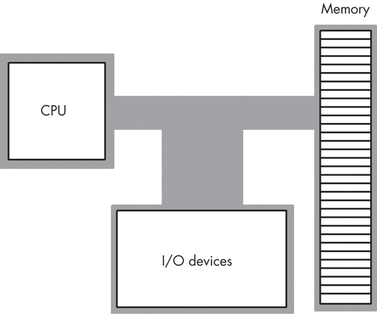
In VNA machines, like the 80x86, the CPU is where all the action takes place. All computations occur within the CPU. Data and machine instructions reside in memory until the CPU requires them, at which point the system transfers the data into the CPU. To the CPU, most I/O devices look like memory; the major difference between memory and I/O devices is the fact that the latter are generally located in the outside world, whereas the former is located within the same machine.
The system bus connects the various components of a VNA machine. Most CPUs have three major buses: the address bus, the data bus, and the control bus. A bus is a collection of wires on which electrical signals pass between components of the system. These buses vary from processor to processor, but each bus carries comparable information on most processors. For example, the data buses on the Pentium and 80386 may have different implementations, but both variants carry data between the processor, I/O, and memory.
CPUs use the data bus to shuffle data between the various components in a computer system. The size of this bus varies widely among CPUs. Indeed, bus size is one of the main attributes that defines the “size” of the processor.
Most modern, general-purpose CPUs employ a 32-bit-wide or 64-bit-wide data bus. Some processors use 8-bit or 16-bit data buses, there may well be some CPUs with 128-bit buses by the time you read this. For the most part, however, the CPUs in personal computers tend to use 32-bit or 64-bit data buses (and 64-bit data buses are the most prevalent).
You’ll often hear a processor called an 8-, 16-, 32-, or 64-bit processor. The smaller of the number of data lines on the processor and the size of the largest general-purpose integer register determines the processor size. For example, modern Intel 80x86 CPUs all have 64-bit buses, but only provide 32-bit general-purpose integer registers, so we’ll classify these devices as 32-bit processors. The AMD x86-64 processors support 64-bit integer registers and a 64-bit bus, so they’re 64-bit processors.
Although the 80x86 family members with 8-, 16-, 32-, and 64-bit data buses can process data blocks up to the bit width of the bus, they can also access smaller memory units of 8, 16, or 32 bits. Therefore, anything you can do with a small data bus can be done with a larger data bus as well; the larger data bus, however, may access memory faster and can access larger chunks of data in one memory operation. You’ll read about the exact nature of these memory accesses a little later in this chapter.
The data bus on an 80x86 family processor transfers information between a particular memory location or I/O device and the CPU. The only question is, “Which memory location or I/O device?” The address bus answers that question. To uniquely identify each memory location and I/O device, the system designer assigns a unique memory address to each. When the software wants to access a particular memory location or I/O device, it places the corresponding address on the address bus. Circuitry within the device checks this address and transfers data if there is an address match. All other memory locations ignore the request on the address bus.
With a single address bus line, a processor could access exactly two unique addresses: zero and one. With n address lines, the processor can access 2n unique addresses (because there are 2n unique values in an n-bit binary number). Therefore, the number of bits on the address bus will determine the maximum number of addressable memory and I/O locations. Early 80x86 processors, for example, provided only 20 lines on the address bus. Therefore, they could only access up to 1,048,576 (or 220) memory locations. Larger address buses can access more memory (see Table 6-1 on the next page).
Newer processors will support 40-, 48-, and 64-bit address buses. The time is coming when most programmers will consider 4 GB (gigabytes) of storage to be too small, just as we consider 1 MB (megabyte) insufficient today. (There was a time when 1 MB was considered far more than anyone would ever need!) Many other processors (such as SPARC and IA-64) already provide much larger addresses buses and, in fact, support addresses up to 64 bits in the software.
A 64-bit address range is truly infinite as far as memory is concerned. No one will ever put 264 bytes of memory into a computer system and feel that they need more. Of course, people have made claims like this in the past. A few years ago, no one ever thought a computer would need 1 GB of memory, but computers with a gigabyte of memory or more are very common today. However, 264 really is infinity for one simple reason — it’s physically impossible to build that much memory based on estimates of the current size of the universe (which estimate about 256 different elementary particles in the universe). Unless you can attach one byte of memory to every elementary particle in the known universe, you’re not even going to come close to approaching 264 bytes of memory on a given computer system. Then again, maybe we really will use whole planets as computer systems one day, as Douglas Adams predicts in The Hitchhiker’s Guide to the Galaxy. Who knows?
The control bus is an eclectic collection of signals that control how the processor communicates with the rest of the system. To illustrate its importance, consider the data bus for a moment. The CPU uses the data bus to move data between itself and memory. This prompts the question, “How does the system know whether it is sending or receiving data?” Well, the system uses two lines on the control bus, read and write, to determine the data flow direction (CPU to memory, or memory to CPU). So when the CPU wants to write data to memory, it asserts (places a signal on) the write control line. When the CPU wants to read data from memory, it asserts the read control line.
Although the exact composition of the control bus varies among processors, some control lines are common to all processors and are worth a brief mention. Among these are the system clock lines, interrupt lines, byte enable lines, and status lines.
The byte enable lines appear on the control bus of some CPUs that support byte-addressable memory. These control lines allow 16-, 32-, and 64-bit processors to deal with smaller chunks of data by communicating the size of the accompanying data. Additional details appear later in the sections on 16-bit and 32-bit buses.
The control bus also contains a signal that helps distinguish between address spaces on the 80x86 family of processors. The 80x86 family, unlike many other processors, provides two distinct address spaces: one for memory and one for I/O. However, it does not have two separate physical address buses (for I/O and memory). Instead, the system shares the address bus for both I/O and memory addresses. Additional control lines decide whether the address is intended for memory or I/O. When such signals are active, the I/O devices use the address on the LO 16 bits of the address bus. When inactive, the I/O devices ignore the signals on the address bus, and the memory subsystem takes over at that point.
A typical CPU addresses a maximum of 2n different memory locations, where n is the number of bits on the address bus (most computer systems built around 80x86 family CPUs do not include the maximum addressable amount of memory). Of course, the first question you should ask is, “What exactly is a memory location?” The 80x86, as an example, supports byte-addressable memory. Therefore, the basic memory unit is a byte. With address buses containing 20, 24, 32, or 36 address lines, the 80x86 processors can address 1 MB, 16 MB, 4 GB, or 64 GB of memory, respectively. Some CPU families do not provide byte-addressable memory (commonly, they only address memory in double-word or even quad-word chunks). However, because of the vast amount of software written that assumes memory is byte-addressable (such as all those C/C++ programs out there), even CPUs that don’t support byte-addressable memory in hardware still use byte addresses and simulate byte addressing in software. We’ll return to this issue shortly.
Think of memory as an array of bytes. The address of the first byte is zero and the address of the last byte is 2n−1. For a CPU with a 20-bit address bus, the following pseudo-Pascal array declaration is a good approximation of memory:
Memory: array [0..1048575] of byte; // One-megabyte address space (20 bits)
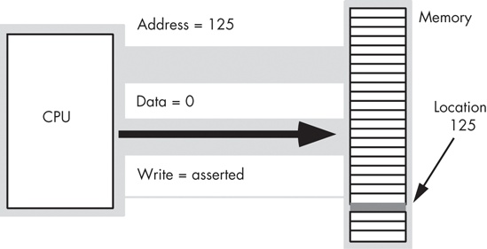
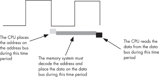
To execute the equivalent of the Pascal statement Memory [125] := 0; the CPU places the value zero on the data bus, the address 125 on the address bus, and asserts the write line on the control bus, as in Figure 6-2 on the next page.
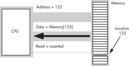
To execute the equivalent of CPU := Memory [125]; the CPU places the address 125 on the address bus, asserts the read line on the control bus, and then reads the resulting data from the data bus (see Figure 6-3).
This discussion applies only when accessing a single byte in memory. What happens when the processor accesses a word or a double word? Because memory consists of an array of bytes, how can we possibly deal with values larger than eight bits?
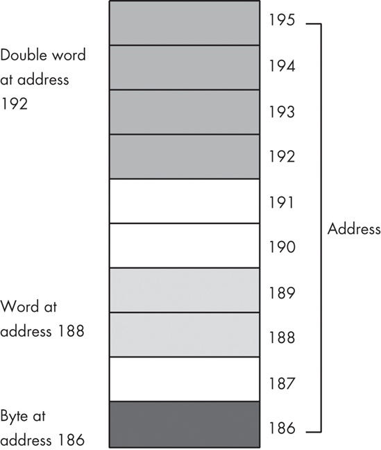
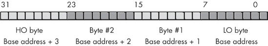
Different computer systems have different solutions to this problem. The 80x86 family stores the LO byte of a word at the address specified and the HO byte at the next location. Therefore, a word consumes two consecutive memory addresses (as you would expect, because a word consists of two bytes). Similarly, a double word consumes four consecutive memory locations.
The address for a word or a double word is the address of its LO byte. The remaining bytes follow this LO byte, with the HO byte appearing at the address of the word plus one or the address of the double word plus three (see Figure 6-4). Note that it is quite possible for byte, word, and double-word values to overlap in memory. For example, in Figure 6-4, you could have a word variable beginning at address 193, a byte variable at address 194, and a double-word value beginning at address 192. Bytes, words, and double words may begin at any valid address in memory. We will soon see, however, that starting larger objects at an arbitrary address is not a good idea.
A processor with an 8-bit bus (like the old 8088 CPU) can transfer 8 bits of data at a time. Because each memory address corresponds to an 8-bit byte, an 8-bit bus turns out to be the most convenient architecture (from the hardware perspective), as Figure 6-5 shows.
The term byte-addressable memory array means that the CPU can address memory in chunks as small as a single byte. It also means that this is the smallest unit of memory you can access at once with the processor. That is, if the processor wants to access a 4-bit value, it must read eight bits and then ignore the extra four bits.
It is also important to realize that byte addressability does not imply that the CPU can access eight bits starting at any arbitrary bit boundary. When you specify address 125 in memory, you get the entire eight bits at that address — nothing less, nothing more. Addresses are integers; you cannot specify, for example, address 125.5 to fetch fewer than eight bits or to fetch a byte straddling 2-byte addresses.
Although CPUs with an 8-bit data bus conveniently manipulate byte values, they can also manipulate word and double-word values. However, this requires multiple memory operations because these processors can only move eight bits of data at once. To load a word requires two memory operations; to load a double word requires four memory operations.
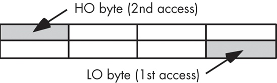
Some CPUs (such as the 8086, the 80286, and variants of the ARM/StrongARM processor family) have a 16-bit data bus. This allows these processors to access twice as much memory in the same amount of time as their 8-bit counterparts. These processors organize memory into two banks: an “even” bank and an “odd” bank (see Figure 6-6).
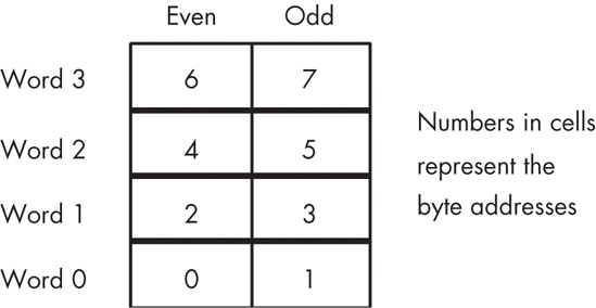
Figure 6-7 illustrates the data bus connection to the CPU. In this figure, the data bus lines D0 through D7 transfer the LO byte of the word, while bus lines D8 through D15 transfer the HO byte of the word.
The 16-bit members of the 80x86 family can load a word from any arbitrary address. As mentioned earlier, the processor fetches the LO byte of the value from the address specified and the HO byte from the next consecutive address. However, this creates a subtle problem if you look closely at Figure 6-7. What happens when you access a word that begins on an odd address? Suppose you want to read a word from location 125. The LO byte of the word comes from location 125 and the HO byte of the word comes from location 126. It turns out that there are two problems with this approach.
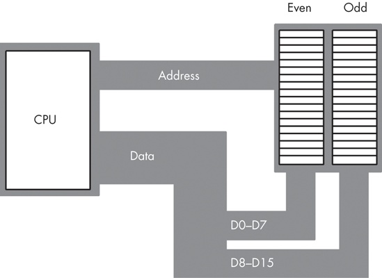
As you can see in Figure 6-7, data bus lines 8 through 15 (the HO byte) connect to the odd bank, and data bus lines 0 through 7 (the LO byte) connect to the even bank. Accessing memory location 125 will transfer data to the CPU on lines D8 through D15 of the data bus, placing the data in the HO byte; yet we need this in the LO byte! Fortunately, the 80x86 CPUs automatically recognize and handle this situation.
The second problem is even more obscure. When accessing words, we’re really accessing two separate bytes, each of which has a separate byte address. So the question arises, “What address appears on the address bus?” The 16-bit 80x86 CPUs always place even addresses on the bus. Bytes at even addresses always appear on data lines D0 through D7, and the bytes at odd addresses always appear on data lines D8 through D15. If you access a word at an even address, the CPU can bring in the entire 16-bit chunk in one memory operation. Likewise, if you access a single byte, the CPU activates the appropriate bank (using a byte-enable control line) and transfers that byte on the appropriate data lines for its address.
So, what happens when the CPU accesses a word at an odd address, like the example given earlier? The CPU cannot place the address 125 on the address bus and read the 16 bits from memory. There are no odd addresses coming out of a 16-bit 80x86 CPU — the addresses are always even. Therefore, if you try to put 125 on the address bus, 124 will actually appear on the bus. Were you to read the 16 bits at this address, you would get the word at addresses 124 (LO byte) and 125 (HO byte) — not what you’d expect. Accessing a word at an odd address requires two memory operations. First, the CPU must read the byte at address 125, and then it needs to read the byte at address 126. Finally, it needs to swap the positions of these bytes internally because both entered the CPU on the wrong half of the data bus.
Fortunately, the 16-bit 80x86 CPUs hide these details from you. Your programs can access words at any address and the CPU will properly access and swap (if necessary) the data in memory. However, accessing a word at an odd address will require two memory operations (just as with the 8-bit bus on the 8088/80188), so accessing words at odd addresses on a 16-bit processor is slower than accessing words at even addresses. By carefully arranging how you use memory, you can improve the speed of your programs on these CPUs.
Accessing 32-bit quantities always takes at least two memory operations on the 16-bit processors. If you access a 32-bit quantity at an odd address, a 16-bit processor may require three memory operations to access the data.
The 80x86 processors with a 32-bit data bus (such as the 80386 and 80486) use four banks of memory connected to the 32-bit data bus (see Figure 6-8).
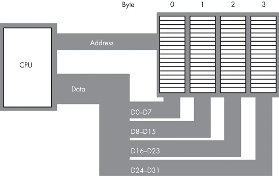
With a 32-bit memory interface, the 80x86 CPU can access any single byte with one memory operation. With a 16-bit memory interface the address placed on the address bus is always an even number, and similarly with a 32-bit memory interface, the address placed on the address bus is always some multiple of four. Using various byte-enable control lines, the CPU can select which of the four bytes at that address the software wants to access. As with the 16-bit processor, the CPU will automatically rearrange bytes as necessary.
A 32-bit CPU can also access a word at most memory addresses using a single memory operation, though word accesses at certain addresses will take two memory operations (see Figure 6-9). This is the same problem encountered with the 16-bit processor attempting to retrieve a word with an odd LO byte address, except it occurs half as often — only when the LO byte address divided by four leaves a remainder of three.
A 32-bit CPU can access a double word in a single memory operation only if the address of that value is evenly divisible by four. If not, the CPU may require two memory operations.
Once again, the 80x86 CPU handles all this automatically. However, there is a performance benefit to proper data alignment. Generally, the LO byte of word values should always be placed at even addresses, and the LO byte of double-word values should always be placed at addresses that are evenly divisible by four.
The Pentium and later processors provide a 64-bit data bus and special cache memory that reduces the impact of nonaligned data access. Although there may still be a penalty for accessing data at an inappropriate address, modern x86 CPUs suffer from the problem less frequently than the earlier CPUs. The discussion in 6.4.3 Cache Memory, will look at the details.
Although the 80x86 processor is not the only processor around that will let you access a byte, word, or double-word object at an arbitrary byte address, most processors created in the past 30 years do not allow this. For example, the 68000 processor found in the original Apple Macintosh system will allow you to access a byte at any address, but will raise an exception if you attempt to access a word at an odd address.[29] Many processors require that you access an object at an address that is an even multiple of the object’s size or the CPU will raise an exception.
Most RISC processors, including those found in modern Power Macintosh systems, do not allow you to access byte and word objects at all. Most RISC CPUs require that all data accesses be the same size as the data bus (or general-purpose integer register size, whichever is smaller). This is generally a double-word (32-bit) access. If you want to access a byte or a word on such a machine, you have to treat bytes and words as packed fields and use the shift and mask techniques to extract or insert byte and word data in a double word. Although it is nearly impossible to avoid byte accesses in software that does any character and string processing, if you expect your software to run on various modern RISC CPUs, you should avoid word data types in favor of double words if you don’t want to pay a performance penalty for the word accesses.
Earlier, you read that the 80x86 CPU family stores the LO byte of a word or double-word value at a particular address in memory and the successive HO bytes at successively higher addresses. There was also a vague statement to the effect that “different processors handle this in different ways.” Well, now is the time to learn how different processors store multi-byte objects in byte-addressable memory.
Almost every CPU you’ll use whose “bit size” is some power of two (8, 16, 32, 64, and so on) will number the bits and nibbles as shown in the previous chapters. There are some exceptions, but they are rare, and most of the time they represent a notational change, not a functional change (meaning you can safely ignore the difference). Once you start dealing with objects larger than eight bits, however, life becomes more complicated. Different CPUs organize the bytes in a multibyte object differently.
Consider the layout of the bytes in a double word on an 80x86 CPU (see Figure 6-10 ). The LO byte, which contributes the smallest component of a binary number, sits in bit positions zero through seven and appears at the lowest address in memory. It seems reasonable that the bits that contribute the least would be located at the lowest address in memory.
Unfortunately, this is not the only organization that is possible. Some CPUs, for example, reverse the memory addresses of all the bytes in a double word, using the organization shown in Figure 6-11.
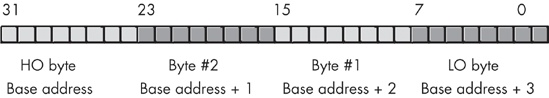
The Apple Macintosh and most non-80x86 Unix boxes use the data organization appearing in Figure 6-11. Therefore, this isn’t some rare and esoteric convention; it’s quite common. Furthermore, even on 80x86 systems, certain protocols (such as network transmissions) specify the data organization for double words as shown in Figure 6-11. So this isn’t something you can ignore if you work on PCs.
The byte organization that Intel uses is whimsically known as the little endian byte organization. The alternate form is known as big endian byte organization. If you’re wondering, these terms come from Jonathan Swift’s Gulliver’s Travels; the Lilliputians were arguing over whether one should open an egg by cracking it on the little end or the big end, a parody of the arguments the Catholics and Protestants were having over their respective doctrines when Swift was writing.
The time for arguing over which format is better was back before there were several different CPUs created using different byte genders. (Many programmers refer to this as byte sex. Byte gender is a little less offensive, hence the use of that term in this book.) Today, we have to deal with the fact that different CPUs sport different byte genders, and we have to take care when writing software if we want that software to run on both types of processors. Arguing over whether one format is better than another is irrelevant at this point; regardless of which format is better or worse, we may have to put extra code in our programs to deal with both formats (including the worse of the two, whichever that is).
The big endian versus little endian problem occurs when we try to pass binary data between two computers. For example, the double-word binary representation of 256 on a little endian machine has the following byte values:
LO byte:     0
Byte #1:     1
Byte #2:     0
HO byte:     0
If you assemble these four bytes on a little endian machine, their layout takes this form:
Byte:        3    2    1    0
256:         0    0    1    0    (each digit represents an 8-bit value)
On a big endian machine, however, the layout takes the following form:
Byte:        3    2    1    0
256:         0    1    0    0    (each digit represents an 8-bit value)
This means that if you take a 32-bit value from one of these machines and attempt to use it on the other machine (whose byte gender is not the same), you won’t get correct results. For example, if you take a big endian version of the value 256, you’ll discover that it has the bit value one in bit position 16 in the little endian format. If you try to use this value on a little endian machine, that machine will think that the value is actually 65,536 (that is, %1_0000_0000_0000_0000). Therefore, when exchanging data between two different machines, the best solution is to convert your values to some canonical form and then, if necessary, convert the canonical form back to the local format if the local and canonical formats are not the same. Exactly what constitutes a “canonical” format depends, usually, on the transmission medium. For example, when transmitting data across networks, the canonical form is usually big endian because TCP/IP and some other network protocols use the big endian format. This does not suggest that big endian is always the canonical form. For example, when transmitting data across the Universal Serial Bus (USB), the canonical format is little endian. Of course, if you control the software on both ends, the choice of canonical form is arbitrary; still, you should attempt to use the appropriate form for the transmission medium to avoid confusion down the road.
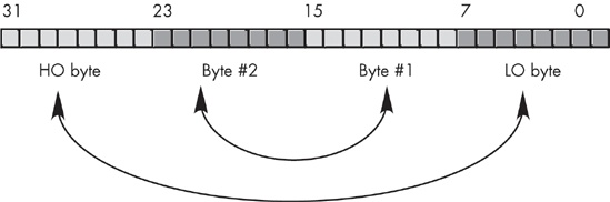
To convert between the endian forms, you must do a mirror-image swap of the bytes in the object. To cause a mirror-image swap, you must swap the bytes at opposite ends of the binary number, and then work your way towards the middle of the object swapping pairs of bytes as you go along. For example, to convert between the big endian and little endian format within a double word, you’d first swap bytes zero and three, then you’d swap bytes one and two (see Figure 6-12).
For word values, all you need to do is swap the HO and LO bytes to change the byte gender. For quad-word values, you need to swap bytes zero and seven, one and six, two and five, and three and four. Because very little software deals with 128-bit integers, you’ll probably not need to worry about long-word gender conversion, but the concept is the same if you do.
Note that the byte gender conversion process is reflexive. That is, the same algorithm that converts big endian to little endian also converts little endian to big endian. If you run the algorithm twice, you wind up with the data in the original format.
Even if you’re not writing software that exchanges data between two computers, the issue of byte gender may arise. To illustrate this point, consider that some programs assemble larger objects from discrete bytes by assigning those bytes to specific positions within the larger value. If the software puts the LO byte into bit positions zero through seven (little endian format) on a big endian machine, the program will not produce correct results. Therefore, if the software needs to run on different CPUs that have different byte organizations, the software will have to determine the byte gender of the machine it’s running on and adjust how it assembles larger objects from bytes accordingly.
To illustrate how to build larger objects from discrete bytes, perhaps the best place to start is with a short example that first demonstrates how one could assemble a 32-bit object from four individual bytes. The most common way to do this is to create a discriminant union structure that contains a 32-bit object and a 4-byte array:
Note
Many languages, but not all, support the discriminant union data type. For example, in Pascal, you would instead use a case variant record. See your language reference manual for details.
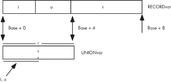
For those who are not familiar with unions, they are a data structure similar to records or structs except the compiler allocates the storage for each field of the union at the same address in memory. Consider the following two declarations from the C programming language:
struct
{
        short unsigned i;   // Assume shorts require 16 bits.
        short unsigned u;
        long unsigned r;    // Assume longs require 32 bits.
} RECORDvar;

union
{
        short unsigned i;
        short unsigned u;
        long unsigned r;
} UNIONvar;
As Figure 6-13 on the next page shows, the RECORDvar object consumes eight bytes in memory, and the fields do not share their memory with any other fields (that is, each field starts at a different offset from the base address of the record). The UNIONvar variable, on the other hand, overlays all the fields in the union in the same memory locations. Therefore, writing a value to the i field of the union also overwrites the value of the u field as well as two bytes of the r field (whether they are the LO or HO bytes depends entirely on the byte gender of the CPU).
In the C programming language, you can use this behavior of a union to gain access to the individual bytes of a 32-bit object. Consider the following union declaration in C:
union
{
unsigned long bits32; /* This assumes that C uses 32 bits for
unsigned long */
unsigned char bytes[4];
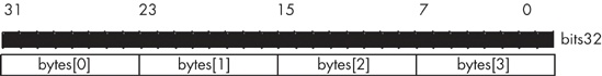
} theValue;This creates the data type shown in Figure 6-14 on a little endian machine and the structure shown in Figure 6-15 on a big endian machine.
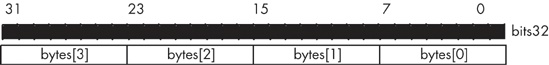
To assemble a 32-bit object from four discrete bytes on a little endian machine, you’d use code like the following:
theValue.bytes[0] = byte0;
theValue.bytes[1] = byte1;
theValue.bytes[2] = byte2;
theValue.bytes[3] = byte3;
This code functions properly because C allocates the first byte of an array at the lowest address in memory (corresponding to bits 0..7 in the theValue.bits32 object on a little endian machine), the second byte of the array follows (bits 8..15), then the third (bits 16..23), and finally the HO byte (occupying the highest address in memory, corresponding to bits 24..31).
However, on a big endian machine, this code won’t work properly because theValue.bytes[0] corresponds to bits 24..31 of the 32-bit value rather than bits 0..7. To assemble this 32-bit value properly on a big endian system, you’d need to use code like the following:
theValue.bytes[0] = byte3;
theValue.bytes[1] = byte2;
theValue.bytes[2] = byte1;
theValue.bytes[3] = byte0;
The only question remaining is, “How do you determine if your code is running on a little endian or big endian machine?” This is actually an easy task to accomplish. Consider the following C code:
theValue.bytes[0] = 0;
theValue.bytes[1] = 1;
theValue.bytes[2] = 0;
theValue.bytes[3] = 0;
isLittleEndian = theValue.bits32 == 256;
On a big endian machine, this code sequence will store the value one into bit 16, producing a 32-bit value that is definitely not equal to 256, whereas on a little endian machine this code will store the value one into bit 8, producing a 32-bit value equal to 256. Therefore, you can test the isLittleEndian variable to determine whether the current machine is little endian (true) or big endian (false).
Although modern computers are quite fast and getting faster all the time, they still require a finite amount of time to accomplish even the smallest tasks. On von Neumann machines, most operations are serialized, which means that the computer executes commands in a prescribed order. It wouldn’t do, in the following code sequence for example, to execute the Pascal statement I := I * 5 + 2; before the statement I := J; finishes:
I := J;
I := I * 5 + 2;
On real computer systems, operations do not occur instantaneously. Moving a copy of J into I takes a certain amount of time. Likewise, multiplying I by five and then adding two and storing the result back into I takes time. A natural question to ask is, “How does the processor execute statements in the proper order?” The answer is, “The system clock.”
The system clock serves as the timing standard within the system, so to understand why certain operations take longer than others, you must first understand the function of the system clock.
The system clock is an electrical signal on the control bus that alternates between zero and one at a periodic rate (see Figure 6-16). All activity within the CPU is synchronized with the edges (rising or falling) of this clock signal.
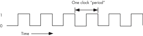
The frequency with which the system clock alternates between zero and one is the system clock frequency and the time it takes for the system clock to switch from zero to one and back to zero is the clock period. One full period is also called a clock cycle. On most modern systems, the system clock switches between zero and one at rates exceeding several billion times per second. A typical Pentium IV chip, circa 2004, runs at speeds of three billion cycles per second or faster. Hertz (Hz) is the unit corresponding to one cycle per second, so the aforementioned Pentium chip runs at between 3,000 and 4,000 million hertz, or 3,000–4,000 megahertz (MHz), also known as 3–4 gigahertz (GHz). Typical frequencies for 80x86 parts range from 5 MHz up to several gigahertz and beyond.
As you may have noticed, the clock period is the reciprocal of the clock frequency. For example, a 1-MHz clock would have a clock period of one microsecond (one millionth of a second). A CPU running at 1 GHz would have a clock period of one nanosecond (ns), or one billionth of a second. We usually express clock periods in millionths or billionths of a second.
To ensure synchronization, most CPUs start an operation on either the falling edge (when the clock goes from one to zero) or the rising edge (when the clock goes from zero to one). The system clock spends most of its time at either zero or one and very little time switching between the two. Therefore, a clock edge is the perfect synchronization point.
Because all CPU operations are synchronized with the clock, the CPU cannot perform tasks any faster than the clock runs. However, just because a CPU is running at some clock frequency doesn’t mean that it executes that many operations each second. Many operations take multiple clock cycles to complete, so the CPU often performs operations at a significantly slower rate.
Memory access is an operation that is synchronized with the system clock. That is, memory access occurs no more often than once every clock cycle. Indeed, on some older processors, it takes several clock cycles to access a memory location. The memory access time is the number of clock cycles between a memory request (read or write) and when the memory operation completes. This is an important value, because longer memory access times result in lower performance.
Modern CPUs are much faster than memory devices, so systems built around these CPUs often use a second clock, the bus clock, which is some fraction of the CPU speed. For example, typical processors in the 100-MHz-to-4-GHz range can use 800-MHz, 500-MHz, 400-MHz, 133-MHz, 100-MHz, or 66-MHz bus clocks (a given CPU generally supports several different bus speeds, and the exact range the CPU supports depends upon that CPU).
When reading from memory, the memory access time is the time between when the CPU places an address on the address bus and the time when the CPU takes the data off the data bus. On typical 80x86 CPUs with a one cycle memory access time, the timing of a read operation looks something like that shown in Figure 6-17. The timing of writing data to memory is similar (see Figure 6-18).

Note that the CPU doesn’t wait for memory. The access time is specified by the bus clock frequency. If the memory subsystem doesn’t work fast enough to keep up with the CPU’s expected access time, the CPU will read garbage data on a memory read operation and will not properly store the data on a memory write. This will surely cause the system to fail.
Memory devices have various ratings, but the two major ones are capacity and speed. Typical dynamic RAM (random access memory) devices have capacities of 512 MB (or more) and speeds of 0.25–100 ns. A typical 3-GHz Pentium system uses 2.0-ns (500-MHz) memory devices.
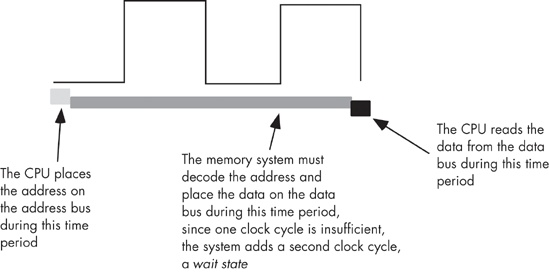
Wait just a second here! Earlier we saw that the memory speed must match the bus speed or the system would fail. At 3 GHz the clock period is roughly 0.33 ns. How can a system designer get away with using 2.0 ns memory? The answer is wait states.
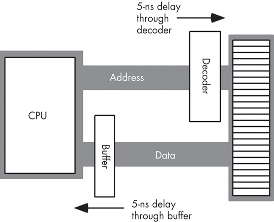
A wait state is an extra clock cycle that gives a device additional time to respond to the CPU. For example, a 100-MHz Pentium system has a 10-ns clock period, implying that you need 10-ns memory. In fact, the implication is that you need even faster memory devices because in most computer systems there is additional decoding and buffering logic between the CPU and memory. This circuitry introduces its own delays. In Figure 6-19, you can see that buffering and decoding costs the system an additional 10 ns. If the CPU needs the data back in 10 ns, the memory must respond in 0 ns (which is impossible).
If cost-effective memory won’t work with a fast processor, how do companies manage to sell fast PCs? One part of the answer is the wait state. For example, if you have a 100-MHz processor with a memory cycle time of 10 ns and you lose 2 ns to buffering and decoding, you’ll need 8-ns memory. What if your system can only support 20-ns memory, though? By adding wait states to extend the memory cycle to 20 ns, you can solve this problem.
Almost every general-purpose CPU in existence provides a pin (whose signal appears on the control bus) that allows the insertion of wait states. If necessary, the memory address decoding circuitry asserts this signal to give the memory sufficient access time (see Figure 6-20).
Needless to say, from the system-performance point of view, wait states are not a good thing. While the CPU is waiting for data from memory, it cannot operate on that data. Adding a wait state typically doubles the amount of time required to access memory. Running with a wait state on every memory access is almost like cutting the processor clock frequency in half. You’re going to get less work done in the same amount of time.
However, we’re not doomed to slow execution because of added wait states. There are several tricks hardware designers can employ to achieve zero wait states most of the time. The most common of these is the use of cache (pronounced “cash”) memory.
If you look at a typical program, you’ll discover that it tends to access the same memory locations repeatedly. Furthermore, you’ll also discover that a program often accesses adjacent memory locations. The technical names given to these phenomena are temporal locality of reference and spatial locality of reference. When exhibiting spatial locality, a program accesses neighboring memory locations within a short period after the initial memory access.
When displaying temporal locality of reference, a program accesses the same memory location repeatedly during a short time. Both forms of locality occur in the following Pascal code segment:
for i := 0 to 10 do
         A [i] := 0;
There are two occurrences each of spatial and temporal locality of reference within this loop. Let’s consider the obvious ones first.
In this Pascal code, the program references the variable i several times. The for loop compares i against 10 to see if the loop is complete. It also increments i by one at the bottom of the loop. The assignment statement also uses i as an array index. This shows temporal locality of reference in action because the CPU accesses i at three points in a short time period.
This program also exhibits spatial locality of reference. The loop itself zeros out the elements of array A by writing a zero to the first location in A, then to the second location in A, and so on. Because Pascal stores the elements of A in consecutive memory locations, each loop iteration accesses adjacent memory locations.
There is an additional example of temporal and spatial locality of reference in this Pascal example. Machine instructions also reside in memory, and the CPU fetches these instructions sequentially from memory and executes these instructions repeatedly, once for each loop iteration.
If you look at the execution profile of a typical program, you’ll discover that the program typically executes less than half the statements. Generally, a program might only use 10 to 20 percent of the memory allotted to it. At any one given time, a 1-MB program might only access 4–8 KB of data and code. So if you paid an outrageous sum of money for expensive zero-wait-state RAM, you would only be using a tiny fraction of it at any one given time. Wouldn’t it be nice if you could buy a small amount of fast RAM and dynamically reassign its addresses as the program executes?
This is exactly what cache memory does for you. Cache memory sits between the CPU and main memory. It is a small amount of very fast memory. Unlike normal memory, the bytes appearing within a cache do not have fixed addresses. Instead, cache memory can dynamically reassign addresses. This allows the system to keep recently accessed values in the cache. Addresses that the CPU has never accessed or hasn’t accessed in some time remain in main (slow) memory. Because most memory accesses are to recently accessed variables (or to locations near a recently accessed location), the data generally appears in cache memory.
A cache hit occurs whenever the CPU accesses memory and finds the data in the cache. In such a case, the CPU can usually access data with zero wait states. A cache miss occurs if the data cannot be found in the cache. In that case, the CPU has to read the data from main memory, incurring a performance loss. To take advantage of temporal locality of reference, the CPU copies data into the cache whenever it accesses an address not present in the cache. Because it is likely the system will access that same location shortly, the system will save wait states on future accesses by having that data in the cache.
Cache memory does not eliminate the need for wait states. Although a program may spend considerable time executing code in one area of memory, eventually it will call a procedure or wander off to some section of code outside cache memory. When that happens, the CPU has to go to main memory to fetch the data. Because main memory is slow, this will require the insertion of wait states. However, once the CPU accesses the data, it is now available in the cache for future use.
We’ve discussed how cache memory handles the temporal aspects of memory access, but not the spatial aspects. Caching memory locations when you access them won’t speed up the program if you constantly access consecutive locations that you’ve never before accessed. To solve this problem, when a cache miss occurs most caching systems will read several consecutive bytes of main memory (engineers call this block of data a cache line). 80x86 CPUs, for example, read between 16 and 64 bytes upon a cache miss. But this brings up an important question. If you read 16 bytes, why read the bytes in blocks rather than as you need them? As it turns out, most memory chips available today have special modes that let you quickly access several consecutive memory locations on the chip. The cache exploits this capability to reduce the average number of wait states needed to access sequential memory locations. Although reading 16 bytes on each cache miss is expensive if you only access a few bytes in the corresponding cache line, cache memory systems work quite well in the average case.
It should come as no surprise that the ratio of cache hits to misses increases with the size (in bytes) of the cache memory subsystem. The 80486 CPU, for example, has 8,192 bytes of on-chip cache. Intel claims to get an 80–95 percent hit rate with this cache (meaning 80–95 percent of the time the CPU finds the data in the cache). This sounds very impressive. However, if you play around with the numbers a little bit, you’ll discover it’s not all that impressive. Suppose we pick the 80 percent figure. This means that one out of every five memory accesses, on the average, will not be in the cache. If you have a 50-MHz processor and a 90-ns memory access time, four out of five memory accesses require only one clock cycle (because they are in the cache) and the fifth will require about ten wait states. Ten wait states were computed as follows: five clock cycles to read the first four bytes (10 + 20 + 20 + 20 + 20 = 90). However, the cache always reads 16 consecutive bytes. Most 80486-era memory subsystems let you read consecutive addresses in about 40 ns after accessing the first location. Therefore, the 80486 will require an additional 6 clock cycles to read the remaining three double words. The total is 11 clock cycles or 10 wait states.
Altogether, the system will require 15 clock cycles to access five memory locations, or 3 clock cycles per access, on the average. That’s equivalent to two wait states added to every memory access. Doesn’t sound so impressive, does it? It gets even worse as you move up to faster processors and the difference in speed between the CPU and memory increases.
There are a couple of ways to improve the situation. First, you can add more cache memory. Alas, you can’t pull an 80486 chip apart and solder more cache onto the chip. However, modern Pentium CPUs have a significantly larger cache than the 80486 and operate with fewer average wait states. This improves the cache hit ratio, reducing the number of wait states. For example, increasing the hit ratio from 80 percent to 90 percent lets you access 10 memory locations in 20 cycles. This reduces the average number of wait states per memory access to one wait state, a substantial improvement.
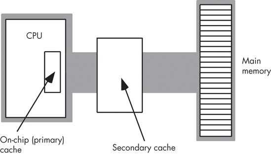
Another way to improve performance is to build a two-level caching system. Many Pentium systems work in this fashion. The first level is the on-chip 8,192-byte cache. The next level, between the on-chip cache and main memory, is a secondary cache often built on the computer system circuit board (see Figure 6-21). However, on newer processors, the first- and second-level caches generally appear in the same packaging as the CPU. This allows the CPU designers to build a higher performance CPU/memory interface, allowing the CPU to move data between caches and the CPU (as well as main memory) much more rapidly.
A typical secondary cache contains anywhere from 32,768 bytes to over 1 MB of memory. Common sizes on PC subsystems are 256 KB, 512 KB, and 1,024 KB (1 MB) of cache.
You might ask, “Why bother with a two-level cache? Why not use a 262,144-byte cache to begin with?” It turns out that the secondary cache generally does not operate at zero wait states. The circuitry to support 262,144 bytes of fast memory would be very expensive, so most system designers use slower memory, which requires one or two wait states. This is still much faster than main memory. Combined with the existing on-chip level-one cache, you can get better performance from the system with a two-level caching system.
Today, you’ll find that some systems incorporate an off-CPU third-level cache. Though the performance improvement afforded by a third-level cache is nowhere near what you get with a first- or second-level cache subsystem, third-level cache subsystems can be quite large (usually several megabytes) and work well for large systems with gigabytes of main memory. For programs that manipulate considerable data, yet exhibit locality of reference, a third-level caching subsystem can be very effective.
Most CPUs have two or three different ways to access memory. The most common memory addressing modes modern CPUs support are direct, indirect, and indexed. A few CPUs (like the 80x86) support additional addressing modes like scaled indexed, while some RISC CPUs only support indirect access to memory. Having additional memory addressing modes makes memory access more flexible. Sometimes a particular addressing mode can allow you to access data in a complex data structure with a single instruction, where two or more instructions would be required on a CPU without that addressing mode. Therefore, having a wide variety of ways to access memory is generally good as these complex addressing modes allow you to use fewer instructions.
It would seem that the 80x86 processor family (with many different types of memory addressing modes) would be more efficient than a RISC processor that only supports a small number of addressing modes. In many respects, this is absolutely true; those RISC processors can often take three to five instructions to do what a single 80x86 instruction does. However, this does not mean that an 80x86 program will run three to five times faster. Don’t forget that access to memory is very slow, usually requiring wait states. Whereas the 80x86 frequently accesses memory, RISC processors rarely do. Therefore, that RISC processor can probably execute the first four instructions, which do not access memory at all, while the single 80x86 instruction, which accesses memory, is spinning on some wait states. In the fifth instruction the RISC CPU might access memory and will incur wait states of its own. If both processors execute an average of one instruction per clock cycle and have to insert 30 wait states for a main memory access, we’re talking about a difference of 31 clock cycles (80x86) versus 35 clock cycles (RISC), only about a 12 percent difference.
If an application must access slow memory, then choosing an appropriate addressing mode will often allow that application to compute the same result with fewer instructions and with fewer memory accesses, thus improving performance. Therefore, understanding how an application can use the different addressing modes a CPU provides is important if you want to write fast and compact code.
The direct addressing mode encodes a variable’s memory address as part of the actual machine instruction that accesses the variable. On the 80x86 for example, direct addresses are 32-bit values appended to the instruction’s encoding. Generally, a program uses the direct addressing mode to access global static variables. Here’s an example of the direct addressing mode in HLA assembly language:
static
    i:dword;
         . . .
    mov( eax, i ); // Store EAX's value into the i variable.
When accessing variables whose memory address is known prior to the execution of the program, the direct addressing mode is ideal. With a single instruction you can reference the memory location associated with the variable. On those CPUs that don’t support a direct addressing mode, you may need an extra instruction (or more) to load a register with the variable’s memory address prior to accessing that variable.
The indirect addressing mode typically uses a register to hold a memory address (there are a few CPUs that use memory locations to hold the indirect address, but this form of indirect addressing is rare in modern CPUs).
There are a couple of advantages of the indirect addressing mode over the direct addressing mode. First, you can modify the value of an indirect address (the value being held in a register) at run time. Second, encoding which register specifies the indirect address takes far fewer bits than encoding a 32-bit (or 64-bit) direct address, so the instructions are smaller. One disadvantage of the indirect addressing mode is that it may take one or more instructions to load a register with an address before you can access that address.
Here is a typical example of a sequence in HLA assembly language that uses an 80x86 indirect addressing mode (brackets around the register name denote the use of indirect addressing):
static
    byteArray: byte[16];
         . . .
    lea( ebx, byteArray );  // Loads EBX register with the address
                            //  of byteArray.
    mov( [ebx], al );       // Loads byteArray[0] into AL.
    inc( ebx );             // Point EBX at the next byte in memory
                            //  (byteArray[1]).
    mov( [ebx], ah );       // Loads byteArray[1] into AH.
The indirect addressing mode is useful for many operations, such as accessing objects referenced by a pointer variable.
The indexed addressing mode combines the direct and indirect addressing modes into a single addressing mode. Specifically, the machine instructions using this addressing mode encode both an offset (direct address) and a register in the bits that make up the instruction. At run time, the CPU computes the sum of these two address components to create an effective address. This addressing mode is great for accessing array elements and for indirect access to objects like structures and records. Though the instruction encoding is usually larger than for the indirect addressing mode, the indexed addressing mode offers the advantage that you can specify an address directly within an instruction without having to use a separate instruction to load the address into a register.
Here is a typical example of a sequence in HLA that uses an 80x86 indexed addressing mode:
static
    byteArray: byte[16];
        . . .
    mov( 0, ebx );                    // Initialize an index into the array.
    while( ebx < 16 ) do

        mov( 0, byteArray[ebx] );     // Zeros out byteArray[ebx].
        inc( ebx );                   // EBX := EBX +1, move on to the
                                      //  next array element.

    endwhile;
The byteArray[ebx] instruction in this short program demonstrates the indexed addressing mode. The effective address is the address of the byteArray variable plus the current value in the EBX register.
To avoid wasting space encoding a 32-bit or 64-bit address into every instruction that uses an indexed addressing mode, many CPUs provide a shorter form that encodes an 8-bit or 16-bit offset as part of the instruction. When using this smaller form, the register provides the base address of the object in memory, and the offset provides a fixed displacement into that data structure in memory. This is useful, for example, when accessing fields of a record or structure in memory via a pointer to that structure. The earlier HLA example encodes the address of byteArray using a 4-byte address. Compare this with the following use of the indexed addressing mode:
lea( ebx, byteArray ); // Loads the address of byteArray into EBX.
    . . .
mov( al, [ebx+2] );    // Stores al into byteArray[2]
This last instruction encodes the displacement value using a single byte (rather than four bytes), hence the instruction is shorter and more efficient.
The scaled indexed addressing mode, available on several CPUs, provides two facilities above and beyond the indexed addressing mode:
The ability to use two registers (plus an offset) to compute the effective address
The ability to multiply one of those two registers’ values by a common constant (typically 1, 2, 4, or 8) prior to computing the effective address.
This addressing mode is especially useful for accessing elements of arrays whose element sizes match one of the scaling constants (see the discussion of arrays in the next chapter for the reasons).
The 80x86 provides a scaled index addressing mode that takes one of several forms, as shown in the following HLA statements:
mov( [ebx+ecx*1], al );             // EBX is base address, ecx is index.
mov( wordArray[ecx*2], ax );        // wordArray is base address, ecx is index.
mov( dwordArray[ebx+ecx*4], eax );  // Effective address is combination
// of offset(dwordArray)+ebx+(ecx*4).This chapter has spent considerable time discussing how the CPU organizes memory and how the CPU accesses memory. There are a couple of good sources of additional information on this subject.
My book The Art of Assembly Language (No Starch Press), or nearly any other textbook on assembly language programming, will provide additional information about CPU addressing modes, allocating and accessing local (automatic) variables, and manipulating parameters at the machine code level. Any decent textbook on programming language design or compiler design will have lots to say about the run-time organization of memory for typical compiled languages.
A good computer architecture textbook is another place you’ll find information on system organization. Patterson and Hennessy’s architecture books Computer Organization & Design: The Hardware/Software Interface and Computer Architecture: A Quantitative Approach are well-regarded textbooks you might consider reading to gain a more in-depth perspective on CPU and system design.
Chapter 11 in this book also provides additional information about cache memory and memory architecture.
[29] 680x0 series processors starting with the 68020, found in later Macintosh systems, corrected this and allowed data access of words and double words at arbitrary addresses.