
CONTENTS
3.2 The Statistical 3D Device Simulation
Silicon device technology scaling and performance improvement require [1, 2 and 3] not only overcoming a variety of fabrication challenges but also suppressing systematic variation and random effects [4, 5, 6 and 7]. Except process variation effect (PVE), random dopant fluctuation (RDF), as one of the known major intrinsic parameter fluctuations, complicates device manufacturing and degrades device characteristics in the nanometer scale complementary metal–oxide semiconductor (nano-CMOS) device era [8, 9, 10, 11, 12, 13, 14, 15, 16, 17, 18, 19, 20, 21, 22, 23, 24, 25, 26, 27, 28, 29 and 30]. High-κ/metal-gate (HKMG) technology has been a key way to suppress RDF-induced variability and reduce leakage current [31, 32, 33, 34, 35, 36, 37 and 38]; however, HKMG may introduce random interface traps (ITs) at a high-κ/silicon interface and such IT fluctuation (ITF) degrades device characteristics considerably [39, 40, 41, 42, 43, 44, 45, 46 and 47]. Various simulations of the device’s variability induced by ITF were reported by using a one-dimensional (1D) IT’s model for sub-65-nm CMOS devices [46], a 2D IT’s model for 16-nm-gate HKMG devices [39], local interaction of the combined RDs and ITs [40,41], and full fluctuation among all random sources [4]. Recently, the asymmetric RDF on device characteristics was studied for 16-nm-gate HKMG metal–oxide–semiconductor field effect transistor (MOSFET) devices [48,49]. However, induced by random ITs, asymmetric physical and electrical characteristic fluctuations of 16-nm-gate HKMG MOSFETs have not been discussed yet.
In this chapter, the asymmetric characteristic fluctuation of the random ITs in 16-nm-gate HKMG MOSFETs is presented. Random ITs at the 2D interface of the hafnium oxide (HfO2)/silicon of the 16-nm-gate HKMG N-MOSFETs are incorporated into an experimentally validated 3D device simulation [11] to quantify the random ITs-fluctuated characteristics. Large-scale statistical 3D device simulation is performed by solving a set of calibrated 3D electron–hole density-gradient equations coupling with the Poisson equation as well as electron–hole current continuity equations [50,51]. On the basis of the large-scale statistical 3D device simulation of random ITs-fluctuated samples, the random ITs-induced threshold voltage fluctuation and on-/off-state current fluctuation are estimated and compared with other significant fluctuation sources. In particular, an asymmetric drain-induced, barrier-lowering fluctuation σDIBL and a subthreshold swing fluctuation σSS [1] are studied by classifying the random ITs into the regions near the source side, around the middle of the channel, and near the drain side of the silicon channel, respectively. Our quantum mechanically corrected device simulation was compared with experimental data aiming at the greatest accuracy [11], which further enables us to explore both the individual and combined effects of randomly existing ITs and RDs on device characteristics in a unified way. The random 2D ITs are also solved with 3D RDs inside the silicon channel at the same time to assess the interaction effect of the combined ITs and RDs. For the studied 16-nm-gate HKMG N-MOSFETs with a device width of 16 nm, the high density of ITs (Dit) in the range of 3 × 10¹¹−3.3 × 10¹² eV−1cm−2 results in 26.3 mV fluctuation of threshold voltage and for the low Dit varying from 2.5 × 10¹⁰ to 3.8 × 10¹¹ eV−1cm−2. Both the high and low Dit-induced are smaller than that of . The largest asymmetric values of σVth and σSS are observed when random ITs with high Dit are near the source side, compared with the random ITs located at the middle of the channel and near the drain side. The engineering findings of this study indicate that both the ITs near the source side of the silicon channel and the RDs near the channel surface possess the largest characteristic fluctuations.
This chapter is organized as follows. In Section 3.2, we describe the simulation settings for random ITs-, RDs-, and the combined ITs and RDs (denoted as “ITs + RDs”)-induced device and circuit’s characteristic fluctuations. In Section 3.3, we discuss the findings of this study for the random ITs-fluctuated 16-nm-gate devices as well as the static random-access memory (SRAM). Finally, we draw conclusions and suggest future work.
3.2 THE STATISTICAL 3D DEVICE SIMULATION
The devices we examined are the 16-nm-gate titanium-nitride (TiN) gate MOSFETs with an amorphous-based TiN/HfO2 gate stack which has an effective oxide thickness (EOT) of 0.8 nm, as shown in Figure 3.1a. The EOT varying from 0.4 to 1.2 nm will also be simulated for examining the impact of different high-κ gate stacks on fluctuation suppression. Note that the device’s width is equal to the gate length of 16 nm, which is designed for the most critical assessment. The validated nominal device characteristics of the studied 16-nm-gate HKMG MOSFETs are calibrated, where the magnitude of the threshold voltages of the 16-nm-gate N- and P-MOSFETs is 250 mV. To examine the asymmetric characteristic fluctuation induced by random ITs, as shown in Figure 3.1a, we have partitioned the channel into three different regions: random ITs near the source side, around the middle of the channel, and near the drain side.
To carry out the statistical 3D device simulation with random ITs at HfO2/Si interface, we first randomly generate 753 acceptor-like ITs (gray dots), as shown in Figure 3.1b, in a large 2D plane of (224 nm)2 where the random ITs’ concentration is around 1.5 × 1012 cm−2 in the large plane. Notably, this value is mainly for statistically generating the number of random ITs, which is not equal to the effective entire density of ITs (Dit). The total number of generated random ITs follows the Poisson distribution [1,42, 43, 44, 45, 46 and 47]. The large plane is then partitioned into many subplanes, where the size of each subplane is 16 nm2. The number of random ITs in each subplane varies from 1 to 8 and the average number of ITs is 4, as shown in the histogram bar chart of Figure 3.1b. Each IT’s energy on a subplane is randomly assigned according to the relation of Dit versus the energy [1,42, 43, 44, 45, 46 and 47], as shown in Figure 3.1b; consequently, each IT’s density can be estimated according to its randomly assigned energy and the Dit may vary randomly from 1 × 10¹⁰ to 1 × 10¹² eV−1 cm−2, which quantitatively coincides with our experimental characterization for sub-20-nm HKMG CMOS devices. We repeat this process until all subregions are assigned. Therefore, 196 randomly generated 3D device samples with 2D random ITs at the HfO2/Si interface are simulated to assess the influence of ITF.
For the RDF simulation, we mainly follow the simulation procedure reported in our recent work [4,8, 9, 10, 11, 12 and 13]. As shown in Figure 3.1c, the RDs in the 3D device channel region are statistically incorporated into the statistical 3D device simulation running on our parallel computing system [52]. Note that, for the best accuracy of our computational model, the implemented statistical 3D device simulation technique for estimating characteristic fluctuation was experimentally validated with silicon data for sub-20-nm devices in our earlier work [11], where the RDs-fluctuated mobility was validated with experimentally measured current–voltage (I–V) data. To compare with other significant fluctuation sources, such as PVE, oxide thickness fluctuation (OTF), and work function fluctuation (WKF) with different sized TiN grain, we follow the simulation procedures reported in our recent work [4].
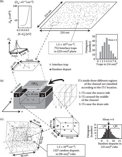
FIGURE 3.1 (a) Illustration of the studied device together with two sources of randomness: interface traps (gray dots) located at the HfO2/Si interface and random dopants (dark dots) located at the silicon channel. Interface traps (ITs) inside three different regions of the channel are classified according to the ITs’ location. They are, ITs near the source side, ITs around the middle of the channel and ITs near the drain side. Statistical 3D device simulation settings for the characteristic fluctuation resulting from random ITs and random dopants (RDs) are shown in (b) and (c). (b) We first generate 753 acceptor-like traps in a large plane for the 16-nm-gate N-MOSFET devices, where the IT’s concentration at the large plane of (224 nm)2 is around 1.5 × 1012 cm−2 and the total number of generated ITs follows the Poisson distribution. Each IT’s energy on the plane is independently assigned according to the distribution of its density. Then, the entire plane is partitioned into many subplanes of (16 nm)2 corresponding to the device’s size, where the number of ITs in each subplane may vary from 1 to 8 and the average number is 4. Thus, the effective density of interface traps (Dit) varies from 3 × 10¹¹ to 3.3 × 10¹² eV−1cm−2. We call the ITs with high Dit for device Dit ranging from 3 × 10¹¹ to 3.3 × 10¹² eV−1 cm−2 and the ITs with low Dit for device Dit ranging from 2.5 × 10¹⁰ to 3.8 × 10¹¹ eV−1cm−2. (c) For the setting of discrete dopants, impurities are randomly generated and distributed in a (96 nm)3 cube with an average concentration of 1.5 × 1018 cm−3. There will be 1327 discrete dopants within the cube, and the number of discrete dopants varies from 0 to 14 (the average number is six) for all 216 subcubes of (16 nm)3, which corresponds to the volume of the studied devices. Consequently, the total subcubes and subplanes can be mapped into the device’s 3D channel and 2D surface for the characteristic fluctuation induced by the ITs, RDs, and combined ITs and RDs, respectively.
The statistically generated ITs are further implemented for 16-nm-gate P-MOSFET devices so that the 16-nm-gate CMOS SRAM circuit can be simulated using coupled device–circuit solution methodology [13] to estimate the transfer characteristic fluctuation at the circuit level, as shown in Figure 3.2a. The computational flow of the coupled device–circuit simulation is shown in Figure 3.2b. Owing to the lack of well-established compact models for the 16-nm-gate CMOS devices, by using the coupled device–circuit simulation technique, the circuit-level fluctuations are estimated for the CMOS SRAM circuit, as shown in Figure 3.2a. To estimate the SRAM’s static noise margin fluctuation σSNM, electrical characteristics of each randomly generated device in the tested circuit are first calculated by the 3D device simulation. The obtained result is then used as the devices’ terminal characteristics in the coupled device–circuit steady-state simulation. The nodal equations of the tested SRAM circuit are formulated and then directly coupled to the device transport equations (in the form of a large matrix that contains both circuit and device equations), which are solved simultaneously to obtain the circuit transfer characteristics. The device characteristics obtained by device simulation, such as the distributions of potential and current density, are input in the SRAM circuit simulation through the device’s contact terminals. Notably, to explore the influence of the intrinsic parameter fluctuation of σSNM of the SRAM circuit, the random samples are generated and performed, respectively.
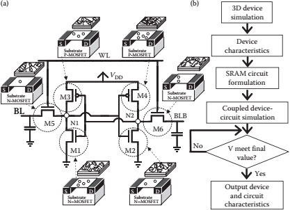
FIGURE 3.2 (a) To calculate the σSNM, the totally random generated N- and P-MOSFET devices with different random sources are assigned into the 6T SRAM circuit for the coupled device-circuit simulation. (b) The proposed flowchart for the coupled device-circuit simulation. Notably, the voltage of node N2(V) in the simulated 6T SRAM circuit is applied to 0.8 V. To assess the worst influences of ITs, RDs, and combined ITs and RDs on the 16-nm-gate SRAM’s transfer characteristics, the cell ratio is set to 1 for all simulations.
First, we explore the random ITs-fluctuated terminal current; Figure 3.3a shows the totally random ITs-induced fluctuations of drain current–gate voltage (ID–VG) curves of the 16-nm-gate N-MOSFETs with high Dit, where the line with circles indicates the nominal case and all dashed lines are the random ITs-fluctuated cases. The nominal case is the fresh device without random ITs. The random ITs located at the HfO2/silicon interface may destroy the screening effect and the threshold voltage is simply raised. As shown in Figure 3.3b, the value of threshold voltage is determined from a constant current criterion when the drain current is greater than 10−7 × (W/L) A, where L and W are the gate length and device width, respectively. The threshold voltage increases, and then the on-/off-state current (Ion/Ioff) decreases accordingly, as the number of random ITs increases. The simulated is 26.3 mV, which is smaller than the result of RDF . The random ITs-position induced different fluctuations of characteristics in spite of having the same number of ITs, as marked by an open bar in the inset of Figure 3.3b, where the magnitude of the spread characteristics of the threshold voltage increases as the number of random ITs increases. Figures 3.3b and c show the extracted Ion and Ioff as functions of the number of random ITs, where each symbol shows each random IT-fluctuated result. The magnitude of each random ITs-fluctuated current decreases as the number of random ITs increases. Similarly, the random ITs-position induced rather different current fluctuations in spite of having the same number of random ITs, as marked by an open bar in insets of Figures 3.3c and d. To explore the impact of the random position of ITs on the device’s physical characteristics, as shown in Figure 3.4, the random ITs-fluctuated surface potential and the electron current density from the source side to the drain side for the device at the on-state condition are further discussed. Three cases are selected among 196 simulations to demonstrate the random position associated local repulsive Coulomb field and disturbed electron current conducting path at the HfO2/Si interface. Figure 3.4a shows the plots for the case of the random 4 ITs near the source side. Compared with the random ITs appearing in the other two regions, as shown in Figures 3.4b and c, the distribution of electron current density is seriously destroyed because of the random 4 ITs near the source side locally, which results in a relatively higher local spike of potential barriers and thus raises the threshold voltage (Vth = 316 mV). Figures 3.4b and c show plots for the case of the random 4 ITs around the middle of the channel and for the case of the random 4 ITs near the drain side. These random 4 ITs positioning away from the source side have relatively weakened local spikes of potential barriers which still effectively impede electron current conduction; however, they are weaker than that of the random 4 ITs appearing in the source side, as shown in Figure 3.4a. Thus, the device with random ITs of Figure 3.4c has minimal threshold voltage (Vth = 257 mV) and the largest area of electron current conduction, compared with the case of Figure 3.4a. The asymmetric impact of random ITs on the surface potential results in quite different threshold voltage as well as the variance of the threshold voltage, as listed in Table 3.1. The statistically simulated ID − VG curves enable us to extract the σVth, induced by different sources of fluctuations among different regions. As listed in Table 3.1, the ITF induced-σVth, and σSS for the device with random ITs near the source side, around the middle of the channel, and near the drain side, respectively, are further calculated and classified. The studied 16-nm-gate N-MOSFETs with both the high and low Dit of ITs are simulated; significant values of σVth, and σSS induced by random ITs with high Dit near the source side are observed, compared with the random ITs located at the middle of the channel and near the drain side. However, the simulation indicates that there is no differences in σVth, and σSS for the cases of random ITs located at the middle of the channel and near the drain side. In particular, for a device with a low Dit, near the source side, the σVth, is reduced from 28.7 to 10.2 mV; similarly, the σSS is reduced from 21.2 to 5.6 mV/Dec. The impact of RDs on the threshold voltage, SS, and DIBL, among the aforementioned three regions is insignificant, but the impact of RDs near the channel surface is different from RDs located away from the depletion region of the channel [8, 9, 10, 11, 12 and 13,48,49].
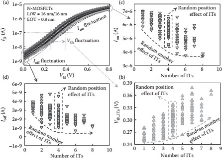
FIGURE 3.3 (a) The plot of ITs-fluctuated ID–VG curves shows the random ITs-induced DC characteristic fluctuations for the studied devices. The line with circles is the nominal case calibrated to Vth = 250 mV and others are the random ITs-fluctuated cases. From the ID–VG curve, we can extract the threshold voltage fluctuation, the off-state current fluctuation, and the on-state current fluctuation with respect to the number of ITs, as shown in (b), (c), and (d), respectively. We observe that the threshold voltage is increased, and thus the off-state current and the on-state current are decreased as the number of ITs is increased due to the relatively higher barriers generated. Except for the random number effect of ITs, the random position effect of ITs results in different threshold voltage for the same number of ITs.
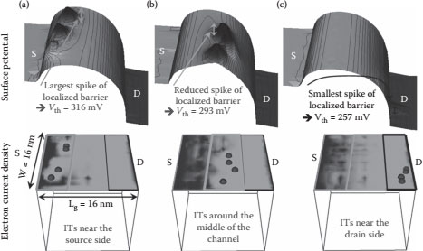
FIGURE 3.4 Plots of the ITs-fluctuated surface potential and the electron current density from the source side to the drain side for the device at the on-state condition. (a) Plots for the case of ITs near the source side. (b) Plots for the case of ITs around the middle of the channel. (c) Plots for the case of ITs near the drain side. The asymmetric impact of ITs on the surface potential results in different threshold voltage as well as a variance in the threshold voltage, as listed in Table 3.1.
TABLE 3.1
The ITF Induced and σSS for Device with ITs Near the Source Side, around the Middle of the Channel, and Near the Drain Side, Respectively
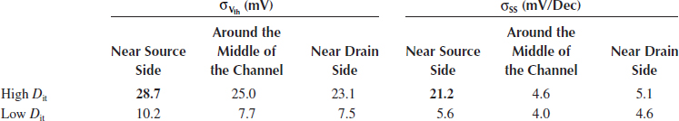
Note: The studied 16-nm-gate N-MOSFETs are with high and low Dit of ITs. Significant values of and σSS induced by random ITs near the source side are observed, compared with the ITs located at the middle of the channel and near the drain side.
The random ITs-fluctuated DIBL effect is pronounced for the 16-nm-gate N-MOSFETs, as shown in Figure 3.5a. For the device at the weak inversion region, there is a potential barrier at the channel region owing to a balance between the drift current and diffusion current. The barrier height decreases as the drain voltage increases; it thus results in an increased drain current, which is controlled not only by the gate voltage but also by the drain voltage. The DIBL effect could be observed through the ID − VG curves of a device under the linear (VD = 0.05 V) and saturated (VD = 0.8 V) regions. It can be calculated by the lateral shift of threshold voltage divided by the difference of the drain voltage and is given in units (mV/V). Figure 3.5a shows the random ITs-fluctuated DIBL characteristic of the 16-nm-gate N-MOSFETs; the magnitude of DIBL decreases as the number of random ITs increases because the random ITs reduce the probability of electric-field lines penetrating from the drain side to the source side. The tendency of increasing fluctuation of DIBL follows the threshold voltage as the number of random ITs increases, as shown in Figure 3.3b. Figure 3.5b shows that the device with a high Dit of random ITs near the source side has a large DIBL at the same number of random ITs; Figure 3.5c shows the device with a high Dit of random ITs around the middle of the channel which has a small DIBL at the same number of random ITs. The random position effect of ITs on the Vth, DIBL, SS strongly depends on the random ITs near the source side. Such asymmetric fluctuation was also observed for devices with RDF [48,49].
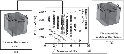
FIGURE 3.5 (a) The drain-induced barrier lowering (DIBL) versus the number of ITs. (b) Device with a high Dit of ITs near the source side has high DIBL at the same number of ITs. (c) Device with a high Dit of ITs around the middle of the channel has low DIBL at the same number of ITs.
We now turn to compare the ITs, RDs, and “ITs + RDs”-induced , of the studied 16-nm-gate N-MOSFETs. Figure 3.6 is the , as a function of EOT with respect to different fluctuation sources: ITs (with high Dit), RDs, and “ITs + RDs.” The device with EOT = 0.8 nm exhibits , , and . We note that is smaller than the result calculated by in which the random variables following statistically independent identical distribution (iid) is assumed. However, the iid assumption on the random variables of Vth,ITs and Vth,RDs is not always true owing to the local interaction of surface potentials at different extents between ITs and RDs concurrently existing in the surface/channel region of the N-MOSFETs. The relative error between and is about 11% overestimation, compared with the of the N-MOSFETs; similarly, not shown here, the studied 16-nm-gate P-MOSFETs has 45 1 mV which is smaller than the statistical sum . Owing to the sizable threshold voltage fluctuation with respect to EOT nonlinearly, the statistical sums of the variances of two random variables induced by ITs and RDs disclose significant errors, compared with the statistical 3D device simulation together with the combined ITs and RDs simultaneously. This investigation shows that the local interaction of surface potentials owing to “ITs + RDs” could not be calculated independently by using the results of ITs and RDs. It explains why the iid assumption overestimates the threshold voltage fluctuations induced by the combined ITs and RDs. As shown in Figure 3.7, the threshold voltage fluctuation induced by various random sources for the 16-nm-gate N-MOSFETs, respectively, are compared. Among the five fluctuation sources, the RDF still dominates the and the PVE plays a sizable fluctuation source; both should be minimized by process innovation continuously. The WKF-induced , is reduced from 36.7 to 11.1 mV when the minimal grain size of the TiN gate is reduced from (4 nm)2 to (2 nm)2. The ITF-induced , is reduced from 26.3 to 10.2 mV when the Dit is reduced from an order of 1012 to 1011 eV−1cm−2. We estimate the σSNM of the 6T SRAM circuit [53], as shown in Figure 3.2a. Butterfly curves fluctuation induced by RDF, PVE, WKF, and ITF of the tested 6T SRAM in read operation is first simulated, where the cell ratio CR = ((W/L) driver transistors:M1 and M2/(W/L)access transistors:M5 and M6) of the SRAM cell in this study is set as unitary, and the nominal value of SNM is 86 mV. They are then used to calculate σSNM with respect to different fluctuation sources, as listed in Table 3.2. The relation between the device transconductance and SNM of SRAM can be viewed as , where Inx is the saturation drain current of the driver transistor of SRAM and Iax is the saturation drain current of the access transistor. The σSNM is directly proportional to the fluctuation of transconductance and the fluctuation of transconductance is influenced by the . Thus, σSNM induced by random ITs with high Dit has a minimal value of 19.1 mV because the is the lowest one among RDF, PVE, and WKF. However, the magnitude of σSNM for all RDF, PVE, WKF, and ITF is up to 20% of the nominal SNM, which may degrade the operation of 6T SRAM and should be improved by using multiple gate FETs or 8T SRAM cells [53].
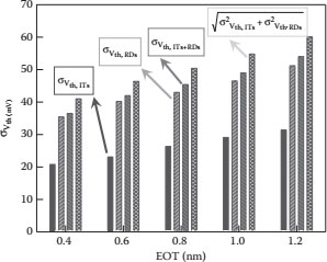
FIGURE 3.6 as a function of EOT with respect to different fluctuation sources: ITs (with high Dit), RDs, and combined ITs and RDs (denoted as “ITs + RDs”). On the basis of the assumption of statistically independent identical distribution to the random variables of ITs and RDs, the is also calculated. Owing to the gate capacitance variation and surface potential interaction at different extents, resulting from combined ITs and RDs, the full 3D simulated is smaller than the result of .
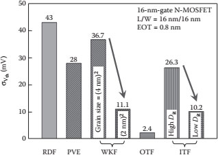
FIGURE 3.7 The threshold voltage fluctuation induced by various random sources for the 16-nm-gate N-MOSFETs. The WKF-induced is reduced from 36.7 mV to 11.1 mV when the grain size of the metal gate is reduced from (4 nm)2 to (2 nm)2. The ITF-induced is reduced from 26.3 mV to 10.2 mV when the effective density of the interface traps is reduced from high Dit to low Dit. Among fluctuations, the RDF dominates the continuously and the PVE should be minimized.
TABLE 3.2
Summarized Static Noise Margin Fluctuation (σSNM) of 16-nm-gate SRAM Induced by RDF, PVE, WKF, and ITF, Respectively
Fluctuation Sources |
RDF |
PVE |
WKF (Grain Size: 4 nm2) |
ITF (with High Dit) |
σSNM (mV) |
27.4 |
20.8 |
25.3 |
19.1 |
Note: σSNM induced by WKF is with 4-nm metal grains and the σSNM induced by ITF is with high Dit.
In this chapter, the asymmetric characteristic fluctuation of the random ITs in 16-nm-gate HKMG MOSFETs has been presented. The random ITs-induced threshold voltage fluctuation and on-/off-state current fluctuation, drain-induced barrier-lowering fluctuation, and subthreshold swing fluctuation have been studied by classifying the random ITs into the regions near the source side, around the middle of the channel, and near the drain side of the silicon channel, respectively. For the studied 16-nm-gate HKMG N-MOSFETs with the device width of 16 nm, both high and low Dit-induced are smaller than that of . The largest asymmetric values of and σSS have been observed when random ITs with high Dit are near the source side, compared with the random ITs located at the middle of the channel and near the drain side. The engineering findings of this study indicate that both the ITs near the source side of the silicon channel and RDs near the channel surface possess the largest characteristic fluctuations. The random ITs have also exhibited sizable σSNM of the 16-nm-gate 6T SRAM circuit, compared with the σSNM induced by RDF, PVE, and WKF.
This work was supported in part by the National Science Council (NSC), Taiwan, under contract no. NSC 101-2221-E-009-092 and by TSMC, Hsinchu, Taiwan, under a 2011–2013 grant.
1. S. M. Sze, Physics of Semiconductor Devices, 2nd Ed., New York, NY: John Wiley and Sons, 1981.
2. G. Moore, Progress in digital integrated electronics, in IEDM Tech. Dig., 11–13, 1975.
3. International Technology Roadmap for Semiconductors [Online]. Available: http://www.itrs.net/
4. Y. Li, C.-H. Hwang, T.-Y. Li, and M.-H. Han, Process-variation effect, metal-gate work-function fluctuation, and random-dopant fluctuation in emerging CMOS technologies, IEEE Trans. Electron Dev., 57(2), 437–447, 2010.
5. Y. Li, H.-W. Cheng, Y.-Y. Chiu, C.-Y. Yiu, and H.-W. Su, A unified 3D device simulation of random dopant, interface trap and work function fluctuations on high-κ/metal gate device, in IEDM Tech. Dig., p. 5–5, 2011.
6. H.-W. Cheng, F.-H. Li, M.-H. Han, C.-Y. Yiu, C.-H. Yu, K.-F. Lee, and Y. Li, 3D device simulation of work-function and interface trap fluctuations on high-κ/metal gate devices, in IEDM Tech. Dig., pp. 379–382, 2010.
7. K. J. Kuhn, M. D. Giles, D. Becher, P. Kolar, A. Kornfeld, R. Kotlyar, S. T. Ma, A. Maheshwari, and S. Mudanai, Process technology variation, IEEE Trans. Electron Dev., 58(8), 2197–2208, 2011.
8. Y. Li, C.-H. Hwang, and T.-Y. Li, Random-dopant-induced device variability in nano-CMOS and digital circuits, IEEE Trans. Electron Dev., 56(8), 1588–1597, 2009.
9. Y. Li, C.-H. Hwang, and T.-Y. Li, Discrete-dopant-induced timing fluctuation and suppression in nanoscale CMOS circuit, IEEE Trans. Circuits and Systems Part II: Express Briefs, 56(5), 379–383, 2009.
10. Y. Li, C.-H. Hwang, and T.-Y. Li, Random-dopant-induced variability in nano-CMOS devices and digital circuits, IEEE Trans. Electron Dev., 56(8), 1588–1597, 2009.
11. Y. Li, S.-M. Yu, J.-R. Hwang, and F.-L. Yang, Discrete dopant fluctuated 20 nm/15 nm-gate planar CMOS, IEEE Trans. Electron Dev., 55(6), 1449–1455, 2008.
12. Y. Li, C.-H. Hwang, and H.-M. Huang, Large-scale atomistic approach to discrete-dopant-induced characteristic fluctuations in silicon nanowire transistors, Phys. Stat. Sol. (a), 205(6), 1505–1510, 2008.
13. Y. Li and C.-H. Hwang, High-frequency characteristic fluctuations of nano-MOSFET circuit induced by random dopants, IEEE Trans. Microwave Theory Tech., 56(12), 2726–2733, 2008.
14. J. Jaffari and M. Anis, Variability-aware bulk-MOS device design, IEEE Trans. CAD Integrated Circuits Systems, 27(2), 205–216, 2008.
15. Y. Li and C.-H. Hwang, Discrete-dopant-induced characteristic fluctuations in 16 nm multiple-gate silicon-on-insulator devices, J. Appl. Phys., 102(8), 084509, 2007.
16. Y. Li and S.-M. Yu, A coupled-simulation-and-optimization approach to nanodevice fabrication with minimization of electrical characteristics fluctuation, IEEE Trans. Semi. Manuf., 20(4), 432–438, 2007.
17. N. Sano and M. Tomizawa, Random dopant model for three-dimensional drift-diffusion simulations in metal-oxide-semiconductor field-effect-transistors, Appl. Phys. Lett., 79, 2267, 2007.
18. T. Ohtou, N. Sugii, and T. Hiramoto, Impact of parameter variations and random dopant fluctuations on short-channel fully depleted SOI MOSFETs with extremely thin BOX, IEEE Electron Dev. Lett., 28(8), 740–742, 2007.
19. Y. Li and S.-M. Yu, Comparison of random-dopant-induced threshold voltage fluctuation in nanoscale single-, double-, and surrounding-gate field-effect transistors, Jpn. J. Appl. Phys., 45(9A), 6860–6865, 2006.
20. C.L. Alexander, G. Roy, and A. Asenov, Random impurity scattering induced variability in conventional nano-scaled MOSFETs: Ab initio impurity scattering Monte Carlo simulation study, in IEDM Tech. Dig., pp. 949–952, 2006.
21. H. Mahmoodi, S. Mukhopadhyay, and K. Roy, Estimation of delay variations due to random-dopant fluctuations in nanoscale CMOS circuits, IEEE J. Solid-State Circuits, 40(9), 1787–1796, 2005.
22. P. Dollfus, A. Bournel, S. Galdin, S. Barraud, and P. Hesto, Effect of discrete impurities on electron transport in ultrashort MOSFET using 3D MC simulation, IEEE Trans. Electron Dev., 51(5), 749–756, May 2004.
23. A. Balasubramanian, P.R. Fleming, B.L. Bhuva, A.L. Sternberg, and L.W. Massengill, Implications of dopant-fluctuation-induced Vt variations on the radiation hardness of deep submicrometer CMOS SRAMs, IEEE Trans. Dev. Mater. Reliab., 8(1), 135–144, 2003.
24. N. Sano, K. Matsuzawa, M. Mukai, and N. Nakayama, On discrete random dopant modeling in drift-diffusion simulations: Physical meaning of “atomistic” dopants, Microelectron. Reliab., 42(2), 189–199, 2002.
25. N. Sano, K. Matsuzawa, M. Mukai, and N. Nakayama, Role of long-range and short-range Coulomb potentials in threshold characteristics under discrete dopants in sub-0.1 μm Si-MOSFETs, in IEDM Tech. Dig., pp. 275–278, Dec. 2000.
26. H.-S. Wong, Y. Taur, and D. J. Frank, Discrete random dopant distribution effects in nanometer-scale MOSFETs, Microelectron. Reliab., 38(9), 1447–1456, 1999.
27. P.A. Stolk, F.P. Widdershoven, and D.B.M. Klaassen, Modeling statistical dopant fluctuations in MOS transistors, IEEE Trans. Electron Dev., 45(9), 1960–1971, 1998.
28. X.-H. Tang, V. K. De, and J.D. Meindl, Intrinsic MOSFET parameter fluctuations due to random dopant placement, IEEE Trans. VLSI Systems, 5(4), 369–376, 1997.
29. J.-R. Zhou and D.K. Ferry, 3D simulation of deep-submicron devices. How impurity atoms affect conductance, IEEE Comput. Sci. Eng., 2(2), 30–37, 1995.
30. R. W. Keyes, Effect of randomness in distribution of impurity atoms on FET thresholds, Appl. Phys., 8, 251–259, 1975.
31. Y. Li and H.-W. Cheng, Random work function induced threshold voltage fluctuation in metal-gate MOS devices by Monte Carlo simulation, IEEE Trans. Semicond. Manuf., 25(2), 266–271, 2012.
32. Y. Li and H.-W. Cheng, Nanosized-metal-grain-induced characteristic fluctuation in 16-nm-gate complementary metal-oxide-semiconductor devices and digital circuits, Jpn. J. Appl. Phys., 50(4), 04DC22, 2011.
33. K. Ohmori, T. Matsuki, D. Ishikawa, T. Morooka, T. Aminaka, Y. Sugita, T. Chikyow, K. Shiraishi, Y. Nara, and K. Yamada, Impact of additional factors in threshold voltage variability of metal/high-κ gate stacks and its reduction by controlling crystalline structure and grain size in the metal gates, in IEDM Tech. Dig., pp. 1–4, Dec. 2008.
34. H. Dadgour, De Vivek, and K. Banerjee, Statistical modeling of metal-gate work-function variability in emerging device technologies and implications for circuit design, in Proc. ICCAD, pp. 270–277, 2008.
35. H. Daewon, H. Takeuchi, Y.-K. Choi, and T.-J. King, Molybdenum gate technology for ultrathin-body MOSFETs and FinFETs, IEEE Trans. Electron Devices, 51, 1989–1996, 2004.
36. A. Yagishita, T. Saito, K. Nakajima, S. Inumiya, K. Matsuo, T. Shibata, Y. Tsunashima, K. Suguro, and T. Arikado, Improvement of threshold voltage deviation in damascene metal-gate transistors, IEEE Trans. Electron Dev., 48, 1604–1611, 2001.
37. J. L. He, Y. Setsuhara, I. Shimizu, and S. Miyake, Structure refinement and hardness enhancement of titanium nitride films by addition of copper, Surf. Coat. Technol., 137, 38–42, 2001.
38. S. Berge, P. O. Gartland, and B. J. Slagsvold, Photoelectric work-function of a molybdenum single crystal for the (100), (110), (111), (112), (114), and (332) faces, Surf. Sci., 43, 275–292, 1974.
39. Y. Li and H.-W. Cheng, Random interface-traps-induced electrical characteristic fluctuation in 16-nm-gate high-κ/metal gate complementary metal-oxide-semiconductor device and inverter circuit, Jpn. J. Appl. Phys., 51(4), 04DC08, 2012.
40. Y. Li, H.-W. Cheng, and Y.-Y. Chiu, Interface traps and random dopants induced characteristic fluctuations in emerging MOSFETs, Microelectron. Eng., 88(7), 1269–1271, 2011.
41. N. Ashraf, D. Vasileska, G. Wirth, and P. Srinivasan, Accurate model for the threshold voltage fluctuation estimation in 45-nm channel length MOSFET devices in the presence of random traps and random dopants, IEEE Electron Dev. Lett., 32(8), 1044–1046, 2011.
42. O. Engström, Electron states in MOS systems, ECS Trans., 35(4), 19–38, 2011.
43. M. Cassé1, K. Tachi1, S. Thiele1, and T. Ernst, Spectroscopic charge pumping in Si nanowire transistors with a high-κ/metal gate, Appl. Phys. Lett., 96, 123506, 2010.
44. A. Appaswamy, P. Chakraborty, and J. Cressler, Influence of interface traps on the temperature sensitivity of MOSFET drain-current variations, IEEE Electron Dev. Lett., 31(5), 387–389, 2010.
45. Md. Mahbub Satter and A. Haque, Modeling effects of interface trap states on the gate C-V characteristics of MOS devices on alternative high-mobility substrates, Solid-State Electron., 54(6), 621–627, 2010.
46. P. Andricciola, H.P. Tuinhout, B. De Vries, N.A.H. Wils, A.J. Scholten, and D.B.M. Klaassen, Impact of interface states on MOS transistor mismatch, in IEDM Tech. Dig., pp. 711–714, 2009.
47. P. K. Hurley, K. Cherkaoui, S. McDonnell, G. Hughes, and A.W. Groenland, Characterisation and passivation of interface defects in (100)-Si/SiO2/HfO2/TiN gate stacks, Microelectron. Reliab., 47(8), 1195–1201, 2007.
48. Y. Li and K.-F. Lee, C.-Y. Yiu, Y.-Y. Chiu, and R.-W. Chang, Dual material gate approach to suppression of random-dopant-induced characteristic fluctuation in 16 nm MOSFE devices, Jpn. J. Appl. Phys., 50(4), 04DC07, 2011.
49. K.-F. Lee, Y. Li, and C.-H. Hwang, Asymmetric gate capacitance and dynamic characteristic fluctuations in 16 nm bulk MOSFETs due to random distribution of discrete dopants, Semicond. Sci. Technol., 25(4), 045006, 2010.
50. T.-W. Tang, X. Wang, and Y. Li, Discretization scheme for the density-gradient equations and effect of boundary conditions, J. Comput. Electron., 1(3), 2002, 389–393.
51. S. Odanaka, Multidimensional discretization of the stationary quantum drift-diffusion model for ultrasmall MOSFET structures, IEEE Trans. CAD Integr. Circuit Sys., 23(6), 837–842, 2004.
52. Y. Li, S. M. Sze, and T.-S. Chao, A practical implementation of parallel dynamic load balancing for adaptive computing in VLSI device simulation, Eng. Comp., 18(2), 124–137, 2002.
53. Y. Li, H.-W. Cheng, and M.-H. Han, Statistical simulation of static noise margin variability in static random access memory, IEEE Trans. Semicond. Manuf., 23(4), 509–516, 2010.