
CONTENTS
Scaling of a field effect transistor (FET) has been the major driving force behind the continuous improvements of the silicon-based semiconductor chips for achieving higher packaging density, higher speed, and lower power consumption/dissipation. With the mass scale production technology node reaching 45 nm and below, there was an urgent requirement of oxide thickness of less than 1.2 nm. Such an ultra-thin gate oxide led to direct tunneling resulting in an exponential increase of gate leakage current which was unacceptable due to the huge power consumption [1,2]. So, a hafnium-based high-κ dielectric constant was adopted, which replaced the traditional SiO2 due to its relatively high dielectric constant and wideband gap. But hafnium-based gate dielectric materials posed new problems such as an increase in scattering for carriers, a lower effective mobility, and an increase in the interface-state density [4]. The continuous and aggressive scaling of the transistor further leads to a demand for new and better high-κ gate dielectric stacks to overcome the problem [1,2]. Lathanum incorporated in hafnium seems to be one of the promising new approaches to overcome the issues related to the hafnium-based high-κ dielectric stacks. There are many reports of attempts to incorporate La2O3 into HfO2 film, and improvements in oxide-charge density (Qox) as well as Dit have been reported [4,5].
Another important problem with high-κ gate dielectric materials/stacks is the choice of technique used to deposit the dielectric film/stacks. This is very critical in determining the deposited film properties and the interface properties of gate dielectric with silicon substrate [1,3]. This chapter investigates the microstructure and electrical properties of HfO2 and La2O3/HfO2 gate stacks deposited using a novel deposition technique, namely the dense plasma focus (DPF) under optimized conditions. It further investigates other important parameters through electrical characterization like flat-band voltage (Vfb) and oxide-charge density (Qox) extracted from a highfrequency (1 MHz) C–V curve.
HfO2 and La2O3 targets having high purity (99.9% purity) and supplied by M/s Semiconductor Technology in the form of a disk are inserted at the top of the anode to deposit thin films using the DPF machine subsystem (schematic-[5]). P-type silicon (100) having resistivity around 10 Ω-cm was used as a substrate to deposit La2O3/HfO2 gate stacks. The wafers were cleaned using the standard cleaning procedure to remove the organic and inorganic contaminations in which the wafers were first etched in dilute HF (1:20), then rinsed in deionized water, and finally dried in dry N2 atmosphere immediately before loading in the vacuum chamber. The silicon substrate was then inserted from the top of the plasma chamber with the help of a brass rod and kept at an optimized distance from the top of the anode. The shutter is placed in between the anode top and the substrate to exclude all those ions hitting the substrates that are produced without good focusing. The background pressure of the vacuum chamber was kept at 10−3 mm Hg. The deposition is carried out in high-purity ambient gas, while the important DPF parameters like capacitor voltage as well as gas pressure in the plasma chamber are optimized for best focusing so that it can ionize the disk of material to be deposited. Throughout the deposition process of the gate dielectric material, the gas pressure is maintained at 80 Pa. The capacitor is charged to about 15 kV by a high-voltage charger as discharge takes place through the electrode assembly with the help of a spark gap arrangement. The gas breakdown starts between the anode and the cathode near the insulating sleeve. In the DPF device, plasma generation consists of three phases: (a) inverse pinch phase, (b) axial phase, and finally (c) radial collapse or the focus phase. In the focused phase, the plasma has a density of ~1026 m−3 and a temperature of ~1–2 keV. At this phase, approximately 1017 ions per burst are produced. Once the strong evidence of formation of focused plasma is achieved after a couple of shots, the shutter is opened. The high-temperature, high-density argonfocused plasma created at the top of the anode ionizes the hafnium oxide target to produce fully ionized ions which move upward in a fountain-like structure along with the argon ions in the postfocus phase and are deposited on the substrate by a single focus shot. Once the ions from the hafnium oxide target are deposited and the substrates cool down, the modified anode on which the hafnium oxide target was fixed is removed through a glass window and the modified anode fitted with lanthanum oxide target is grooved into the central anode. Subsequently, ions from the lanthanum oxide target are deposited using argon plasma produced in the DPF device using one focused shot on the top of the hafnium oxide deposited film which is above the p-silicon substrate. The film thickness is around 30 nm, which is measured using an ellipsometer (SENTECH SE850). The top electrodes in the form of aluminum (Al) dots on the as-deposited gate dielectric stacks were fabricated by a thermal evaporator using the shadow mask technique having a diameter of around 200 μm, and the back contact was fabricated again by the thermal evaporator to get a planar Al thin film having a thickness of about 200 nm. One of the major advantages of using DPF is that it can be used to deposit not only gate stacks using only two shots, but also for phase change of materials [78, 9 and 10], which would lead to better electrical properties due to the lesser defects/trap both within the film and at the interface when films are treated under inert gas ambient inside the DPF chamber. Moreover, it may not require post-annealing processing steps on deposited gate stacks, which is a very essential step in the traditional/normal deposition techniques to reduce oxide-charge density, interface traps, and so on.
In this chapter, we have not used post-deposition annealing techniques to reduce oxide-charge density, interface traps, and others, which are detrimental the reliability and performance of the device. Instead, we have treated the film in inert gas such as argon or other gases like nitrogen and so on in order to reduce the oxide-charge density, interface traps, and so forth, thereby reducing the expensive fabrication steps and cost.
The surface morphology is studied using CP-II atomic force microscopy (AFM) in noncontact mode. Figure 5.1 shows the AFM image with a scan area of 1 × 1 μm2 for the deposited La2O3/HfO2 gate stacks on silicon substrates using two DPF shots. The AFM image shows the formation of nanostructures. The size of the nanostructures is found to lie around 10–20 nm. The maximum height of the nanostructures is found to be above 20 nm. The average height, rms roughness, and roughness average of nanostructures are found to be around 60, 33, and 26 nm, respectively.
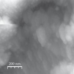
FIGURE 5.1 AFM characteristics of La2O3/HfO2 thin film MOS capacitors.
The x-ray diffraction (XRD) studies that are used to examine the structural properties of the deposited gate stack are carried out using the Rigaku, Rotaflex rotating anode XRD instrument. Figure 5.2 shows the XRD spectra of the La2O3/HfO2 gate stacks deposited by DPF. The peaks marked with #, *, and □ correspond to HfO2, La2HfO7, and La2O3. The presence of La2HfO7 peaks confirms the incorporation of lanthanum oxide in the hafnium oxide-based gate dielectric fabricated over the silicon wafer.
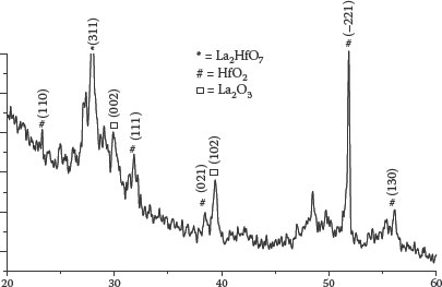
FIGURE 5.2 XRD spectra of LaO/HfO gate stacks deposited by DPF.
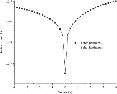
FIGURE 5.3 Current–voltage characteristics of pure La2O3/HfO2 gate dielectric stacks deposited using the DPF system under optimized conditions.
The preliminary results of capacitance versus voltage and current versus voltage characteristics are measured using an Agilent (HP) mode 4284A LCR meter and a semiconductor characterization system KEITHLEY 4200-SCS, respectively. The variation of gate current with gate voltage is plotted in Figure 5.3. The accumulation, depletion, and inversion can be clearly seen and the leakage current can be determined from the gate current versus the gate voltage graph. The variation of capacitance with gate voltage is plotted in Figure 5.4. The capacitance is measured for two DPF shots when one shot is of hafnium and the other is of lanthanum giving rise to the lanthanum-incorporated hafnium-based gate dielectric. The other important parameters such as the dielectric constant, electrical thickness, oxide capacitance, flat-band voltage, and the threshold voltage are determined and tabulated from the measurements performed at 1 MHz for the lanthanum-incorporated hafnium-based gate dielectric stacks MOS (metal–oxide–semiconductor) device deposited using two DPF shots.
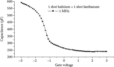
FIGURE 5.4 Capacitance–voltage characteristics of pure La2O3/HfO2 gate dielectric stacks deposited using the DPF system under optimized conditions.
TABLE 5.1
Electrical Parameters of MOS Devices at 1 MHz
Electrical Parameters |
|
Dielectric constant (ε) |
26 |
Oxide capacitance (Cox (pF)) |
590 |
Oxide thickness (Tox (nm)) |
32 |
Flat-band capacitance (CFB (pF)) |
385 |
Flat-band voltage (VFB (V)) |
−1.28 |
Threshold voltage (VTH (V)) |
−0.46 |
The dielectric constant value was determined to be 26, the oxide thickness value around 32 nm, the oxide capacitance around 590 pF, and the flat-band capacitance around 385 pF determined by measurements from a 1 MHz capacitive voltage curve. The flat-band voltage was determined to be −1.28 V, while the threshold voltage was determined to be −0.46 V for 1 MHz with a diameter of a dot around 200 μm as tabulated in Table 5.1.
Preliminary results show a successful deposition of gate dielectric stacks of La2O3/HfO2 using only two DPF shots. The AFM image shows the formation of nanostructures of La2O3/HfO2 gate stacks. The RMS roughness and average roughness of the dielectric film prepared was of the order of a few nanometers. The electrical results of the La2O3/HfO2 gate stacks deposited using two DPF shots showed improved values of capacitance with lanthanum incorporation. The other important electrical parameters such as leakage current, oxide charges/capacitance, threshold voltage, and flat-band voltage with the incorporation of lanthanum in hafnium were successfully determined. We extend our study to find the relationship between the electrical and morphological properties of La2O3/HfO2 gate dielectric stacks as an MOS structure using the DPF deposition technique. The use of a DPF machine with less processing steps for the deposition of gate dielectric stacks and avoiding the post deposition annealing steps has been well established.
The authors would like to thank Professor M. P. Srivastava, Physics Department, Delhi University, for providing useful experimental support to deposit La2O3/HfO2 gate dielectric stacks using two shots of the DPF device on silicon substrate. The authors also wish to thank Professor V. Ramgopal Rao, Electrical Engineering Department, Indian Institute of Technology, Mumbai, India, for his useful comments, suggestions, and experimental support to carry out electrical characterization under the INUP project titled “NANO SCALE MOSFETs—Scalability Issues and Possible Solutions” at IIT, Mumbai.
1. H. Wong and H. Iwai, On the scaling issues and high-κ replacement of ultrathin gate dielectrics for nanoscale MOS transistors, Microelectron. Eng. 83, 1867, 2006.
2. H. Wong and H. Iwai, The road to miniaturization, Phys. World, 18, 40, 2005.
3. A. Srivastava, R. K. Nahar, and C. K. Sarkar, Study of the effect of thermal annealing on high k hafnium oxide thin film based MOS and MIM capacitor, Journal of Materials Science: Materials in Electronics (Springer), 22, 882, 2010.
4. H. Fujisawa, A. Srivastava, K. Kakushima, P. Ahmed, K. Tsutsui, N. Sugii, T. Hattori, C. K. Sarkar, and H. Iwai, Electrical characterization of W/HfO2 MOSFETs with La2O3 incorporation, ECS Trans., 18(1), 39, 2009.
5. A. Srivastava, R. K. Nahar, C. K. Sarkar, and Y. Malhotra, Study of hafnium oxide thin film deposited using dense plasma focus machine as a gate dielectric for a MOS device, Microelectron. Reliab., 51(4), 751, 2011.
6. D. Zade, S. Sato, K. Kakushima, A. Srivastava,, P. Ahmet, K. Tsutsui, A. Nishiyama et al., Effects of La2O3 incorporation in HfO2 gated nMOSFETs on low-frequency noise, Microelectron. Reliab., 51(4), 746. 2011.
7. R. S. Rawat, M. P. Srivastava, S. Tandon, and A. Mansingh, Crystallization of an amorphous lead zirconate titanate thin film with a dense-plasma-focus device, Phys. Rev. B, 47, 4858, 1993.
8. R. Sagar and M. P. Srivastava, Amorphization of thin flim of Cds due to ion irradiation by dense plasma focus, Phys. Lett. A, 183, 209, 1996.
9. P. Agarwala, S. Annapoorni, M. P. Srivastava, R. S. Rawat, and P. Chauhan, Magnetite phase due to energetic argon ion irradiation from dense plasma focus on hematite thin film, Phys. Lett. A, 231, 434, 1997.
10. P. Agarwal, M. P. Srivastava, P. N. Dheer, V. P. N. Padmabhan, and A. K. Gupta, Enhancement in Tc of superconducting BPSCCO thick films due to irradiation of energetic argon ions of dense plasma focus, Physica C, 313, 87, 1999.