
CONTENTS
6.3 Effects of Threshold Voltage Variations
6.4 Classical, Reverse, and Optimal Transistor Sizing
Addition is a common arithmetic operation in a wide variety of digital applications. Full adder (FA) cells are used in many arithmetic operations and are crucial in both central and floating-point units. They are also used extensively for cache as well as for memory address calculations. The soaring demand for mobile electronic devices such as portable computers, smart phones, and tablets necessitates power-efficient very-large-scale integration (VLSI) circuits. As FA cells are on the critical path, they determine the system’s overall performance. That is why designing faster and low-power FAs was the main driving force behind many of the reported results [1, 2, 3 and 4].
For several decades, increasing the performance by reducing the propagation delay was the key design objective of the VLSI community. During that time, the FA’s performance and power consumption have also improved significantly due to the relentless scaling of CMOS (complementary metal–oxide–semiconductor) devices. CMOS scaling was always used to implement faster, smaller, and cheaper integrated circuits, which were optimized for minimizing delay. However, with the massive scaling of the CMOS devices, both leakage and dynamic currents have increased exponentially. Simultaneously, with the constant increase in demand for battery-operated mobile devices (especially during the last decade), energy efficiency has become the most stringent design objective, replacing propagation delay as the main design objective.
Unfortunately, the continuous scaling of CMOS technology has also brought several new challenges. With the transistor channel length closing in on 10 nm, the manufacturers run into a number of fundamental limitations. This massive scaling of the CMOS transistors is introducing large parameter fluctuations, including the threshold voltage (VTH) variations [5, 6 and7]. This has led to a constant reduction in the available reliability margins. However, most of the FA designs which have been proposed and analyzed assumed that the basic fabric of gates/transistors is reliable enough. That is why reliability was not considered as an optimization criterion. It is only very recently that the reliability of FAs has started to be thoroughly investigated [8, 10, 11 and 12]. Such papers have tried to evaluate and compare the reliability of the existing FAs, but have neglected power and delay. In Refs. [13,14], we have used a reverse sizing scheme (proposed in Ref. [15]) to simultaneously improve on both the reliability and the power efficiency of two FAs. The simulation results have shown that using the reverse sizing scheme allows for significantly improving the reliability and power efficiency at the expense of a slight increase in propagation delay.
This chapter presents yet another technique for sizing the transistors for increasing the reliability (measured here in terms of static noise margin, SNM) of FAs of different styles of design, specifically targeting advanced CMOS processes, that is, below 32 nm. The proposed sizing method takes advantage of the short channel effects (which become significant below 32 nm) by using them favorably to simultaneously increase reliability and reduce power. This chapter is organized as follows. Section 6.2 provides a brief review of low-power FAs. The effect of the transistor sizing on VTH variations is presented in Section 6.3. The classical, reverse, and optimal sizing methods are detailed in Section 6.4, followed by simulation results and analyses in Section 6.5, and the concluding remarks in Section 6.6.
Many low-power FA designs based on pass-transistor logic have been proposed [16, 17, 18 and 19]. In general, the pass-transistor FAs have fewer gates/transistors and achieve lower power consumption [20]. However, they do suffer from degraded signal levels due to VTH loss and charge sharing. One of the early low-power FA designs is the SERF (Static Energy Recovery Full adder) [16], which has two XNOR gates and one MUX (multiplexer). These three gates are implemented using 10 pass transistors.
A systematic approach for constructing 10-transistors FAs was proposed in Ref. [17]. This paper has detailed 41 different FAs based on XOR–XNOR gates. An in depth analysis has shown that three of the 41 proposed FAs consume less power than the SERF. Another FA design consists of six MUXs, each implemented by two pass transistors, for a total of 12 transistors [18]. An alternate FA design is the Complementary and Level Restoring Carry Logic (CLRCL) [19]. This FA consists of one XOR and one MUX. Both functions were implemented using pass-transistor logic. Although the CLRCL seems similar to the FAs described previously, it has the clear advantage of having only one VTH loss when compared to the other FAs which exhibit double VTH losses.
The CLRCL avoids multiple VTH losses by restoring the degraded output at each stage using CMOS inverters. The single VTH loss of the CLRCL FA design should enable it to function at lower supply voltages. Simulation results have shown that the CLRCL FA has the lowest energy consumption and lowest delay compared to the other adders in 35 nm technology [19]. Considering these advantages, we have decided to select this FA design and enhance it by replacing the pass transistors with transmission gates (TGs). These minimize signal degradation by limiting it only to charge sharing. The schematic representation of the CLRCL FA with TGs (TG FA) is shown in Figure 6.1. It should be mentioned that two inverters had to be added to the circuit presented in Ref. [19] for driving the TGs. One inverter generates the complementary input carry (Cin′), while the second one restores the voltage level of the Sum output.
6.3 EFFECTS OF THRESHOLD VOLTAGE VARIATIONS
One of the fundamental limitations of the bulk MOSFETs is their accuracy in reproducing VTH over the transistors inside a chip (intradie variations). This problem arises from the random fluctuations of both the number of dopants and of their physical locations. Previous simulations [21] have suggested that VTH variations could be approximated by a Gaussian distribution with standard deviation:
(6.1) |
where tox is the oxide thickness, NA is the channel doping, while Leff and Weff are the channel effective length and width, respectively.
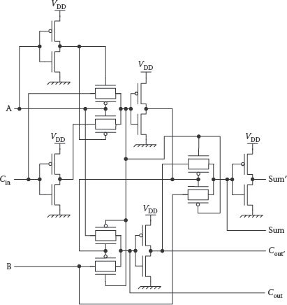
FIGURE 6.1 Schematic representation of the CLRCL FA modified by replacing the pass transistors with transmission gates (TG FA).
From Equation 6.1, it is clear that σ is inversely proportional to Weff and Leff. It follows that increasing size (Weff × Leff) will reduce σ, and should improve the transistor’s reliability. In Ref. [22], we have used σ to estimate the switching probability of failure of both nMOS and pMOS transistors. The simulation results have clearly shown that the probability of failure of the CMOS transistors depends on not only the transistor type (i.e., nMOS or pMOS) but also on the logic applied at the gate terminal (i.e., HI or LO), as well as on the variations of these voltages (which can be related to the static and dynamic noise margins of the gates). It was also shown that the switching probability of failure of a pMOS transistor is better than that of an equally sized nMOS one. The main conclusion which has emerged was that, in order to improve the reliability of CMOS gates, the reliability of the nMOS transistors has to also be improved, ideally matching the reliability of the pMOS transistors.
6.4 CLASSICAL, REVERSE, AND OPTIMAL TRANSISTOR SIZING
For classical CMOS transistors, the drive current when a transistor is “ON” is
(6.2) |
where μ* is the carrier effective mobility. As mentioned before, maximizing the performance has for many years been the fundamental objective of VLSI designers. Therefore, they routinely adjusted the sizing of the nMOS and the pMOS transistors in order to maintain the same ION current when either the pull-up (Iup) or the pull-down (Idown) stacks are switched “ON.” The aim of transistor sizing is to balance the rise and fall times. To maximize the performance while balancing the Iup and Idown currents, VLSI designers were setting the length of the nMOS and pMOS transistors to the technological minimum (LnMOS = LpMOS = min). This minimizes both the resistances and the gate’s capacitances. Afterward, the width of the nMOS was set to WnMOS = 2 × LnMOS. Finally, WpMOS was adjusted (increased) based on the gate topology such that Iup = Idown. This was required due to the difference in mobility between the holes (in case of pMOS) and the electrons (in case of nMOS).
Increasing WpMOS to balance the rise and fall times does improve the reliability of the pMOS transistors (as increasing WpMOS increases the area WpMOS × LpMOS, reducing σpMOS). However, as mentioned in Section 6.3, this does not affect the reliability of the CMOS gate because the pMOS transistors are already more reliable than the nMOS ones. Therefore, when relying on the classical sizing method, improving the nMOS’s reliability by increasing WnMOS can be done only by making WpMOS even larger. To overcome this constraint of the classical sizing, in Ref. [15], we have proposed a reverse sizing scheme. The aim of the reverse sizing scheme was to improve the reliability of the nMOS transistors by making their areas (WnMOS × LnMOS) relatively larger than the area of the pMOS transistors (WpMOS × LpMOS), while also reducing the dynamic power dissipation (as limiting ION). The reverse sizing scheme relies on the fact that changing the transistor’s W and L dimensions affects both its reliability (see Equation 6.1) and the ION current (see Equation 6.2). The reverse sizing method starts by reducing WnMOS and WpMOS to the minimum technological limit (WnMOS = WpMOS = min), which implicitly limits ION, and setting LpMOS = 2 × WpMOS. Afterward, LnMOS is increased to compensate for the difference in mobility (between electrons and holes). This is exactly the opposite of classical sizing, which keeps LnMOS and LpMOS to the technological minimum and increases WpMOS to compensate for the slower mobility of the holes.
It is worth mentioning that balancing the rise and fall times by selecting the proper transistor sizing depends on the transistor type, and on how the transistors are connected together. Transistors connected in series should be sized differently than the transistors connected in parallel or individual transistors.
The dynamic power dissipation is calculated as
(6.3) |
where a is the fraction of clock cycles in which the output transitions, C is the load capacitance, f is the switching frequency, and VDD is the supply voltage. Obviously, the simplest and most effective way to reduce power dissipation is to reduce VDD. Ultra low-power FA designs operating in sub-VTH have been proposed [2,4]. However, operating in sub-VTH raises two major concerns. The first one is that reducing VDD reduces ION, which in turn degrades the performance. The second one is that reducing VDD negatively affects the reliability [23, 24 and 25] as the effects of variations (not only VTH variations) become more pronounced.
To overcome the above constraint, an optimal sizing method is proposed here. Its aim is not only to balance the rise and fall times but also to maximize the allowed static noise margins (SNMs). Maximizing the allowed SNMs (as is commonly done for RAM cells) will push the limits where the circuit will still operate correctly, even if VDD is reduced and the variations are high. This should allow reducing VDD and the associated dynamic power dissipation. Instead of keeping one of the transistor dimensions to the technological minimum and changing the other dimension to balance the rise and fall time, the optimal sizing method works by allowing all the widths and lengths of the transistor’s channels to be adjusted simultaneously. For maximizing the SNMs, the optimal sizing method starts by taking advantage of the short channel effects and adjusts the lengths of the CMOS transistors such as VTH_nMOS = VTH_nMOS = VDD/2. Only afterward, the balancing of the rise and fall times is done by adjusting the widths of the transistors (for classical CMOS sizing).
For a specific channel length, VTH can be calculated as
(6.4) |
where VTH0 is the threshold voltage of a long channel device (10 μm) at Vbs = 0, ETA0 and ETAB are, respectively, the drain-induced barrier lowering (DIBL) coefficient in the sub-threshold region and the body-bias coefficient for the sub-threshold DIBL effect, DSUB is the coefficient exponent in the sub-threshold region, Leff is the effective channel length, Vbs_eff is the effective substrate bias voltage, Vds is the drain-to-source voltage, and lt is the characteristic length which depends on the depletion width Xdep, the oxide thickness tox, and the gate dielectric constant (see Ref. [26]).
It is clear from Equation 6.4 that VTH can easily be adjusted by slightly modifying the channel length. We have used the BSIM4v4.7 level 54 [26] for finding the optimum transistor length (Lopt) for both the nMOS and the pMOS transistors such that VTH_nMOS = VTH_pMOS = VDD/2. Afterward, we have used the classical sizing approach, that is, we set the width of the nMOS transistor to WnMOS = 2 × L min (the minimum technological size), and the width of the pMOS channel is adjusted such that the voltage transfer curve (VTC) is symmetric (a sizing which also balances the rise and fall times).
Simulations were performed to study the effect of using the optimal sizing method on the performance, the power consumption, and the reliability of two FA cells: the standard mirrored 28T FA (Figure 6.2) and the TG FA (Figure 6.1). All the simulations were done using NGSpice (ver. 24) with 22 nm Predictive Technology Model v2.1 (metal gate, high-k, and strained-Si) [27,28]. Power and delay for the FAs have been measured using the test setup circuit shown in Figure 6.3.
To calculate the SNMs, the results from NGSpice were inputted into a MATLAB script which plots the voltage transfer characteristics (VTCs) and calculates VIL, VIH, VOL, VOH, and SNM. The MATLAB script is used to automatically locate the inflection points (slope = −1) of the VTCs. The script calculates d(Vout)/d(Vin) and identifies the minimum and maximum points, which are the two points that correspond to the (VIL–VIH) and (VOL–VOH) of the VTC. The SNM is then easily calculated as min((VIL–VOL), (VOH–VIH)).
It is important to mention that, in case of multi-input–multi-output circuits such as the FA, the shapes of the VTCs (and their associated SNMs) depend upon the applied input vectors. The VTCs for the TG FA (because its SNMs are better than 28T FA) and the worst-case SNMs are shown in Figure 6.4.
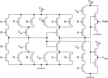
FIGURE 6.2 Schematic of the classical (standard) mirrored FA (28T FA).
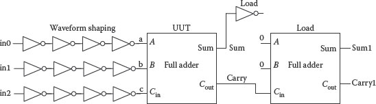
FIGURE 6.3 The test circuit used for measuring the power consumption and the delay of an FA.
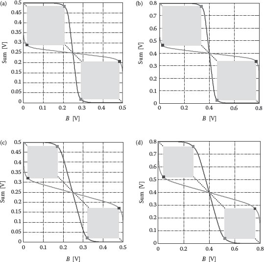
FIGURE 6.4 (a) VTC for optimally sized TG FA for input B and output Sum (when input A = 0; input Cin = 1; and VDD = 0.5 V). (b) VTC for optimally sized TG FA for input B and output Sum (when input A = 0; input Cin = 1; and VDD = 0.8 V). (c) VTC for classically sized TG FA for input B and output Sum (when input A = 1; input Cin = 0; and VDD = 0.5 V). (d) VTC for classically sized TG FA for input B and output Sum (when input A = 1; input Cin = 0; and VDD = 0.8 V).
The simulation results show that, for the 22 nm PTM HP technology, the Lopt for the pMOS nodes (Lopt_pMOS) is 29.4 nm, and for the nMOS nodes (Lopt_nMOS) it is 24.9 nm. This means that increasing the length of the nMOS channel by only 2.9 nm (13.2%) and the pMOS channel by 7.4 nm (35.9%) will improve the noise margin by setting VTH_nMOS and VTH_pMOS to VDD/2. After resolving the optimal channel length for nMOS and pMOS nodes, WnMOS is set to 44 nm and WpMOS is adjusted such that the VTCs are as balanced as possible (equivalently, the rise and fall times are balanced). Table 6.1 shows the classical and the optimal sizing for the 28T and TG-FAs.
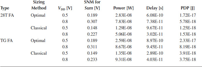
Table 6.2 shows the SNM, power, delay, and power-delay product (PDP) for the 28T FA and TG FA in case of a nominal (VDD = 0.8 V) as well as a lower supply voltage (VDD = 0.5 V). The power and delays have been measured with inputs of 50% duty cycles at a frequency of 100 MHz.
Table 6.2 shows that, in the case of nominal VDD (0.8V), using the optimal sizing method improves the SNMs of the 28T FA and the TG FA by 35% and 33%, respectively, compared to the classical sizing method. The optimal sizing method maintains its efficiency even at lower voltages. Using the optimal sizing method at VDD = 0.5V improves the SNMs of the 28T FA by 28% and of the TG FA by 27%.
A comparison between the classical and optimal-sized FAs at the same supply voltage shows that the optimally sized ones consume more power than the classical counterparts. However, such a comparison is misleading as, due to the significant improvement in SNMs, the supply voltage in case of the optimal FAs can be reduced while still achieving the same reliability as the classical designs at nominal VDD. The optimal sized FAs consume less than the classical sized FAs at the same SNM (reliability). Table 6.2 shows that using the optimal sizing method at VDD = 0.5 V will reduce the power consumption of the 28T FA by 79%, while increasing the delay by about 8× and the PDP by 3×. In the case of TG FA, using the optimal sizing method at VDD = 0.5 V reduces the power consumption by 3.34×, while increasing both the delay by 9.5× and PDP by 2.8×.
TABLE 6.1
Classical and Optimal Transistor Dimensions (nm) for 28T and TG FAs
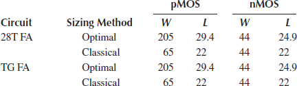
TABLE 6.2
Comparison of 28T and TG FAs under Different Conditions
A method for increasing the SNM (which is linked to reliability) of digital circuits has been introduced in this chapter. The method has been evaluated for two different FAs, the classical CMOS mirrored FA (28T FA) and the one using TGs (TG FA) when implemented in the 22 nm PTM HP. The method significantly enhances the SNMs at both the nominal as well as lower supply voltages. Additionally, the power is also reduced while the delay is increased when moving to larger channel lengths.
1. M. Alioto and G. Palumbo, High-speed/low-power mixed full adder chains: Analysis and comparison versus technology, Proc. ISCAS, New Orleans, LA, USA, May 2007, pp. 2998–3001.
2. S. Aunet, B. Oelmann, T. S. Lande, and Y. Berg, Multifunction subthreshold gate used for a low power full adder, Proc. NorChip, Oslo, Norway, Nov. 2004, pp. 44–47.
3. S. Goel, A. Kumar, and M. A. Bayoumi, Design of robust, energy-efficient full adders for deep-submi-crometer design using hybrid-CMOS logic style, IEEE Trans. VLSI Syst., 14, Dec. 2006, 1309–1321.
4. K. Granhaug and S. Aunet, Six subthreshold full adder cells characterized in 90 nm CMOS technology, Proc. DDECS, Prague, Czech Republic, Apr. 2006, pp. 25–30.
5. SIA, International Technology Roadmap for Semiconductors (ITRS), 2011 [Online]. Available at: http://public.itrs.net
6. H. Iwai, Roadmap for 22 nm and beyond (invited), Microelectr. Eng., 86, Jul.-Sep. 2009, 1520–1528.
7. C. Millar, D. Reid, G. Roy, S. Roy, and A. Asenov, Accurate statistical description of random dopantinduced threshold voltage variability, IEEE Electr. Dev. Lett., 29, Aug. 2008, 946–948.
8. S. Purohit, M. Margala, M. Lanuzza, and P. Corsonello, New performance/power/area efficient, reliable full adder design, Proc. GLSVLSI, Boston, MA, USA, May 2009, pp. 493–498.
9. T.J. Dysart and P. M. Kogge, Analyzing the inherent reliability of moderately sized magnetic and electrostatic QCA circuits via probabilistic transfer matrices, IEEE Trans. VLSI Syst., 17, Apr. 2009, 507–516.
10. H.B. Marr, J. George, D. V. Anderson, and P. Hasler, Increased energy efficiency and reliability of ultra-low power arithmetic, Proc. MWSCAS, Knoxville, TN, USA, Aug. 2008, pp. 366–369.
11. W. Ibrahim, V. Beiu, and M. H. Sulieman, On the reliability of majority gates full adders, IEEE Trans. Nanotech., 7, Jan. 2008, 56–67.
12. W. Ibrahim and V. Beiu, Threshold voltage variations make full adders reliabilities similar, IEEE Trans. Nanotech., 9, Nov. 2010, 664–667.
13. M.H. Sulieman and W. Ibrahim, Design of low-power and reliable nano adders, Proc. IEEE-NANO, Portland, USA, Aug. 2011, pp. 441–444.
14. W. Ibrahim, A. Beg and V. Beiu, Highly reliable and low-power full adder cell, Proc. IEEE-NANO, Portland, USA, Aug. 2011, pp. 500–503.
15. M.H. Sulieman, V. Beiu, and W. Ibrahim, Low-power and highly reliable logic gates: Transistor-level optimizations, Proc. IEEE-NANO, Seoul, Korea, Aug. 2010, pp. 254–257.
16. R. Shalem, E. John, and L. K. John, A novel low-power energy recovery full adder cell, Proc. GLSVLSI, Ann Arbor, USA, March 1999, pp. 380–383.
17. H. Bui, Y. Wang, and Y. Jiang, Design and analysis of low-power 10-transistor full adders using novel XOR-XNOR gates, IEEE Trans. Circuits Systems—II, 49, Jan. 2002, 25–30.
18. Y. Jiang, A. Alsheridah, Y. Wang, E. Shah, and J. Chung, A novel multiplexer-based low power full adder, IEEE Trans. Circuits Systems—II, 51, Jul. 2004, 45–48.
19. J.F. Lin, M. H. Sheu, and C. C. Ho, A novel high-speed and energy efficient 10-transistor full adder design, IEEE Trans. Circuits Systems—II, 54, May 2007, 1050–1059.
20. R. Zimmermann and W. Fichtner, Low-power logic styles: CMOS versus pass-transistor logic, IEEE J. Solid-State Circ., 32, Jul. 1997, 1079–1090.
21. A. Asenov, A. R. Brown, J. H. Davies, S. Kaya, and G. Slavcheva, Simulation of intrinsic parameter fluctuations in decananometer and nanometer-scale MOSFETs, IEEE Trans. Electr. Dev., 50, Sep. 2003, 1837–1852.
22. W. Ibrahim and V. Beiu, Using Bayesian networks to accurately calculate the reliability of complementary metal oxide semiconductor gates, IEEE Trans. Reliab., 40, Jul. 2011, 538–549.
23. D. Bol, Robust and energy-efficient ultra-low-voltage circuit design under timing constraints in 65/45 nm CMOS, J. Low Power Electr. Appl., 1, Jan. 2011, 1–19.
24. D. Bol, R. Ambroise, D. Flandre, and J.-D. Legat, Interests and limitations of technology scaling for subthreshold logic, IEEE Trans. VLSI Syst., 17, Oct. 2009, 1508–1519.
25. M. Alioto, Understanding DC behavior of subthreshold CMOS logic through closed-form analysis, IEEE Trans. Circ. & Syst. I, 57, Jul. 2010, 1597–1607.
26. BSIM4v4.7 MOSFET Model, User’s Manual, Apr. 2011, Available at: http://www-device.eecs.berkeley.edu/bsim/Files/BSIM4/BSIM470/BSIM470_Manual.pdf
27. W. Zhao and Y. Cao, New generation of predictive technology model for sub-45 nm early design exploration, IEEE Trans. Electr. Dev., 53, Nov. 2006, 2816–2823.
28. Predictive Technology Model [Online]. Available at: http://ptm.asu.edu