
Package-Compatible High-Density Nano-Scale Capacitors with Conformal Nano-Dielectrics |
CONTENTS
7.2 Etched-Foil Nanocapacitors
Passive components support key electrical functions in any electronic system. They constitute ~80% of all components [1] and take up to ~50% of the printed wiring board area [2]. They, therefore, substantially influence the size, cost, and performance of the electronic system as a whole. Capacitors (C) are the most challenging among all the passives (R, L, and C). They perform a multitude of important functions such as decoupling, noise suppression, power storage conditioning and modulation, sensing, and signal processing. The never-ending demand for the high-performance, portable electronics has propelled the need for miniaturization of electronic components, including the capacitors. This demand for miniaturization entails the fabrication of thin power modules that are less than 200 μm in thickness to be embedded into 3D silicon and organic packages [3]. Additionally, these packages need to be reliably and safely operated over a broad temperature range [4]. So far, these passive components, especially the capacitors, have been major impediments on the road to system miniaturization and thickness reduction. Although the demand for high-density capacitors in integrated thin power modules has been increasing, the volumetric density of the available discrete capacitors has only gone through incremental changes over the past few decades. This is because of several fundamental limitations with existing capacitor technologies. Today’s high-density capacitors face the imminent demand of ultrahigh volumetric densities, ultralow leakage currents, high-frequency operation, and faster charge–discharge speeds. The current capacitor technologies are stretching their limits to explore novel materials, processes, and integration methods to meet the demands, but suffer from several fundamental limitations. A new class of nanocapacitor technologies is needed to address these limitations, which is the main focus of this chapter.
Starting from the origins of the capacitor that can be traced back to the invention of the Leyden jar, a ceramic capacitor [5], the capacitor technology has taken a leap through its 250 years of technical evolution. The capacitor development process has been evolutionary rather than revolutionary. Early development was primarily driven by the need for banks of low-cost energy storage capacitors used in large-pulse power systems. The production of aluminum electrolytic capacitors in 1936 was a stepping stone toward the production of commercial capacitors and was widely used during the Second World War [6]. The discovery of barium titanate (BT) (with a relative permittivity of 1000) in 1941 [7] and its family of materials, thereafter, led to its use as a passive electronic component in a host of defense equipment. The use of fabrication technologies such as tape casting and the ceramic electrode cofiring process during the 1970s and 1980s led to the development of the multilayer ceramic capacitor (MLCC). The MLCC-based capacitors have demonstrated the potential to achieve capacitance densities in the range of 100 μF/cm2. Dielectrics such as BT used in MLCCs have high dielectric constants. As of 2010, the global annual BT-based MLCC stands at 1 trillion units. However, they are incompatible with silicon because of their high-temperature processing requirements. Therefore, they cannot be integrated into silicon packages as thin films. The state-of-the-art tantalum-based capacitor technology with high volumetric densities serves as an alternative route to the above approach. There are also several issues, though, with the integration of existing tantalum-based capacitors into the silicon package. Tantalum processing with existing microparticles requires high-temperature processing in the range of more than 1500°C [8]. Moreover, the volumetric density of the system is further reduced in the final system when the packaging volume is taken into account. Trench capacitors address the limitations of achieving high capacitance density using thin films on the walls of the trench in silicon. However, the silicon trench capacitors have not exceeded capacitance densities of more than 40–50 μF/cm2 and yet suffer from the need for high-cost tools [9]. In view of the above limitations, researchers around the globe are working on novel capacitor technologies to pursue high capacitance densities (>100 μF/cm2) in thin-film high-density capacitors. A simple 2D graph in Figure 7.1 shows the effective surface area enhancement and the corresponding capacitance densities of the current and emerging technologies.
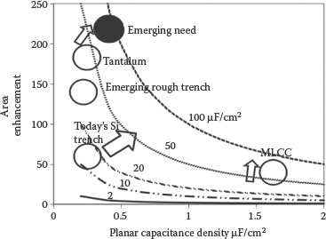
FIGURE 7.1 Volumetric densities of various state-of-the-art and emerging capacitor technologies.
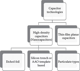
FIGURE 7.2 Classification scheme for various capacitor technologies.
The basic capacitor technology meets its target capacitance by enhancing one or more of the three fundamental parameters—electrode surface area, dielectric permittivity, and thinner dielectric. Combining the three parameters in the best way to achieve the highest capacitance density, lowest leakage currents, and highest reliability remains the ultimate goal for most of the capacitor applications. While dielectric permittivity is a material-dependent parameter, the electrode surface area and the thickness of the deposited dielectric are both process-driven. Based on these critical, process-driven parameters, the state-of-the-art capacitor technologies are broadly categorized as planar and 3D high-density capacitors (shown in Figure 7.2).
The “planar” capacitors require planar (2D) electrode surfaces, but utilize ultrathin, high-permittivity dielectrics such as barium–strontium titanates (BST), strontium titanates (ST), or BT. On the other hand, the current “three-dimensional” or high-density capacitors utilize extremely high electrode surface areas with low-to-moderate permittivity dielectrics. These include a silicon trench [10], MLCCs [11], and particulate capacitors (tantalum based) [12]. More recently, there is an increasing focus on benefiting from all the three key capacitance parameters, viz., ultrahigh surface electrode area, thin dielectrics with high permittivity in the same component. This new class of capacitors is termed “nanocapacitors” and will be the focus for this chapter. For an easier and more comprehensive understanding, the chapter will be divided into etched foil nanocapacitors, silicon trench nanocapacitors, and nanoparticulate-based capacitors.
7.2 ETCHED-FOIL NANOCAPACITORS
Adding a new dimension to the planar electrodes is the key to increase the surface area and thereby the volumetric density of the capacitors. The most commonly used method to do so is by etching deep and porous channels inside the electrode. Silicon, aluminum, and titanium are some of the electrode systems that are commonly etched using electrochemical (wet-etching) or reactive plasma (dry-etching) processes [13, 14, 15, 16 and 17] to yield high-aspect-ratio deep channels or trenches. Depositing conformal high-permittivity dielectrics over larger areas is critical to form the capacitor and usually requires vapor deposition techniques such as chemical vapor deposition (CVD) and atomic layer deposition (ALD) [18]. These deposition techniques have their set of drawbacks, which includes high cost, high deposition time, and low throughput. On the other hand, methods such as thermal oxidation or nitridation limit the dielectrics to lower permittivity values. To circumvent these issues, anodizable metals, also known as valve metals, such as Al, Ta, Ti, and Nb [19], have been widely used as nanoelectrode templates for the fabrication of nanocapacitors. Here, the dielectric formation is accomplished by oxidizing the electrode surface by immersing the etched metal into an electrolyte solution and applying a voltage bias to the electrode. This method, known as anodization, is widely used in the electrolytic capacitor and tantalum industry. The consistency, conformality, and thickness uniformity of the dielectric are monitored by the time, current, voltage, and the concentration of the electrolyte. The liquid electrolyte is capable of reaching the narrowest channel in the metal, which, on contact with the metal surface, oxidizes to form a dielectric oxide on the anode. The dielectric thickness increases with the anodizing voltage at a rate of ~1–2 nm/V [20]. It is known that out of all the available dielectric materials, oxides, nitrides, and oxynitrides have the highest breakdown voltages. This implies that these dielectric films can be easily thinned down to a few 10 s of nanometers without compromising on their reliability. The oxide layer formed during anodization shows a voltage-dependent resistance that causes the current to increase more steeply as the voltage increases during anodization. The rated anodizing, and the operating voltages are carefully designed to produce safe and reliable capacitors.
The counter electrode used for these capacitors is usually a liquid electrolyte. Aluminum electrolytic capacitors are also designated as “wet” or “nonsolid” capacitors due to the use of liquid electrolyte as the cathode. The liquid has the advantage of filling the deep-etch structures or channels, thus optimally fitting into the anode structure and accessing the high-surface-area electrode. A conventional aluminum electrolytic capacitor thus consists of a wound capacitor element that is impregnated with a liquid electrolyte, connected to terminals, and sealed in a can. The element is composed of an anode foil, paper separators saturated with an electrolyte, and a cathode foil. These capacitors routinely offer capacitance values from 0.1 μF to 3 F and voltage ratings from 5 to 700 V.
They are polar devices, having distinct positive and negative terminals, and are offered in several design configurations. Though these conventional liquid aluminum electrolytic capacitors provide high capacitance densities required for various applications such as decoupling, power, noise suppression, and so on, there are several limitations associated with these electrolytic capacitors. Some of the major disadvantages are the high impedance and thermal instability, and liquid electrolyte leakage, owing to the use of a low-conductive (10−2–10−3 S/cm) and thermally unstable ionic liquid electrolyte.
To cope with these limitations, solid aluminum capacitors using solid counter electrodes have been developed. The most prominent solid counter electrodes are broadly classified as organic and inorganic counter electrodes based on their chemical properties. Conducting polymers such as polyethylenedioxythiophene (PEDT), poly-3-hexylthiophene (P3HT), polyethylene oxide (PEO), polypyrrol, and complexes such as tetracyanoquinodimethane (TCNQ) are organic counter electrodes, while pyrolytic manganese dioxide and ruthenium oxide are categorized as inorganic counter electrodes. These solid counter electrode based capacitors have several advantages over the traditional liquid electrolytic capacitors. For example, PEDT polymer-based capacitors have lower equivalent series resistance (ESR) than the liquid electrolytic capacitors because of the higher conductivity of PEDT [21]. This permits a single polymer-type capacitor to replace several liquid aluminum electrolytic-type capacitors, resulting in a reduced total number of components on the board and more available real estate. Moreover, since the polymer is a solid, it also gives longer life, not following the classic Arrhenius formula. Instead of doubling life with every 10°C drop in temperature, the lifetime will be 10 times longer for every 20°C decrease in temperature. Another key advantage of the solid electrolyte over the liquid ones is their capability to heal the defects or pinholes in the dielectrics. Manganese dioxide (MnO2) and PEDT are widely used in tantalum particulate capacitors as self-healable counter electrodes. The self-healable mechanism in Al-electrolytic capacitors with MnO2 as the counter electrode is shown in Figure 7.3.
This self-healing process is an important factor in the steady-state reliability characteristics of tantalum capacitors, which are referenced as having “no wear-out mechanism.” In MnO2-based self-healable reactions, the conductive MnO2 electrode is locally converted to highly resistive Mn2O3, as shown in Reaction 7.1:
(7.1) |
Aluminum oxide (Al2O3) has pinholes or defects or regions thinner than the surrounding dielectric. A large proportion of the capacitor current (charging, leakage) flows through the leaky site causing excessive localized heating. As the temperature at the defect site rises, Reaction 7.1 takes place, converting the conductive manganese dioxide (MnO2), which has a resistivity of between 1 and 10 ohm/cm2, to a less conductive form (Mn2O3) having a resistivity between 106 and 107 ohm/cm2. Thus, the conduction site is effectively “plugged” or “capped,” thereby decreasing the leakage current.
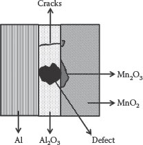
FIGURE 7.3 Self-healing mechanism of MnO2 in Al/Al2O3 system.
Though MnO2 has shown several benefits as a counter electrode in Al- and Ta-based capacitors, it is unsafe during high-voltage operation since it forms an ignitable redox couple with metal at higher voltages [22]. Other limitations such as high ESR due to higher resistivity have led to the use of alternative cathode materials such as conducting polymers. Among the intrinsically conducting polymers (ICPs), thiophenes are most widely used in the capacitor industry due to numerous advantages such as higher conductivity, improved safety, and self-healing. PEDT is one classic ICP with much higher conductivity than MnO2, thereby lowering the characteristic ESR in the capacitor [23]. Furthermore, it has improved safety aspects during the high-voltage operation. In addition, PEDT possesses self-healing ability, high-temperature stability, and outstanding electronic properties in the doped as well as undoped states. Even with those attractive merits, PEDT-based capacitors exhibit poorer electrical characteristics such as high leakage currents as the operating voltage of the Ta and Al electrolytic capacitors is increased [24]. The conducting polymer deposition method plays a critical role in determining the leakage properties of the fabricated capacitor. In situ deposition of conducting polymers such as PEDT has generally shown poor electrical characteristics due to the chemical interactions between the oxide dielectric and the residual oxidizers entrapped in the deep Al/Si trenches. Tantalum capacitors that use PEDT as the cathode electrode eliminate the residual oxidizers by carrying out several cycles of washing and reformation (reanodization to form the dielectric). More recently, prepolymerized PEDT polymer dispersions have also been introduced to tantalum technology, greatly improving the capacitor voltage ratings of 25 V and reliability [25].
Titanium nitride (TiN) deposited through ALD has recently gained momentum due to its high conductivity and conformality across deep trenches [26]. ALD, being self-limiting (deposition of one atomic or molecular layer in each reaction cycle) in behavior, is capable of sequentially depositing conformal thin films of materials (metals and dielectrics alike) onto substrates with complex, contoured surfaces. It has become the leading process to achieve such coatings, yielding a high degree of thickness control and conformality in the most demanding nanostructures. Banerjee et al. [27] have demonstrated metal–insulator–metal (MIM) nanocapacitor arrays with ALD inside AAO (anodized aluminum oxide) nanopores, making use of self-assembly and self-alignment. ALD titanium nitride formed the bottom as well as the top electrode, whereas ALD Al2O3 was sandwiched as the dielectric. The highly regular arrays in AAO have reported a capacitance density of 100 μF/cm2 for 10-μm-thick anodic aluminum oxide.
The Packaging Research Center at the Georgia Institute of Technology has coupled the low-cost dielectric deposition technique with top electrode ALD to show a cost-effective approach to high-density nanocapacitors that has the potential to be integrated directly into silicon or glass substrates. Commercially available etched aluminum foils, capable of introducing 50–100 times more the surface area depending upon the foil thickness and the extent of etch, were utilized as the bottom electrode. These metal foils were anodized with respective chemistries to yield highly conformal, uniformly thick dielectrics. The anodized metal foils can be subsequently integrated into organic packages by traditional processes such as lamination and etching. Etched foils with 75–105-μm thickness, having channels with an aspect ratio of above 50, were used in this study. The SEM image of the 75-μm-thick etched Al foil is shown in Figure 7.4a. ALD TiN was used as the counter electrode of the capacitor because of its ability to conformally coat the higher surface area of the anodized etched foil. An approximately 20-nm-thick blanket TiN film deposited by ALD was patterned using dry photoresist as an etch mask to isolate smaller devices. Reactive ion etcher (RIE) was used for the nitride etching process (with the following parameters: SF6—45 sccm, O2—5 sccm, RF power: 350 W). A step-by-step illustration of the procedure for the fabrication of etched-metal nanocapacitors is shown in Figure 7.4b. Such low-temperature, low-cost, high-density nanocapacitors showed capacitance densities of above 6–7 μF/cm2 at kHz frequencies, which are significantly higher than what are feasible with high-permittivity thin-film capacitors so far, demonstrated with high-temperature processes.
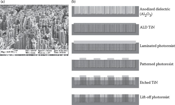
FIGURE 7.4 (a) SEM micrograph of the 75-μm-thick etched Al foil; (b) Step-by-step fabrication of the etched Al capacitor with ALD TiN as a top electrode.
Silicon trench capacitors were introduced to miniaturize the decoupling capacitors in high-performance processors. The idea of using high-value metal oxide semiconductor (MOS) capacitors made in silicon with enlarged surface using etched ridges in Si was first proposed by Rosenfeld [28] and then by Lehmann et al. who used arrays of deep trenches [29,30]. As the surface opening of the storage capacitor is scaled down, adequate capacitance is maintained by etching deeper trenches. Submicrometer opening trenches with aspect ratios of above 40 were reported by IBM in the late 1980s [31]. Equivalent capacitance densities of 10–20 μF/cm2 were reported in 1991, but with micrometer-scale dimensions leading to fF capacitors. This technology is now implemented over larger areas to yield μF capacitors with millimeter or centimeter dimensions using deep silicon trenches over a large area with high K dielectrics. The silicon trench formation processes can be classified into wet-etching and dry-etching processes, where dry etching uses inductive coupled plasma with fluorine chemistry, which then diffuses to the low-pressure etching chamber where silicon is processed. Wet etching, on the other hand, is a low-cost, fast-etching technique that is accomplished with photo electrochemical method.
The deposition of dielectrics in silicon trenches is usually achieved with reasonable conformality using CVD techniques [32]. Liquid-phase CVD and thermal oxynitridation are known to be conformal and compatible with active circuitry [33]. Therefore, these techniques are widely pursued as the oxynitride deposition route. Other alternate routes include thermal oxidation and nitridation. However, ALD [34] is usually the preferred route for uniform step coverage unlike CVD. Silicon oxide is the traditional dielectric choice because of its high breakdown voltage and compatibility with silicon. A further increase of capacitance was obtained by introducing a pure nitride dielectric, without oxide, where leakage is reduced by operation at a lower voltage (Vdd from 1.8 to 1.2 V) for dynamic random-access memory (DRAM) applications [35]. ALD is pursued as the most versatile technique to deposit high K materials with thickness uniformity, step coverage, and relatively low temperatures. Several higher-permittivity dielectrics such as Al2O3, HfO2, TiO2, and Ta2O5 have been deposited by ALD in deep trenches to enable high capacitance densities. State-of-the-art industrial trench capacitors in silicon reach capacitance densities up to 200 nF/mm2 at 11 V breakdown voltage [36]. More recently, results on multilayer MIM capacitors with ALD Al2O3 dielectric layers [37] have shown a different way to increase the capacitance density as compared to earlier works on single-layer MIM capacitors [38,39]. Kammerer et al. reported the fabrication and characterization of multiple MIM capacitors by depositing TiN/Al2O3/TiN/Al2O3/TiN stacks by ALD in deep trenches with an aspect ratio of 20, yielding a very high capacitance density of 440 nF/mm2 at a breakdown voltage (BDV) >6 V [37,40].
Even with the advances and improvements in the ALD technique, the process of metal and dielectric deposition by ALD remains challenging due to the low-throughput vacuum tools, costly precursors, packaging-incompatible infrastructure, and scaling costs. Chemical solution deposition, including sol–gel and other solution-deposition techniques, offers a low-cost route to derive inorganic thin films with much higher K than the ALD oxides. Integration of thin-film sol–gel-derived ceramic capacitors has been demonstrated in both organic packages and silicon [41,42]. GT-PRC has shown an innovative and low-cost solution-coating technology to form conformal electrodes and dielectrics in silicon trench structures to form trench capacitors. An all-solution-derived capacitor with a PZT/LNO/SiO2/Si structure was demonstrated [42]. Vacuum-infiltration was carried out to conformally coat the sol–gel precursors on the deep trenches by applying a controlled pressure gradient over the wafer that drove the solution down the trench surfaces [42]. A schematic 3D structure thus formed by the sol–gel vacuum infiltration technique is shown in Figure 7.5a. A SEM cross-section of the conformal sol–gel coating along the via wall is also shown in Figure 7.5b. Multiple coatings were applied to increase the coating thickness before thermally annealing the films in air at high temperatures (>700°C). A representative SEM image of the sol–gel-deposited (PZT/LNO/SiO2/Si) is shown in Figures 7.6a and b [42]. The thin films showed a capacitance density of 2–3 μF/cm2. In conjunction with the planar capacitors demonstrated, the feasibility of conformal solution coatings in trenches with an aspect ratio of 5–10 can potentially lead to a capacitance density of 10–30 μF/cm2, which can meet the emerging needs for thin power supply capacitors in a silicon interposer. These thin capacitor components can then be embedded in the package to enable true system integration and miniaturization.
The approach to a ultrahigh-surface-area bottom electrode is achieved by sintering valve metal particles on a metal wire. This ultrahigh surface area is capable of providing high volumetric density in capacitors. Tantalum capacitors are the most widely and commercially manufactured discrete capacitors. These are fabricated by sintering micrometer-sized tantalum powder into a pellet. The pellets are sintered with controlled open-pore volume. The particles create point contacts with each other in random fashion, leaving large gaps between most of the particles. Thus, the pressed tantalum pellet is a highly porous metal with channels or tunnels that are interconnected throughout the pellet and extends to the outside surface. Figure 7.7 shows the illustration of a tantalum capacitor. The volume enhancement for particulate electrodes is a function of the particle’s packing fraction and the particle size. Tantalum requires very high temperatures for sintering (>1400°C), thus making it incompatible for silicon or organic packages.
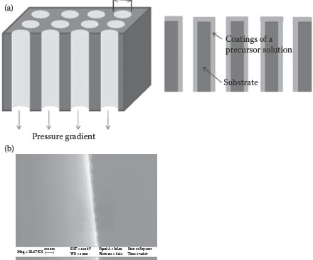
FIGURE 7.5 Schematic representation of a three-dimensional trench structure after sol–gel vacuum infiltration. Cross-section of a conformal ceramic coating along the via wall.
Tantalum capacitors employ the anodization technique for dielectric deposition. Being a valve metal, tantalum forms an insulating oxide when a potential is applied in an electrolytic bath. For the capacitor application, pressed and sintered tantalum pellets are immersed into an electrolytic solution as an anode. The liquid electrolytes seep inside the narrow tunnels of the pellet, converting the metal into the oxide, Ta2O5. The depth and consistency of the Ta2O5 layer are usually determined by the time, current, and the applied voltage during the anodization process. The thickness of the dielectric is in the range of 18 Å/V [43]. The capacitors are polar. Therefore, the dielectric is more stable when the tantalum is used as the anode. Any reverse bias can destabilize the dielectric by depleting the oxygen in the dielectric. Thus, the Ta2O5 layer is generally reformed (posthealed) before the cathode (top electrode) is deposited. This is accomplished to prevent high initial leakage that will otherwise deteriorate the dielectric until it is completely damaged in that area and lead to shorting of the capacitor as a whole. Therefore, tantalum capacitors employ self-healable materials such as manganese dioxide (MnO2) which can heal dielectric defects that can otherwise cause reliability issues. MnO2 electrodes are formed by dipping the tantalum pellet in Mn(NO3)2, followed by pyrolyzing the salt to convert into the oxide. This process is repeated to fill the tantalum pellet. Typically, this conversion process takes place at a temperature range of 200–280°C. The MnO2 now extends into the pellet and covers the outside surface of the pellet. The pellet is then dipped in a carbon solution, and subsequently in silver paints and cured. The silver paint surface is connected to a lead-frame element with a conductive epoxy and the tantalum riser wire is welded to another lead-frame element. The structure is then packaged with the lead frame extending out through the plastic. When normalized to 100-μm thickness, commercially available tantalum capacitors have shown a capacitance density of 140 μF/cm2 with a voltage rating of 6 V. For a 10 V rating, 100 μF/cm2 is available, whereas only 15 μF/cm2 is available for a voltage rating of above 20 V. Furthermore, the leakage currents are generally reported to be close to 0.1 μA/μF.
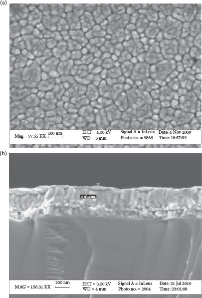
FIGURE 7.6 SEM micrographs of the PZT/LNO/SiO2/Si system: (a) top view and (b) cross-sectional view.
Besides their ultrahigh capacitance densities, tantalum capacitors have traditionally had two weaknesses—a susceptibility to ignition when they fail and higher ESR than that from other capacitor technologies. Moreover, the tantalum capacitors, owing to their high processing temperatures, remain silicon- and package-incompatible and are limited by the moderate K dielectric, Ta2O5. Though the safety and the ESR concerns are addressed by introducing conductive polymer (PEDT) as a replacement for the conventional manganese dioxide, tantalum processing temperatures and the restriction to use high K dielectrics remain a major bottleneck for tantalum capacitors.
To address the challenges posed by valve metals and to advance further in capacitance densities with integrable approaches, low-temperature sinterable metals such as copper are pursued. This also opens an avenue to deposit high K ferroelectrics as dielectrics, which is not feasible with tantalum particles. GT-PRC has shown the feasibility of high-density nanocapacitors, utilizing copper particulate electrodes, ALD alumina as a dielectric, and conducting polymer as the counter electrode [44]. These capacitors showed a capacitance density of 60 μF/cm2 using low-temperature, silicon- or package-compatible processes. The cross-section of the capacitor is illustrated in Figure 7.8. The thicker electrode capacitors showed as high as 400–500 times surface area enhancement, corresponding to a much higher capacitance density. The capacitance versus voltage plots for copper nanoparticulate capacitors based on the thickness of the electrode are shown in Figure 7.9 [44]. The capacitance density corresponds to 60 μF/cm2.
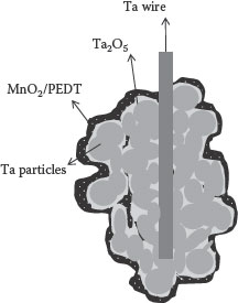
FIGURE 7.7 Cross-section of a discrete tantalum capacitor with Ta wire for interconnection.
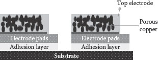
FIGURE 7.8 Integrated high-density nanocapacitor with a copper nano-electrode.
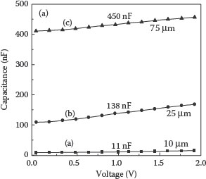
FIGURE 7.9 Capacitance vs. applied voltage curves of the copper nano-electrode capacitors. The electrode thickness is shown for each curve.
This novel particulate capacitor technology is unique compared to current technologies, such as MLCC, trench, and tantalum, in many ways: (1) There is direct deposition of particulate electrodes onto silicon as thin integrated passive device (IPD) or interposer architectures, unlike the bulky surface mount discretes (SMD). (2) It is a combination of high K films and high-surface-area electrode technologies. The highest capacitance density can thus be, obtained with leading edge particulate electrode technologies. (3) Capacitor arrays can be formed in a planar format with multiple independent terminals that are compatible with a thin silicon IC stack on the top. This unique nanoelectrode capacitor technology thus goes beyond the current technologies and has the potential of achieving higher volumetric capacitance density with superior leakage current, breakdown voltage, and ESR properties.
The need for miniaturized passive components arises from the increasing demand for lighter, higher-performance, and highly integrated ultrathin packages at reduced cost. This chapter discusses one aspect of these passive components, that is, the state-of-the-art high-density capacitor technologies, benchmarking them against their capacitance densities, silicon and package compatibility, low-cost manufacturable processes, and electrical properties such as leakage current and breakdown voltages. The demand for high capacitance densities in microscaled device dimensions has provided the motivation to develop nanocapacitors with unique electrode structures and designs, as well as superior material properties and processes. Three classes of nanocapacitors, viz., etched foils, silicon trench, and particulate types, were discussed in this chapter. A consolidated understanding of the role of high-surface-area electrodes, along with high-permittivity dielectrics in fabricating nanocapacitors with ultrahigh capacitance densities, has been provided. Novel high-surface-area nanoporous electrode technologies with a conformal dielectric for integration of high-density capacitors as thin films on silicon and glass with densities of 100 μF/cm2 using 100-μm-thick films are discussed.
1. Raj PM, Sharma H, Sethi K, Wang Y, Sundaram V, Tummala R. Thin film power components with nanoscale electrodes and conformal dielectrics. In: IEEE International Conference on Nanotechnology 2011: 106–110.
2. Tummala RR. Fundamentals of Microsystems Packaging. McGraw-Hill, New York 2001, 7:2.
3. Raj PM, Sharma H, Mishra D, Chakraborti P, Lei S, Yang I, Tummala R. Silicon- and glass-integrated thin film power components. In: CARTS International. Las Vegas 2012.
4. Brennecka GL, Ihlefeld JF, Maria JP, Tuttle BA, Clem PG. Processing technologies for high-permittivity thin films in capacitor applications. Journal of the American Ceramic Society 2010, 93(12):3935–3954.
5. Ho J, Jow TR, Boggs S. Historical introduction to capacitor technology. In IEEE: Electrical Insulation Magazine 2010, 26(1):20–25.
6. Niwa S, Taketani Y. Development of new series of aluminium solid capacitors with organic semiconductive electrolyte (OS-CON). Journal of Power Sources 1996, 60(2):165–171.
7. Mansbridge G.F. Patent 19,451. UK; 1900.
8. Balaji T, Govindaiah R, Sharma M, Purushotham Y, Kumar A, Prakash T. Sintering and electrical properties of tantalum anodes for capacitor applications. Materials Letters 2002, 56(4):560–563.
9. Hoogeland DJ, Jinesh K, Roozeboom F, Besling W, Lamy Y, Van de Sanden M, Kessels W. Plasmaassisted ALD of TiN/AlO stacks for MIMIM trench capacitor applications. ECS Transactions 2009, 25(4):389–397.
10. Katsumata R, Tsuda N, Idebuchi J, Kondo M, Aoki N, Ito S, Yahashi K, Satonaka T, Morikado M, Kito M. Fin-array-FET on bulk silicon for sub-100 nm trench capacitor DRAM. In: IEEE Symposium on VLSI Technology 2003: 61–62.
11. Pithan C, Hennings D, Waser R. Progress in the synthesis of nanocrystalline BaTiO3 powders for MLCC. International Journal of Applied Ceramic Technology 2005, 2(1):1–14.
12. Larmat F, Reynolds JR, Qiu YJ. Polypyrrole as a solid electrolyte for tantalum capacitors. Synthetic Metals 1996, 79(3):229–233.
13. Blauw M.A, van Lankvelt P, Roozeboom F, van de Sanden M, Kessels W. High-rate anisotropic silicon etching with the expanding thermal plasma technique. Electrochemical and Solid-State Letters 2007, 10(10):H309–H312.
14. Diesinger H, Bsiesy A, Herino R. Nano-structuring of silicon and porous silicon by photo-etching using near field optics. Physica Status Solidi (a) 2003, 197(2):561–565.
15. Kemell M, Ritala M, Leskelä M, Ossei-Wusu E, Carstensen J, Föll H. Si/Al2O3/ZnO: Al capacitor arrays formed in electrochemically etched porous Si by atomic layer deposition. Microelectronic Engineering 2007, 84(2):313–318.
16. Smela E, Kallenbach M, Holdenried J. Electrochemically driven polypyrrole bilayers for moving and positioning bulk micromachined silicon plates. Journal of Microelectromechanical Systems 1999, 8(4):373–383.
17. Van Den Meerakker J, Elfrink R, Weeda W, Roozeboom F. Anodic silicon etching; the formation of uniform arrays of macropores or nanowires. Physica Status Solidi (a) 2003, 197(1):57–60.
18. Elam J, Routkevitch D, Mardilovich P, George S. Conformal coating on ultrahigh-aspect-ratio nanopores of anodic alumina by atomic layer deposition. Chemistry of Materials 2003, 15(18):3507–3517.
19. Kukli K, Ritala M, Leskelä M. Development of dielectric properties of niobium oxide, tantalum oxide, and aluminum oxide based nanolayered materials. Journal of the Electrochemical Society 2001, 148:F35.
20. Velten D, Biehl V, Aubertin F, Valeske B, Possart W, Breme J. Preparation of TiO2 layers on cp-Ti and Ti6Al4V by thermal and anodic oxidation and by sol-gel coating techniques and their characterization. Journal of Biomedical Materials Research 2002, 59(1):18–28.
21. Kirchmeyer S, Reuter K. Scientific importance, properties and growing applications of poly (3,4-ethylenedioxythiophene). Journal of Materials Chemistry 2005, 15(21):2077–2088.
22. Freeman Y, Harrell W, Luzinov I, Holman B, Lessner P. Electrical characterization of tantalum capacitors with poly(3,4-ethylenedioxythiophene) counter electrodes. Journal of the Electrochemical Society 2009, 156:G65–G70.
23. Prymak JD. Replacing MnO2 with conductive polymers in Tantalum capacitors. In: CARTS. Europe 2009.
24. Alapatt G.F, Harrell WR, Freeman Y, Lessner P. Observation of the Poole-Frenkel effect in tantalum polymer capacitors. In: IEEE SoutheastCon 2010: 498–501.
25. Reed E, Haddog G. Reliability of high-voltage tantalum polymer capacitors, CARTS 2011 Proceedings, March 28–31, Jacksonville, FL, pp. 1–13.
26. Blomberg T, Wenger C, Kaynak C.B, Ruhl G, Baumann P. ALD grown NbTaOx based MIM capacitors. Microelectronic Engineering 2011, 88(8):2447–2451.
27. Banerjee P, Perez I, Henn-Lecordier L, Lee S.B, Rubloff G.W. Nanotubular metal–insulator–metal capacitor arrays for energy storage. Nature Nanotechnology 2009, 4(5):292–296.
28. Rosenfeld R, Bean K. Fabrication of topographical ridge guides on silicon for VHF operation. In: IEEE Ultrasonics Symposium 1972: 186–189.
29. Foell H, Lehmann V. Etching method for generating apertured openings or trenches in layers or substrates composed of n-doped silicon. Patent 4874484. US; 1989.
30. Lehmann V, Föll H. Formation mechanism and properties of electrochemically etched trenches in n-type silicon. Journal of the Electrochemical Society 1990, 137:653–659.
31. Rajeevakumar TV, Lii T, Weinberg ZA, Bronner GB, McFarland P, Coane P, Kwietniak K, Megdanis A, Stein K.J, Cohen S. Trench storage capacitors for high density DRAMs. Electron Devices Meeting, Technical Digest, International 1991: 835–838.
32. IslamRaja MM, Cappelli M, McVittie J, Saraswat K. A 3-dimensional model for low-pressure chem-ical-vapor-deposition step coverage in trenches and circular vias. Journal of Applied Physics 1991, 70(11):7137–7140.
33. Lin CC, Wei RC. Nitrogen-plasma treatment of carbon nanotubes and chemical liquid phase deposition of alumina for electrodes of aluminum electrolytic capacitors. Journal of the Electrochemical Society 2012, 159(5):A664–A668.
34. Lee B, Park SY, Kim HC, Cho KJ, Vogel EM, Kim MJ, Wallace RM, Kim J. Conformal Al2O3 dielectric layer deposited by atomic layer deposition for graphene-based nanoelectronics. Applied Physics Letters 2008, 92(20):203102–203103.
35. Liu C.H, Wu JM. Improvement of electrical properties and reliability of (BaSr) TiO thin films on Si substrates by NO prenitridation. Electrochemical and Solid-State Letters 2006, 9(2):G23–G26.
36. Roozeboom F, Klootwijk J, Verhoeven J, Heuvel FC, Dekkers W, Heil S, Hemmen J.L, Sanden M.C.M, Kessels W, LeCornec F. ALD options for Si-integrated ultrahigh-density decoupling capacitors in pore and trench designs. ECS Transactions 2007, 3(15):173.
37. Klootwijk J, Jinesh K, Dekkers W, Verhoeven J, Van Den Heuvel F, Kim HD, Blin D, Verheijen M, Weemaes R, Kaiser M. Ultrahigh capacitance density for multiple ALD-grown MIM capacitor stacks in 3-D silicon. IEEE Electron Device Letters 2008, 29(7):740–742.
38. Bajolet A, Giraudin J, Rossato C, Pinzelli L, Bruyère S, Crémer S, Jagueneau T, Delpech P, Montès L, Ghibaudo G. Three-dimensional 35 nF/mm2 MIM capacitors integrated in BiCMOS technology. In: IEEE Solid-State Device Research Conference 2005: 121–124.
39. Gutsche M, Seidl H, Luetzen J, Birner A, Hecht T, Jakschik S, Kerber M, Leonhardt M, Moll P, Pompl T. Capacitance enhancement techniques for sub-100 nm trench DRAMs. In: IEEE Electron Devices Meeting 2001: 18.16.11–18.16.14.
40. Matters-Kammerer MK, Jinesh KB, Rijks TGSM, Roozeboom F, Klootwijk JH. Characterization and modeling of atomic layer deposited high-density trench capacitors in silicon. IEEE Transactions On Semiconductor Manufacturing 2012, 25(2): 247–254.
41. Abothu I.R, Raj P.M, Hwang J.H, Kumar M, Iyer M, Yamamoto H, Tummala R. Processing, properties and electrical reliability of embedded ultra-thin film ceramic capacitors in organic packages. In: IEEE Electronic Components Technology Conference 2007: 1014–1018.
42. Wang Y, Xiang S, Raj P, Sharma H, Williams B, Tummala R. Solution-derived electrodes and dielectrics for low-cost and high-capacitance trench and Through-Silicon-Via (TSV) capacitors. In: IEEE Electronics component Technology Conference 2011: 1987–1991.
43. Klerer J. Determination of the density and dielectric constant of thin TaO films. Journal of the Electrochemical Society 1965, 112:896.
44. Sharma H, Sethi K, Raj PM, Tummala R. Fabrication and characterization of novel silicon-compatible high-density capacitors. Journal of Materials Science: Materials in Electronics 2012, 23(2):528–535.