
CONTENTS
10.3.1 Charge Injection Results
10.3.3 Analysis of Results and Discussion
Dielectric charging, understood to mean the accumulation of electric charge in the dielectric, constitutes a major failure mechanism that inhibits the commercialization of various electrostatically actuated micro- and nanoelectromechanical systems (MEMS and NEMS) [1]. In such NEMS/MEMS devices containing dielectric materials, dielectric charging always occurs when there is a strong electric field. Stiction induced by dielectric charging is considered the main failure mechanism in electrostatic NEMS/MEMS devices especially for electrostatic capacitive MEMS switches. The accumulated charge in the dielectric of a capacitive MEMS switch will cause the metal bridge to be partially or fully pulled down, degrading the on–off ratio of the switch [2, 3, 4 and 5]. Charge accumulation in the dielectric must be avoided for high reliability in such devices. Though the topic has been intensively investigated, little information is available in the literature providing a fundamental solution to this problem; even the charging processes are still not thoroughly understood. Therefore, thoroughly understanding the charge accumulation mechanisms to develop a strategy to control dielectric charging is still crucial for minimizing charge accumulation in the dielectric.
It is well known that the deposited dielectric films used in NEMS/MEMS devices, typically SiO2 and Si3N4, contain a large density of traps associated with dangling bonds. However, SiO2 and Si3N4 are the two most common dielectric materials used in radio frequency (RF) MEMS capacitive switches [6,7]. Silicon dioxide has a lower trap density than silicon nitride, which implies that devices made with silicon dioxide dielectric layers should be less prone to charge trapping, that is, having a longer lifetime. Plasma-enhanced chemical vapor deposition (PECVD) silicon dioxide, however, has a lower dielectric constant, 4.1–4.2, when compared to PECVD silicon nitride, 6–9, which leads to a decrease in the down-state capacitance [7, 8 and 9].
This work investigates how charge accumulates in a double-layer Si3N4/SiO2 dielectric in comparison with that in a single-layer SiO2 dielectric with the aim of controlling charge accumulation in the dielectric. The double-layer dielectric structure makes it possible to modify the charge accumulation compared with the single-layer dielectric structure because several key parameters of charge injection will be changed for the Si3N4/SiO2 stacked dielectric due to the heterojunction formation, for example, the effective tunneling masses, injection barriers, and the electric field across the dielectric.
Furthermore, one benefit from the Si3N4/SiO2 stacked dielectric is that the effective dielectric constant will increase relative to a single SiO2 dielectric, potentially improving the isolation performance of a capacitive MEMS switch. The dielectric charging behavior can be characterized with a metal–insulator–semiconductor (MIS) structure. By investigating the C–V curves of the MIS structures, the kinetics of charge injection in the dielectrics can be analyzed qualitatively and quantitatively.
In our experiment, the charge accumulation behavior in different dielectrics was investigated by using the MIS capacitor structure instead of an actual NEMS/MEMS membrane device. Three MIS capacitor devices have been designed as shown in Figure 10.1. The dimension of the test MIS structure is designed according to the measurement range of the measurement setup. For each device, both the silicon dioxide and silicon nitride films were fabricated by using the PECVD technique. The total dielectric thickness is about 300 nm in all cases. Then the Al metal electrodes the with a circular area of 2.25 × 10⁻⁴ cm2 were sputtered and patterned by means of photolithography.
It is well known that charge accumulation in dielectric of an MIS structure can be evaluated by C−V measurement. The flat band voltage (VFB) of the C−V curve, which is a function of the total amount of the space charge in the dielectric, can provide information on how many charges are present in the dielectric of the MIS structure. The shift of the C−V curve after applying the DC bias toward the left or right indicates that the net positive or negative charge is injected into the dielectric.
In the experiments, the silicon substrate is placed on the probe station chuck and all the samples are measured in ambient air at room temperature. First, an initial C–V measurement before applying a DC bias stress was performed. Then all devices were electrically stressed with high DC biases, so that charges can be injected into the dielectric films. By comparing the measured C–V curves before and after charge injection, the behavior of charge accumulation can be obtained.
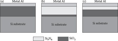
FIGURE 10.1 Schematic cross-sectional views of the three kinds of MIS structures: (a) MOS device: Al-SiO2(300 nm)-n-Si, (b) thick-oxide metal-nitride-oxide-semiconductor (MNOS) device: Al-SiO2 (200 nm)-Si3N4 (100 nm)-n-Si, and (c) thin-oxide MNOS device: Al-SiO2 (50 nm)-Si3N4 (250 nm)-n-Si.
The amount of trapped charge calculated from the change in the flat band voltage is just an approximation of the charge located in the bulk dielectric because the position of the trapped charges in the dielectric will affect the result. The charge near the Si/dielectric interface will contribute a larger C–V shift than the charges near the metal electrode due to there being more mirror charges in the semiconductor [10]. Even then, this method is still a good way to evaluate how charge accumulates in different dielectrics.
10.3.1 CHARGE INJECTION RESULTS
The C–V curves were measured for all the samples by performing a voltage sweep from −20 to 20 V and applying a small-signal AC voltage with a frequency of 100 kHz. Before applying a DC bias to the MIS device, C–V measurement on a virgin MIS device was carried out twice. This is to make sure that the sweep voltage does not influence the charge accumulation in the dielectric.
In all our experiments, to inject space charges into the dielectrics, the samples are electrically stressed by applying a DC bias for 1 min to the metal electrode of the MIS device. Then, to determine the charge accumulation before relaxation, C–V measurement is immediately performed after the DC bias is removed. In Figure 10.2a and c, the measured C–V curves for the three fabricated MIS devices before and after DC stress are shown.
For all the three samples shown in Figure 10.2, when the metal electrode is biased with low positive voltages (say 28 and 30 V), there was no obvious shift between the two C–V curves measured before and after DC stress. This indicates that the net injected charge in the dielectric of the sample device is negligible. In contrast, when the applied voltage increases to 32 V or more, the obtained C–V curve shifts indicate that the number of charges injected into the dielectric of the three devices is considerable and cannot be neglected. The results can be explained as follows.
For a thick dielectric layer, there exists a critical electric field that can determine whether significant charge tunneling will take place or not. If the applied electric field is lower than the critical value, the dominant conduction mechanism is ascribed to temperature-dependent Schottky emission, which takes place significantly only at high temperature [11] and is negligible at room temperature [12]. Therefore, there was no significant C–V curve shift for the three devices at low bias voltage such as 28 and 30 V because the measurement is performed at room temperature. Once the electric field is over the critical value, Fowler–Nordheim (FN) tunneling through a triangular barrier begins to dominate the charge injection [13]. The tunneling probability depends exponentially on the tunneling barrier height, the effective mass of tunneling carriers, and the electric field across the dielectric. This conduction mechanism dominates over Schottky emission at room temperature under a high electric field. Therefore, C–V curve shifts were observed when the applied voltages increased to 32 V.
Moreover, the measured C–V curves for the three samples shift in different directions. For the MOS device shown in Figure 10.2a, the shift is to the right side, indicating that net negative charges were injected into the silicon oxide film. A similar result is also found for the thin oxide MNOS device. In this case, the amount of net charges and their polarity is mainly attributed to the injection of charges with the same polarity as the potential of the Si substrate.
However, for the thick oxide MNOS device, as shown in Figure 10.2b, the C–V curve shifted to the left side when the metal electrode is biased with high positive bias voltage. This result indicates that net positive charges were accumulated in the dielectric of the thick oxide MNOS device. In this case, the amount of net charges and their polarity is mainly attributed to the injection of charges with the same polarity as the potential of the Al electrode.
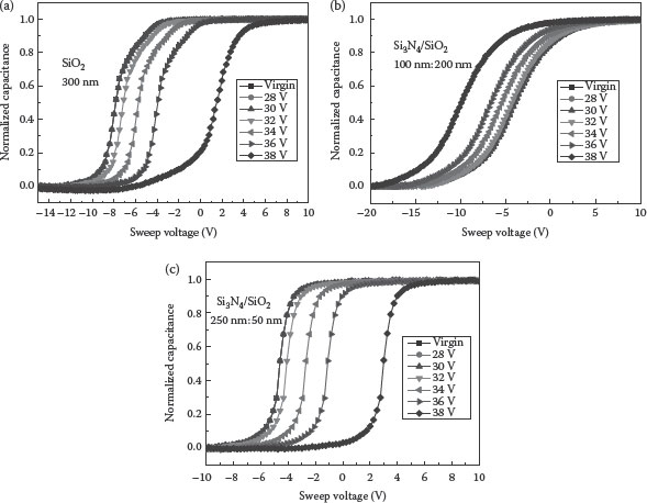
FIGURE 10.2 Measured C–V curves for the three MIS devices before and after the charge injection: (a) MOS device, SiO2 = 300 nm, (b) thick oxide MNOS device, Si3N4/SiO2 = 100 nm:200 nm, and (c) thin oxide MNOS device, Si3N4/SiO2 = 250 nm:50 nm. Positive DC bias voltages of 28, 30, 32, 34, 36, and 38 V at the metal electrode of MIS devices are applied for 1 min, respectively.
The experimental results in the MOS and the thin oxide MNOS devices show that an electron injection from the silicon substrate dominates the charge injection at high positive bias voltage. When a large positive bias is applied on the metal electrode of the MIS structure, the C–V curve shift benefits from both the electron injection from the semiconductor and a hole injection from the metal electrode into the dielectric, but the electron injection is the dominant injection mechanism that leads to negative charge accumulation in the dielectric [13,14]. However, this explanation cannot apply to the result obtained for the thick oxide MNOS device, in which the net positive charge accumulation was observed after the positive bias stress.
The experimental results suggest that the effects of both hole injection and electron injection should be taken into account when we analyze charge accumulation. To better understand the above-mentioned charge injection behavior, we have to investigate the charge transport mechanism in a general MIS capacitor structure under high bias voltage. In fact, charge transport in the insulator of an MIS capacitor structure under an electric field depends not only on the insulator itself but also on the interaction of the insulator with its contact electrodes [15,16]. Consequently, carrier conduction processes can be classified into two groups: (i) bulk-limited (Poole–Frenkel, ohmic, and space-charge-limited) conduction and (ii) electrode-limited (Schottky and Fowler–Nordheim) conduction [17].
The electrode-limited conduction corresponds to the charge injection into the dielectric from the contact interfaces. Schottky emission, as shown in Figure 10.3, is the temperature-induced flow of charge carriers that passes over a potential-energy barrier into the conduction band. This takes place significantly if the temperature is high enough and the electric field is lower than about 108 Vm−1. FN tunneling is known as a temperature-independent charge transfer mechanism, which is applied to a triangular barrier and takes place when the barrier thickness is relatively large [18]. In our case, the FN tunneling mechanism is important as an electrode-related process because the dielectric layer is relatively thick (about 300 nm) and the electric field in the dielectric is relatively high.
The bulk-limited conduction is related to the charge-trapping process in the dielectric after charge injection. Poole–Frenkel conduction was observed to be the dominant conduction mechanism [19]. The electrode-limited conduction happens before the subsequent bulk-limited conduction, and charge conduction in the bulk dielectric is very difficult to control, which involves the modification of the electrical properties of the dielectric materials, while the electrode-limited conduction can be easily modified, such as by changing the work function of the electrode. We focus on the electrode-limited conduction for the purpose of modifying the charge accumulation in the dielectric in this work.
In Figure 10.3, and later figures, the tunneling barriers are shown as exactly triangular. In reality, the barriers are rounded and reduced in strength by image-force effects [26]. In the simplified mathematical analysis that follows, we treat the barriers as exactly triangular. This does not affect the qualitative validity of our results. More generally, we simplify the influence of bulk-limited conduction on charge-trapping process, and assume the bulk of dielectric as a black box where charge trapping happens during the process of the charge carriers tunneling through the insulator. Specifically, it is assumed that any differences in the rates of electrons and holes supply to the interface may be neglected, and that the charge trapped in the dielectric as a result of a particular injection process is proportional to the typical tunneling probability for that injection process.
According to the above arguments, the processes of charge injection and their trapping in the SiN film of MIS structure under high stress voltage can be described by a modified FN tunneling charge injection model (see Figure 10.4). In the model, we assume that both the electron injection from the grounded electrode and the hole injection from the positively biased electrode contribute to the charge injection. Thus, in this model, the amount of trapped charge relates to the FN tunneling probabilities. The FN tunneling probability for a triangular barrier is given by the well-known Wentzel–Kramer–Brillouin (WBK) approximation [20,21].
(10.1) |
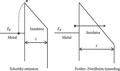
FIGURE 10.3 Energy diagram of Schottky emission and Fowler–Nordheim tunneling.
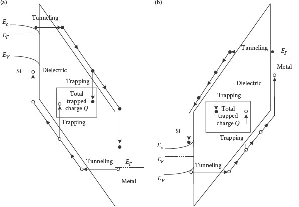
FIGURE 10.4 Modified Fowler–Nordheim (FN) tunneling energy diagram of a general Si/dielectric/metal structure: (a) with a positive stress voltage at the metal electrode, and (b) with a negative stress voltage at the metal electrode.
where ℏ is the Planck’s constant, m* is the effective mass of the tunneling carrier, q is the charge of the electron, ϕ is the barrier for the tunneling carrier, and E is the effective electric field inside the dielectric. From this equation, the effective masses of the tunneling carriers, injection barrier, and the electric field are important parameters that will influence charge injection in the dielectric under high applied voltage.
Based on Equation 10.1, for positive stress voltage (voltage on Al is positive relative to Si), the amount of trapping holes is proportional to the tunneling probability of holes from the Fermi level of metal to the dielectric and can be expressed as
(10.2) |
where Ne is the number of trapped electrons in the dielectric, Pe is the tunneling probability of electrons, me* is the effective mass of the tunneling electron, Ee is the electric field strength in the dielectric in which electrons tunnel into, and ϕe is the barrier height for electron tunneling. Similarly, the tunneling probability of electrons from the valence band of the silicon semiconductor to the dielectric can be expressed as
(10.3) |
where Nh is the number of trapped holes in the dielectric, Ph is the tunneling probability of electrons, mh* is the effective mass of tunneling holes, Eh is the electric field strength in the dielectric in which holes tunnel into, and ϕh is the barrier height for hole tunneling.
10.3.3 ANALYSIS OF RESULTS AND DISCUSSION
Based on Equation 10.1, the charge accumulation behavior at high bias voltage will now be analyzed. The key parameters are the effective masses of the tunneling carriers m*, the injection barrier ϕ, and the electric field strength E in the dielectric. Using Equations 10.2 and 10.3, the ratio of tunneling probabilities may be formed.
(10.4) |
From Equation 10.4, we see that Pe < Ph if r > 1 and Pe > Ph when r < 1. Thus we can use the parameter r to predict the polarity of the accumulated charge. For the MOS device, the electric field strength is the same for charge injection of both electrons and holes. For the MNOS device, the electric field strengths are different for electron and hole charge injections due to the different dielectric constants of SiO2 and Si3N4. To calculate the field strengths EO in SiO2 and EN in Si3N4, we model the double-layer dielectric as two parallel capacitors in series. Charge conservation then gives
(10.5) |
where Cox and CN are the capacitances formed by SiO2 and Si3N4 films in the MNOS structure, and Vox and VN are the voltage drops across the SiO2 and Si3N4 films, respectively. Then Equation 10.5 gives
(10.6) |
where εox and εN are the effective dielectric constants of SiO2 and Si3N4 films, and dox and dN are the thickness of SiO2 and Si3N4 dielectric films, respectively. The ratio of the electrical field strengths for hole and electron tunneling is then
(10.7) |
The parameter r is then conveniently given by known material properties as
(10.8) |
We use the typical dielectric constant of PECVD SiO2 εox = 4.2 ε0 and Si3N4 εN = 7.0ε0. Then, based on Equation 10.8, we can make Table 10.1.
In the case of the MOS device, the band gap Eg of silicon dioxide is 8.1 eV as shown in Figure 10.4. When the metal electrode is positively biased, the potential barrier of silicon dioxide for the hole injection from the Al electrode is higher than the barrier for the electron injection from the silicon substrate.
Thus, from the estimation given in Table 10.1, we get Pe > Ph, which concludes that the electron injection from the silicon substrate will dominate the charge injection. This result complies with the experimental result in Figure 10.2a, that is, electrons accumulate in the SiO2 film.
The tunneling barrier heights in the MNOS device are shown in Figure 10.5 when the metal electrode is positively biased.
TABLE 10.1
Estimated Tunneling Parameters
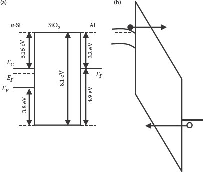
FIGURE 10.5 (a) Energy diagram of metal-SiO2 (200 nm)-Si3N4 (100 nm)-n-Si (thick oxide MNOS) device without bias voltage at the metal electrode. (b) Modified Fowler–Nordheim tunneling when the metal electrode is positively biased.
For the thick oxide MNOS device shown in Figure 10.6, the estimates in Table 10.1 give Ph > Pe, which concludes that the hole injection from the Al electrode will dominate the charge injection. This result also complies with the experimental result in Figure 10.2a.
Similarly, for the thin oxide MNOS device shown in Figure 10.7, we still get Ph > Pe, which also indicates that the hole injection from the Al electrode will dominate the charge injection in the thin oxide MNOS device. However, the experimental result shows that the electron injection from the silicon substrate dominates the charge injection. The predicted result based on the simple model estimate is in conflict with the experimental result in Figure 10.2c. This suggests that the charge injection mechanism in the double-layer dielectric should be more complicated.
A possible explanation for this discrepancy can be as follows: It is well known that the SiO2/Si3N4 interface has a much higher trap density than the bulk of SiO2 or Si3N4. These interface traps are more easily charged or discharged if the distance from this interface to the substrate is small [27].
Therefore, the thickness of SiO2 between the silicon nitride and the silicon surface will strongly affect the charge accumulation behavior in the MNOS structure. If the thickness of the SiO2 is thin, the electron injection will be enhanced due to the small distance from the SiO2/Si3N4 interface to the electron injection interface, as shown in Figure 10.7. This can be understood as a kind of trap-assisted tunneling [28]. In such a case, the SiO2/Si3N4 interface traps have a high possibility to capture the injected electrons instead of holes because this interface is too far to be reached for the hole injection from the Al electrode. As a result, the electron injection dominates the charge injection.
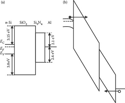
FIGURE 10.6 (a) Energy diagram of metal-SiO2 (200 nm)-Si3N4 (100 nm)-n-Si (thin oxide MNOS) device without bias voltage at the metal electrode. (b) Modified Fowler–Nordheim tunneling when the metal electrode is positively biased.
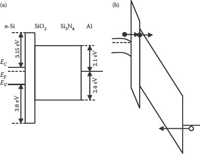
FIGURE 10.7 (a) Energy diagram of metal-SiO2 (50 nm)-Si3N4 (250 nm)-n-Si (thin oxide MNOS) device without bias voltage at the metal electrode. (b) Modified Fowler–Nordheim tunneling when the metal electrode is positively biased.
From the above experimental and modeling results, it follows that the tunneling barrier heights for electrons and holes in a given MIS structure are very important parameters to evaluate charge injection behavior, which will change as the dielectric changes. The effects of SiO2 thickness on charge accumulation in the Si3N4/SiO2 stacked dielectric may make it possible to balance the number of injected charges from the top and bottom electrodes by optimizing the thickness ratio of Si3N4 to SiO2.
This work demonstrates an investigation of charge accumulation in Si3N4/SiO2 dielectric stacks in comparison with that in a single-layer SiO2 dielectric for the purpose of controlling dielectric charging to improve the reliability of electrostatically actuated NEMS/MEMS membrane devices. The behavior of charge accumulation in the dielectric has been investigated by performing C–V measurements on an MIS capacitor structure. To explain the observed experimental results, we basically proposed a balance of holes and electrons from a modified FN limited charge injection model in combination with the interface trap-assisted tunneling. It is demonstrated that the sign of the charge accumulated in the MNOS devices can be controlled by the SiO2 thickness between the Si3N4 and the Si substrates. For the thin oxide MNOS structure, we attributed the negative charge accumulation to the enhancement of the electron injection from the silicon substrate, which is caused by the Si3N4/SiO2 interface trap-assisted tunneling due to lower distance from this interface to the electron injection interface. Conversely, the positive charge accumulation in the thick oxide MNOS structure was assumed to come from the suppression of the electron injection because the oxide is too thick to allow the interface trap-assisted tunneling.
1. U. Zaghloul, B. Bhushan, G. Papaioannou, F. Coccetti, P. Pons, and R. Plana, Nanotribology-based novel characterization techniques for the dielectric charging failure mechanism in electrostatically actuated NEMS/MEMS devices using force-distance curve measurements, J. Colloid Interface Sci., 365, 236, 2012.
2. H. San, Z. Deng, Y. Yu, G. Li, and X. Chen, Study on dielectric charging in low-stress silicon nitride with the MIS structure for reliable MEMS applications, J. Micromech. Microeng., 21, 125019, 2011.
3. C.L. Goldsmith, J. Ehmke, A. Malczewski, B. Pillans, S. Eshelman, Z. Yao, J. Brank, and M. Eberly, Lifetime characterization of capacitive RF MEMS switches, IEEEMTT-S Int. Microwave Symp. Digest, p. 227, 2001.
4. W. M. van Spengen, R. Puers, R. Mertens, and I. DeWolf, A comprehensive model to predict the charging and reliability of capacitive RF MEMS switches, J. Micromech. Microeng., 14, 514, 2004.
5. M. Exarchos, V. Theonas, P. Pons, G. J. Papaioannou, S. Melle, D. Dubuc, F. Cocetti, and R. Plana, Investigation of charging mechanisms in metal-insulator-metal structures, Microelectron. Reliab., 45, 1782, 2005.
6. G.J. Papaioannou, M. Exarchos, and V. Theona, Effect of space charge polarization in radio frequency microelectromechanical system capacitive switch dielectric charging, Appl. Phys. Lett., 89, 103512, 2006.
7. K. Seshan, Handbook of Thin-Film Deposition Processes and Techniques: Principles, Methods, Equipment and Applications (2nd ed), Noyes Publications/William Andrew Publishing, New York, 2002.
8. M. J. Madu, Fundamentals of Microfabrication: The Science of Miniaturization (2nd ed), CRC Press, Boca Raton, FL, 2002.
9. R.W. Herfst, P. G. Steeneken, and J. Schmitz, Time and voltage dependence of dielectric charging in RF MEMS capacitive switches, 45th Annual International Reliability, p. 417, 2007.
10. H. Krause, Electron injection and trap filling in insulating layers, Phys. Status Solidi A, 36, 705, 1976.
11. K.H. Ahn and S. Baik, Significant suppression of leakage current in (Ba,Sr)TiO3 thin films by Ni or Mn doping, J. Appl. Phys., 92, 5, 2002.
12. K.L. Ngai and Y. Hsia, Empirical study of the metal-nitride-oxide-semiconductor device characteristics deduced from a microscopic model of memory traps, Appl. Phys. Lett., 4, 159, 1982.
13. K. Lehovec, C. H. Chen, and A. Fedotowsky, MNOS charge versus centroid determination by staircase charging, IEEE Trans. Electron Devices, 25, 1030, 1978.
14. A.K. Agarwal and M. H. White, New results on electron injection, hole injection, and trapping in MONOS nonvolatile memory devices, IEEE Trans. Electron Devices, 32, 941, 1985.
15. T.C. McGill, S. Kurtin, L. Fishbone, and C. A. Mead, Contact-limited currents in metal-insulator-metal structures, J. Appl. Phys. 41, 3831, 1970.
16. J.G. Simmons, Conduction in thin dielectric films, J. Phys. D Appl. Phys., 4, 613, 1971.
17. A. I. K. Choudhury, M. R. R. Mazumder, K. Z. Ahmed, and Q. D. M. Khosru, Explanation for reduced Fowler–Nordheim tunneling current in ultra-thin silicon nitride gate dielectric, 3rd ICECE, Dhaka, Bangladesh, p. 2714, 2004.
18. J.G. Simmons, Poole–Frenkel effect and Schottky effect in metal-insulator-metal systems, Phys. Rev., 155, 657, 1967.
19. E.H. Rhoderick, Metal-Semiconductor Contacts, Clarendon, Oxford, 1978.
20. M.H. White and C. C. Chao, Statistics of deep-level amphoteric traps in insulators and at interfaces, J. Appl. Phys., 57, 2318, 1985.
21. D. Bohm, Quantum Theory, Prentice-Hall, Inc., Englewood Cliffs, 1951.
22. A.V. Vishnyakov, Y. N. Novikov, V. A. Gritsenko, and K. A. Nasyrov, The charge transport mechanism in silicon nitride: Multi-phonon trap ionization, Solid-State Electron., 53, 251, 2009.
23. M.I. Vexler, S. E. Tyaginov, and A. F. Shulekin, Determination of the hole effective mass in thin silicon dioxide film by means of an analysis of characteristics of a MOS tunnel emitter transistor, J. Phys. Condens. Matter, 17, 8057, 2005.
24. B. Brar, G. D. Wilk, and A. C. Seabaugh, Direct extraction of the electron tunneling effective mass in ultrathin SiO2, Appl. Phys. Lett., 69, 2728, 1996.
25. T. Maruyama and R. Shirota, The low electric field conduction mechanism of silicon oxide-silicon nitride-silicon oxide interpoly-Si dielectrics, J. Appl. Phys., 78, 3912, 1995.
26. S. Makram-Ebeid and M. Lannoo, Quantum model for phonon-assisted tunnel ionization of deep levels in a semiconductor, Phys. Rev. B, 25, 6406, 1982.
27. H. Castán, S. Dueñas, H. García, A. Gómez, L. Bailón, M. Toledano-Luque, A. del Prado, I. Mártil, and G. González-Díaz, Effect of interlayer trapping and detrapping on the determination of interface state densities on high-k dielectric stacks, J. Appl. Phys., 107, 114104, 2010.
28. K.A. Nasyrov, S. S. Shaimeev, and V. A. Gritsenko, Trap-assisted tunneling hole injection in SiO2: Experiment and theory, J. Exp. Theor. Phys., 109, 786, 2009.