
CONTENTS
Renewable energy sources, like hydroelectric power, wind power, tidal power, and photovoltaics, have great importance for satisfying the global demand for energy in the future, since the resources of fossil fuels are limited and nuclear power plants can be hazardous radiation sources for thousands of years if the outer shell is damaged. Photovoltaics is one of the most promising energy sources because the solar power density that reaches the earth can be as large as 136 mW/cm2 [1] and will continue to be available for millions of years. The state-of-the-art commercial Si solar cells are autarkic power plants, but they have the drawbacks of a relatively small conversion efficiency, the need for a high-temperature manufacturing process, and the fact that the use of strong chemicals during the fabrication process cannot be avoided. Further, the absorption range of Si solar cells is limited by the large bandgap of Si, so that Si solar cells cannot convert the infrared radiation produced by the sun [3]. These drawbacks can be overcome by utilizing the arrays of nano antennas, either as individual devices for energy harvesting or in combination with organic or inorganic solar cells as hybrid photovoltaic devices to extend the absorption spectrum and thus increase the total efficiency [4, 5 and 6]. The antenna length is usually set to several micrometers corresponding to the infrared regime, so that the antennas can be easily fabricated by optical lithography. The main challenge in the fabrication process of nano antenna arrays is therefore the implementation of a large number of terahertz rectifying devices, which are required to convert the terahertz alternating current induced in the antennas by the infrared radiation into a direct current. Efficient rectifiers, such as pn-junctions or Schottky diodes, cannot be used in this application, since the cutoff frequency of these devices is usually in the megahertz or at the best in the gigahertz range [7]. Recently, Schottky diodes with a cutoff frequency of a few terahertz have been reported [8], but only in the form of individual diodes that cannot be scaled to arrays consisting of millions of such devices. More promising are the metal–oxide–metal (MOM) junctions featuring a thin oxide layer with a thickness in the range of a few nanometers and with metals of different work functions. Such MOM junctions work as tunneling diodes, since the junctions exhibit asymmetric I–V characteristics with respect to the polarities of terahertz (THZ) alternating currents, owing to the fact that electrons tunnel through the thin barrier within femtoseconds [9,10]. However, this is true only if the area of the MOM junction is in the nanometer range, and therefore, simple conventional optical lithography is not applicable for the fabrication of nano antenna arrays, including MOM tunneling diodes. So far, single antenna-coupled MOM diodes (ACMOMDs) fabricated by electron-beam lithography and liftoff techniques have been reported and have shown a promising performances [11,12]. However, these devices have two main drawbacks. The first drawback is that the tunneling dielectric is obtained by the natural oxidation of an aluminum layer, resulting in an insulator with a thickness of 2–3 nm. The advantage of this fabrication method is its simplicity, but this oxide has poor reproducibility and poor electrical stability, resulting in a large fraction of shorted diodes. As an alternative to natural oxidation, a plasma-induced oxide growth has the advantage that it is far more reproducible, that the thickness of the oxide is limited to 3.6 nm, and that the physical properties of this oxide, such as its compactness, result in a dielectric that is electrically stable at high electrical fields. The second drawback of fabricating MOM diodes by electron-beam lithography is that this process is very time-consuming, which is problematic when fabricating arrays of millions of nano antennas. A more promising fabrication technique is the direct transfer-printing of complete arrays of nano antennas and MOM-rectifying diodes. Stacks of several metals are deposited onto a pretreated stamp having nanometer-size structures and are then transfer-printed onto a target substrate, which may consist of Si, SiO2, glass, or other materials [2]. Ultrathin dielectrics with a thickness of a few nanometers can also be fabricated and transferred in this way. The stamp can be either a soft stamp (e.g., polydimethylsiloxane, PDMS) or a hard stamp (e.g., silicon). Hard stamps have the advantages of providing higher resolution of the printed structures and the possibility of reusing the stamps several tens of times, provided the stamps are properly cleaned after each transfer step.
The basic process steps of the nanotransfer-printing process are given here. The main challenge that has to be overcome is the adhesion force. Since the materials that are to be transferred onto the target substrate have to be easily delaminated from the stamp, the surface energy of the stamp has to be reduced as much as possible. In contrast, the adhesion between the surface of the materials to be transferred and the target substrate has to be as strong as possible to guarantee a successful transfer. The surface energy of the stamp can be reduced by applying a hydrophobic molecular self-assembled monolayer (SAM). A material with a poor adhesion, ideally a noble metal, such as gold or platinum, providing very weak adhesion due to the small reactivity of noble metals, is deposited onto the hydrophobic stamp surface so that the adhesion between the stamp and the material stack is further decreased. After that, the MOM stack of the rectifying tunneling diodes is deposited, including the thin insulator. The last layer deposited onto the stamp should be an adhesion promoter to achieve a large adhesion force between the material stack to be transferred and the surface of the target substrate. Here, chromium or titanium is the material of choice. They can be further activated by a plasma treatment, which results in the formation of hydrophilic hydroxyl groups on the metal surface. Prior to the transfer-printing process, the target substrate is activated depending on the material it is made of. For example, the density of hydroxyl groups on the surface of a silicon substrate can be greatly increased by an RCA 2 (at 75°C) or a piranha clean. A plasma treatment results in a hydrophilic surface as well [13]. The density of hydroxyl groups on the activated silicon surface increases up to 5 OH/nm2 [14]. A silicon substrate covered with a thermally grown silicon dioxide layer needs a 1 min RCA 1 clean prior to a plasma treatment to achieve a hydrophilic surface [15]. Glass can be activated by a plasma treatment. After activating the target substrate, the stamp is placed on top of the target substrate and placed into an imprinting machine. Typical pressures that are applied are in the range of several tens of bars up to 1 kbar, depending on the printing machine. After demolding, the material stacks located on the elevated regions of the stamp are transfer-printed onto the target substrate and the stamp can be “recycled” by removing the metals remaining on the stamp by wet etching. In this way, hard stamps can be used several tens of times. An overview of the printing process is shown in Figure 11.1.
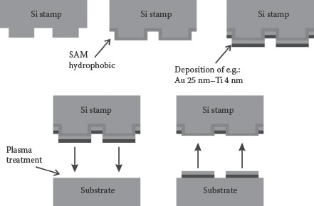
FIGURE 11.1 Basic steps of a nanotransfer-printing process: A Si stamp is covered by a hydrophobic self-assembled monolayer (SAM). After that, a noble metal (here Au) is deposited as the initial metal layer. To provide a good adhesion, the last metal layer consists of an adhesion promoter, which is Ti here. After a plasma treatment, the stamp and the substrate are brought into contact and the metal stacks on the elevated structures on the stamp are transferred onto the target substrate.
Two main fabrication methods exist for producing hard stamps, namely, molecular beam epitaxy (MBE) and e-beam lithography, both of which are described here.
Under economic aspects, the fabrication of MBE stamps lacks in cost-effectiveness, even if the stamps are “recycled.” However, stamp feature sizes down to a few nanometers can be achieved by MBE, since the epitaxially grown layer thicknesses can be controlled on the scale of a single atomic layer. A superlattice of AlGaAs and GaAs is grown lattice-matched on a 2 in GaAs wafer, which has a thickness of 300 μm. The Al content in the superlattice must be around 80% with respect to the other group III element to achieve a sufficient etching selectivity between GaAs and AlGaAs. A 5 mm × 8 mm piece is cut out of the wafer, and then the vertical side edges of the wafer piece are selectively etched using citric acid or HF. Citric acid selectively removes GaAs with respect to AlGaAs, thus producing a side edge with three-dimensional features corresponding to the periodicity of the AlGaAs/GaAs superlattice, as shown in Figure 11.2. When etching the MBE stamp with HF (5%), AlGaAs is selectively etched, resulting in small gaps on the stamp. The etched MBE stamps are then either left in clean-room conditions for 1 day to allow the surface to oxidize or covered with a hydrophobic SAM featuring a thiol group, such as n-octanethiol. When depositing metals onto an MBE stamp, this hydrophobic layer serves as a delaminating layer, so that the adhesion between the deposited metals and the stamp is weak; thus, the metals can be removed easily from the stamp. A gold layer with a thickness of 15–45 nm is followed by a Ti layer with a thickness of 4 nm, which serves as an adhesion promoter, then deposited by thermal evaporation onto the patterned stamp. A layer of TiO2 is formed by allowing the surface of the Ti layer to oxidize. In general, TiO2 does not feature a highly hydrophilic surface; therefore, an oxygen-plasma treatment for several minutes destroys the titanium oxide bonds, and by exposing the stamp to air, hydrophilic hydroxyl groups are formed on the Ti/TiO2 surface. Silanols are formed on the Si target substrate (either with or without a layer of SiO2). The hydrophilic character of a bare Si surface is stable for several hours; however, in the case of an SiO2 surface, a reactivation of the surface is necessary after approximately half an hour. After activating the Ti on the stamp and the SiO2 on the substrate, both the stamp and the substrate were brought into contact and the 200-nm-thick Au/Ti lines were transferred onto the Si substrate. The custom-made MBE printing machine, as well as the nanotransfer process, is described elsewhere [16]. MBE stamps with structures down to 30 nm have been fabricated, leading to transferred Au lines with widths down to 43 nm. Other metals like aluminum have also been transferred. In a subsequent process step, the printed lines can be adjusted to the antenna length of several micrometers via a focused ion beam (FIB).
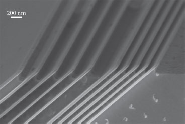
FIGURE 11.2 Scanning electron microscopy (SEM) image of a stamp produced by molecular beam epitaxy with feature sizes as small as 30 nm.
So far, we have presented an unconventional method for the fabrication of hard stamps with small feature sizes and MBE resolution. However, to cover large areas with structures in a single printing step, planar Si stamps must be considered more useful than stamps that consist only of the 300 μm wide edge of a wafer piece. Using electron-beam lithography followed by dry etching, the surface of an Si stamp can be patterned into any desired features with a resolution of approximately 45 nm over areas up to several square centimeters. To render the surface of the Si stamp hydrophobic and obtain low adhesion between the stamp surface and the deposited metals, the stamp is covered with an organic silane-based SAM, for example, 1H,1H,2H,2H-perfluorooctyltrichlorosilane [17]. The subsequent steps of covering the stamp with materials to be transferred to the target substrate are analogous to the MBE stamp process.
As discussed above, the microscale and nanoscale MOM tunneling diodes have been fabricated in a nanotransfer-printing process. For the microscale diodes [18], a planar Si wafer comprising a silane-based hydrophobic SAM served as the stamp. A stack of 10 nm thick Au, acting as a delamination layer between the diodes and the stamp, followed by a 20 nm thick Al layer, was deposited by thermal evaporation onto the stamp through a shadow mask, resulting in parallel metal lines on the substrate. The width of the lines ranged from 10 to 200 μm. After the metal deposition, a natural oxygen layer formed spontaneously on the Al surface upon exposure to air. As discussed above, the spontaneously grown aluminum oxide layer does not provide a compact and pure insulator. Therefore, an oxygen-plasma treatment was performed to increase the thickness of the aluminum oxide from ~1.6 nm to ~3.6 nm, resulting in a pure and compact AlOx layer [19,20]. After that, a 30 nm thick layer of Au, followed by 4 nm thick Ti acting as an adhesion layer between the MOM diodes and the target substrate, was evaporated through a second shadow mask, resulting in metal lines arranged perpendicular to the first set of metal lines. The active area of the microscale MOM diodes defined at the intersections of the two metal stacks ranges from 10−6 cm2 to 10−4 cm2.
Nanoscale MOM tunneling diodes were also fabricated using a flat Si stamp with pillars having a diameter of 50 nm [2]. The first layer that was deposited onto the stamp was 15 nm of AuPd (delamination layer). AuPd was chosen since it provides a very small surface roughness because of its small grain size. This is important in the nanometer regime because materials with rough surfaces are more difficult to transfer, since the contact area between the material to be transferred and the target substrate is very small. Then a 25 nm thick layer of Al (first electrode) was deposited and its surface oxidized by an oxygen-plasma treatment to obtain the tunneling dielectric, followed by the deposition of a 20 nm thick layer of AuPd as the second electrode. 4 nm of Ti serves again as an adhesion promoter. After activating the stamp and the target substrate to create hydrophilic surfaces, the completed microscale diodes are then transfer-printed onto an Si wafer covered with a 200 nm thick SiO2 layer, whereas the nanoscale diodes were transfer-printed onto an Si wafer covered with a conductive layer of 25 nm of AuPd, which has a layer of 4 nm of Ti on top to provide good adhesion to the materials to be transferred. The printing process has been carried out on an NIL-2.5 Nanoimprinter from Obducat. The pressure during transfer was 50 bar and it was held for 5 min. The temperature was set to 200°C, which is necessary to remove the water formed during the transfer process. The titanol surface groups from the stamp and the silanol surface groups from the target substrate react to a titansiloxane group and water is released. As this reaction is reversible, the removal of water is important. This is one reason why hard stamps, such as GaAs or Si, are more suitable than soft PDMS stamps [21, 22 and 23], which cannot withstand high temperatures, although it has also been shown in the literature that temperatures around 50°C improve the transfer process when using soft stamps [24].
A scanning electron microscope (SEM) and a probe station were used to characterize transfer-printed antenna structures fabricated with an MBE stamp. We have been able to show that the antenna structures are continuous over a length of almost 2 mm. By optical lithography and a liftoff process, the resistivity of the ensemble of transferred lines consisting of aluminum was determined to have a value of 2.3 × 10⁻⁸ Ω m, which is similar to the bulk resistivity of aluminum [25].
Antenna structures fabricated in a transfer-printing process using a flat Si-stamp were also characterized by SEM. The Au lines are continuous over an area of 0.6 mm × 0.6 mm, but larger areas can also be covered. The transfer yield is almost 100%, which is defined by the percentage of successfully transferred structures with respect to the structures on the stamp on which the materials were initially deposited. The morphology of the lines is excellent and even more complex structures like grid-like structures can be transferred when tailoring the printing parameters. Further processes on the transferred antenna structures can include optical lithography and lift-off, for example, to define contact pads, or also more complex processes like FIB. With respect to liftoff processes, we want to point out that the adhesion of the Au lines to the substrate is high due to the Ti layer.
For the microscale transfer-printed MOM tunneling diodes, the transfer yield is also almost 100% [26]. Atomic force microscope (AFM) measurements of the MOM diodes on the stamp before printing and on the substrate after printing show that the heights are similar, which indicates that the morphology of the metal layers was not affected by the transfer process. To show that the ultrathin AlOx dielectric still works as an insulating layer after transfer, electrical measurements were performed using a probe station. Since the MOM diode represents the overlap of an Au/Al/AlOx line and a Au/Ti line, the electrical characterization could easily be done by contacting the two electrodes without touching or affecting the active area and especially the ultrathin dielectric. The I–V characteristics of the printed MOM tunneling diodes are presented in Figure 11.3a (symbols). The applied bias was varied on the Au electrode. Asymmetric I–V characteristics with respect to the polarities, as determined in the measurements, are essential; otherwise, the MOM junction would not represent an unbiased rectifying device. To show that direct (and Fowler–Nordheim) tunneling instead of, for example, trap-assisted tunneling, is the main current mechanism occurring in the MOM diodes, simulations were carried out using a kinetic Monte Carlo model [27,28] and numerical simulations [29]. Using these models, we have been able to not only validate this hypothesis but also show that transport in the diodes is dominated by electron tunneling. The current density can be described by the Tsu-Esaki formula [30]. For low voltages below 3.3 and 4.3 V for negative and positive biases, respectively, direct tunneling was observed and for higher voltages, Fowler–Nordheim tunneling was observed. However, in the initial Monte Carlo model, planar metal layers without any surface roughness were assumed. For currents below 5 × 10⁻⁴ A/cm2, the simulation fits the experimental data very well. However, for larger currents, the simulation does not match the experimental results. Here, the effects of the surface roughness of the insulator/electrode interface are important, especially for the electron injection into the aluminum electrode. The nonideal inhomogeneous distribution of the applied electric field was found to cause this derivation. By measuring the surface roughness of the Au/Al/AlOx layer with an AFM after transfer-printing (see Figure 11.3b), an root mean square (RMS) value of 0.5 nm over an interval of 20 nm was determined. The electric field at local height peaks on the surface is larger than on a planar metal layer. By including these effects in the Monte Carlo simulation, a better effect, especially for higher voltages, was achieved. A further parameter besides the tunneling barrier height of 3.3 eV for the Al/AlOx interface and 4.3 eV of the Au/AlOx interface that was assumed when taking the surface roughness of the interface into account is an effective electron tunneling mass of 0.35 m0, which is reasonable [31]. Since aluminum oxide is known to have a work function of around 1 eV, the measured values of the barrier heights are in good agreement with the theoretical values [18,26].
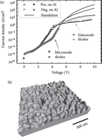
FIGURE 11.3 (a) Electrical characterization and simulations of a printed MOM tunneling diode. (Reprinted with permission from M. Bareiß et al., High-yield transfer printing of metal–insulator–metal nanodiodes, ACS Nano, 6, 2853–2859, 2012/03/27. Copyright 2012, American Chemical Society.) (b) Roughness of the Al/AlOx layer determined by AFM.
The morphological characterization of the MOM tunneling nanodiodes was achieved by SEM. Here, the transfer yield was also found to be excellent at 98%. The diameter of the transferred MOM pillars was found to increase from 50 to 94 nm, which results from the fact that during evaporation, the material was accumulated on the sidewalls of the previously deposited materials on the stamp. However, the electrical characterization of the nanodiodes is more challenging than that the microdiodes because, unlike the microdiodes, the nanodiodes cannot be contacted outside the active area. Therefore, for the characterization of the nanodiodes, a conductive atomic force microscope (C-AFM) was employed to make soft electrical contact to the top electrode, while the bottom electrode was connected via a clamp that was attached to the conductive substrate (see Figure 11.4). The I-V characteristics were determined only for voltages above 5 V since the noise introduced by the C-AFM setup did not permit the measurement of smaller voltages. The bias-dependent current densities measured in the nanodiodes are perfectly consistent with those measured previously in the microdiodes, which confirms the reliability of the materials and the fact that downscaling does not change the diode’s characteristics (Figure 11.3a). Note that very large electric fields can be applied to the nanodiodes without causing damage, which was not possible with the microdiodes. We believe that the reason is the fact that the number of potentially catastrophic defects scales with the diode area. Since all fabrication was carried out under clean-room conditions, the absolute defect number may even be practically zero over sufficiently small areas [2].
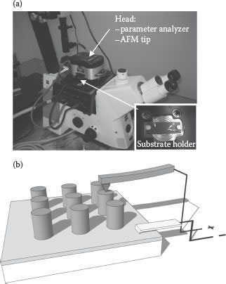
FIGURE 11.4 (a) A photograph of the conductive AFM setup: The parameter analyzer and the AFM tip are implemented in the head, and the substrate holder comprises a ceramic plate and gold clamps for connecting the sample substrate. (b) A schematic view of the AFM setup: The MIM pillars (vertical pillars) that are transfer-printed onto the Si target substrate coated with a conductive AuPd layer are contacted from the top via a conductive AFM tip (here positive potential). The AuPd layer on the substrate is connected via a gold clamp (here negative potential). (Reprinted with permission from M. Bareiß et al., High-yield transfer printing of metal–insulator–metal nanodiodes, ACS Nano, 6, 2853–2859, 2012/03/27. Copyright 2012, American Chemical Society.)
In summary, we demonstrated the transfer-printing of arrays of nano antenna structures using either an MBE stamp or a patterned Si stamp featuring an excellent morphology and reliable electrical resistivity. Microscale and nanoscale MOM tunneling diodes with an ultrathin dielectric of 3.6 nm of AlOx fabricated in an oxygen-plasma process were transfer-printed in a single printing step. The transfer yield is almost 100% and the electrical characteristics are in line with the Monte Carlo and numerical simulations.
The main challenge that we want to overcome in our future work is the implementation of a MOM nanodiode in an array of transfer-printed antennas on even larger areas to be suitable for energy-harvesting applications. Since the cutoff frequency of a MOM diode is dependent on its area, a further goal is the reduction of the area to values around 50 nm. Here, MBE stamps might be particularly well suited, since we already showed a successful transfer of Au lines having a width of 43 nm. A second, perpendicular transfer comprising Al and a thin layer of AlOx would create a nanoscale diode with a smaller area. This would expand the possible absorption spectrum into the high THz regime and could lead to higher energy absorption from sunlight.
The authors thank Rosi Heilmann for her invaluable help. The authors acknowledge the financial support from the German Research Funding (DFG) through the TUM International Graduate School of Science and Engineering (IGSSE) and the Institute for Advanced Studies (IAS), the focus group “Nanoimprint and Nanotransfer,” and the DFG Excellence Cluster “Nanosystem Initiative Munich.”
1. M.P. Thekaekara and A. J. Drummond, Standard values for the solar constant and its spectral components, Nat. Phys. Sci., 229, 6–9, 1971.
2. M. Bareiß, F. Ante, D. Kälblein, G. Jegert, C. Jirauschek, G. Scarpa, B. Fabel, E. M. Nelson, G. Timp, U. Zschieschang, et al., High-yield transfer printing of metal–insulator–metal nanodiodes, ACS Nano, 6, 2853–2859, 2012/03/27 2012.
3. S.S. Iyer and Y. H. Xie, Light emission from silicon, Science, 260, 40–46, 1993.
4. C. Fumeaux, W. Herrmann, F. K. Kneubühl, and H. Rothuizen, Nanometer thin-film Ni-NiO-Ni diodes for detection and mixing of 30 THz radiation, Infrared Phys. Technol., 39, 123–183, 1998.
5. C. Fumeaux, W. Herrmann, H. Rothuizen, P. De Natale, and F. K. Kneubühl, Mixing of 30 THz laser radiation with nanometer thin-film Ni-NiO-Ni diodes and integrated bow-tie antennas, Appl. Phys. B Lasers Opt., 63, 135–140, 1996.
6. I. Wilke, Y. Opplinger, W. Herrmann, and F. K. Kneubuhl, Nanometer thin-film Ni-NiO-Ni diodes for 30 THz radiation, Appl. Phys. A, 58, 329–341, 1994.
7. M. Bareiß, A. Hochmeister, G. Jegert, U. Zschieschang, H. Klauk, B. Fabel, G. Scarpa, W. Porod, and P. Lugli, Quantum carrier dynamics in ultra-thin MIM tunneling diodes, 17th International Conference on Electron Dynamics in Semiconductors, Optoelectronics and Nanostructures, EDISON 17, 2011.
8. S. Barbieri, J. Alton, C. Baker, T. Lo, H. Beere, and D. Ritchie, Imaging with THz quantum cascade lasers using a Schottky diode mixer, Opt. Express, 13, 6497–6503, 2005.
9. J.A. Bean, B. Tiwari, G. H. Bernstein, P. Fay, and W. Porod, Thermal infrared detection using dipole antenna-coupled metal-oxide-metal diodes, J. Vac. Sci. Technol. B, 27, 11–14, 2009.
10. J.A. Bean, A. Weeks, and G. D. Boreman, Performance optimization of antenna-coupled Al/AlOx/Pt tunnel diode infrared detectors, IEEE J. Quantum Electron., 47, 126–135, 2011.
11. B.A. Slovick, J. A. Bean, P. M. Krenz, and G. D. Boreman, Directional control of infrared antenna-coupled tunnel diodes, Opt. Express, 18, 20960–20967, 2010.
12. B. Tiwari, J. A. Bean, G. Szakmany, G. H. Bernstein, P. Fay, and W. Porod, Controlled etching and regrowth of tunnel oxide for antenna-coupled metal-oxide-metal diodes, J. Vac. Sci. Technol. B, 27, 2153–2160, 2009.
13. M. Bareiß, M. A. Imtaar, B. Fabel, G. Scarpa, and P. Lugli, Temperature enhanced large area nano transfer printing on Si/SiO2 substrates using Si wafer stamps, J. Adhes., 87, 893–901, 2011.
14. R.K. Iler, The Chemistry of Silica, Wiley, New York, 1979.
15. T. Suni, K. Henttinen, I. Suni, and J. Mäkinen, Effects of plasma activation on hydrophilic bonding of Si and SiO2, J. Electrochem. Soc., 149, G348–G351, 2002.
16. S. Harrer, S. Strobel, G. Scarpa, G. Abstreiter, M. Tornow, and P. Lugli, Room temperature nanoimprint lithography using molds fabricated by molecular beam epitaxy, IEEE Trans. Nanotechnol., 7, 363–370, 2008.
17. S.A. Kulinich and M. Farzaneh, Hydrophobic properties of surfaces coated with fluoroalkylsiloxane and alkylsiloxane monolayers, Surf. Sci., 573, 379–390, 2004.
18. M. Bareiß, A. Hochmeister, G. Jegert, U. Zschieschang, H. Klauk, R. Huber, D. Grundler et al., Printed array of thin-dielectric metal-oxide-metal (MOM) tunneling diodes, J. Appl. Phys., 110, 044316, 2011.
19. H. Ryu et al., Logic circuits based on individual semiconducting and metallic carbon-nanotube devices, Nanotechnology, 21, 475207, 2010.
20. U. Zschieschang, F. Ante, M. Schlörholz, M. Schmidt, K. Kern, and H. Klauk, Mixed self-assembled monolayer gate dielectrics for continuous threshold voltage control in organic transistors and circuits, Adv. Mat., 22, 4489–4493, 2010.
21. Y. -L. Loo, D. V. Lang, J. A. Rogers, and J. W. P. Hsu, Electrical contacts to molecular layers by nanotransfer printing, Nano Lett., 3, 913–917, 2003.
22. Y. -L. Loo, R. L. Willett, K. W. Baldwin, and J. A. Rogers, Interfacial chemistries for nanoscale transfer printing, J. Am. Chem. Soc., 124, 7654–7655, 2002.
23. J. Zaumseil, M. A. Meitl, J. W. P. Hsu, B. R. Acharya, K. W. Baldwin, Y. -L. Loo, and J. A. Rogers, Three-dimensional and multilayer nanostructures formed by nanotransfer printing, Nano Lett., 3, 1223–1227, 2003.
24. J.-h. Choi, K.-H. Kim, S.-J. Choi, and H. H. Lee, Whole device printing for full colour displays with organic light emitting diodes, Nanotechnology, 17, 2246–2249, 2006.
25. M. Bareiß, A. Hochmeister, G. Jegert, G. Koblmüller, U. Zschieschang, H. Klauk, B. Fabel, G. Scarpa, W. Porod, and P. Lugli, Energy Harvesting using Nano Antenna Array, Nanotechnology (IEEE-NANO), 2011 11th IEEE Conference on, pp. 218–221, 2011.
26. M. Bareiß, B. N. Tiwari, A. Hochmeister, G. Jegert, U. Zschieschang, H. Klauk, B. Fabel et al., Nano antenna array for terahertz detection, IEEE Trans. Microwave Theory Tech., 59, 2751–2757, 2011.
27. G. Jegert, A. Kersch, W. Weinreich, and P. Lugli, Monte Carlo simulation of leakage currents in TiN/ZrO2/TiN capacitors, IEEE Trans. Electron Devices, 58, 327–334, 2011.
28. G. Jegert, A. Kersch, W. Weinreich, U. Schroder, and P. Lugli, Modeling of leakage currents in high-kappa dielectrics: Three-dimensional approach via kinetic Monte Carlo, Appl. Phys. Lett., 96, 062113, 2010.
29. C. Jirauschek, Accuracy of transfer matrix approaches for solving the effective mass Schrödinger equation, IEEE J. Quantum Electron., 45, 1059–1067, 2009.
30. R. Tsu and L. Esaki, Tunneling in a finite superlattice, Appl. Phys. Lett., 22, 562–564, 1973.
31. W.Y. Ching and Y. -N. Xu, First-principles calculation of electronic, optical and structural properties of alpha-Al2O3, J. Am. Ceram. Soc., 77, 404–411, 1994.