
CONTENTS
13.2.1 Activation Procedure for Series-Connected Nanogaps
13.3.1 Tuning of Structural and Electrical Properties of Integrated Nanogaps by Activation
13.3.2 Integration of SETs Using Activation
The fabrication of large-scale, reproducible nanogap electrodes is a key issue for the integration of nanoscale devices such as single-electron transistors (SETs). SETs have been studied extensively because of their potential advantages in high integration density and low power consumption. There are many experimental reports on the fabrication techniques of metallic SETs, based on nanogaps with randomly placed nanoparticles [1, 2, 3, 4 and 5]. However, it is almost impossible to control the position of islands of SETs using these fabrication techniques. On the other hand, highly elaborate shadow evaporation [6,7] and scanning probe microscope (SPM)-based oxidation [8,9] have also been reported, and the fabrication methods have achieved a high-temperature operation of SETs. However, it is known that these approaches are complicated and require special techniques and systems.
Recently, the electromigration method, based on the electrical current-induced diffusion of metal atoms in a thin metal film, has been extensively investigated as a fabrication method of nanogaps (i.e., nanoscale electrodes with nanometer separation) [10, 11, 12, 13 and 14]. From the point of view of the integration of nanogaps, parallel fabrication of multiple nanogaps based on the electromigration method has already been reported by other researchers [15,16]. However, the electrical properties of individual nanogaps are not in situ measured in the method. In addition, the nanogap electrodes fabricated by the electromigration method generally have a tendency to exhibit high tunnel resistance. Hence, we consider that it is difficult to utilize this conventional electromigration procedure for the fabrication/integration of nanogaps with well-controlled tunnel resistance.
Over the past few decades, field emission phenomena have been widely utilized in vacuum microelectronics and extensively studied theoretically [17]. The current flowing through nanogaps is dominated by an electron-tunneling process leading to a high electric field. Such a field emission current also has a tendency to reconstruct the atomic geometry at the tip of the nanogap electrodes or even destroy the tip surface [18]. By utilizing such phenomena, we have reported a wide range of control over tunnel resistance of nanogaps by field-emission-induced electromigration, a technique called “activation” [19,20]. “Activation” is based on moving atoms induced by the Fowler–Nordheim (F–N) field emission current passing through the nanogaps. Using the activation procedure, we can control the electrical properties of the nanogaps by adjusting the magnitude of the preset current of the activation and easily obtain nanogap-based SETs [21]. Furthermore, we have also demonstrated the integration method of two SETs with similar electrical properties by using the activation procedure, and the charging energy of the two SETs can be simultaneously controlled by the preset current in the activation [22,23]. Consequently, it is considered that the electrical properties of tunneling devices based on nanogaps can be tuned by adjusting the magnitude of the preset current during the activation procedure. In this chapter, we present a remarkably simple and easy technique for the simultaneous tuning of tunnel resistance of three nanogaps connected in series using the activation procedure. Furthermore, a reproducible method based on the activation scheme is also reported in detail for the fabrication/integration of planar-type nanogap-based SETs.
13.2.1 ACTIVATION PROCEDURE FOR SERIES-CONNECTED NANOGAPS
The fabrication and activation procedures of the samples are composed of two main steps. First, we fabricated the initial Ni nanogaps by electron-beam (EB) lithography, EB deposition, and lift-off process on thermally oxidized silicon substrates. In this study, we use multiple initial Ni nanogaps connected in series. The tip shape of the nanogaps is sharpened in order to produce a field emission current caused by electric field concentration at the tip of the nanogap electrode.
In the next step, the activation experiments were carried out in a vacuum chamber using a semiconductor parameter analyzer. During the activation, the field emission current I was simultaneously applied to the initial nanogaps connected in series in current source mode. The activation process is performed as follows (Figures 13.1a,13.1b, and 13.1c). First, we set the preset current IS. Then F–N field emission current is induced in the series-connected Ni nanogaps. Since the three nanogaps are connected in series (Figure 13.1a), an identical field emission current passes through each nanogap device during the activation procedure. It should be noted that the activated atoms induced by the F–N field emission current, which is completely controlled by the current source, are just moved from the source to the drain electrode when the voltage drop across the nanogap is suddenly decreased. Thus, the sample with wider initial gap separation is preferentially and immediately narrowed by the field emission current with a higher voltage drop (Figure 13.1b), and the applied current I is slowly ramped up until it reaches the preset current IS. As a result, it is considered that the electrical properties of the activated nanogaps become similar to each other, with the progress of the activation (Figure 13.1c). In other words, the gaps of the series combination of the three Ni nanogap electrodes can self-regulate with final spacing set by the applied current. After performing the activation, ID–VD properties of each nanogap were measured individually. This procedure was continuously repeated while increasing the preset current IS from 1 nA to 30 μA. The advantage of this fabrication method is that nanogaps having similar electrical properties can be simultaneously formed because the magnitude of the field emission current becomes the same in each nanogap. Hence, it is strongly suggested that the simultaneous tuning of nanogaps can be achieved simply and easily by just passing a field emission current through a large number of nanogaps connected in series.
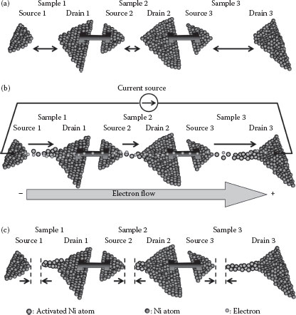
FIGURE 13.1 Schematic representation of the integration process during activation. (a) Three initial nanogaps with a separation of a few tens of nanometers are defined by conventional electron-beam lithography and lift-off process. (b) An identical field emission current passes through each device during the activation procedure. Then the sample with the wider initial gap separation is preferentially and immediately activated by the field emission current with a higher voltage drop. (c) Nanogaps having similar electrical properties can be simultaneously formed, because the gaps self-regulate with final spacing set by the applied current.
13.3.1 TUNING OF STRUCTURAL AND ELECTRICAL PROPERTIES OF INTEGRATED NANOGAPS BY ACTIVATION
The activation with a current source was performed to simultaneously control the multiple planartype series-connected Ni nanogaps at room temperature. Scanning electron microscopy (SEM) images of samples A-1, A-2, and A-3 before performing the activation are shown in Figures 13.2a–c, respectively. In the SEM images, initial gap separation of the samples A-1, A-2, and A-3 is estimated to be approximately 114, 80, and 108 nm, respectively. The initial nanogaps showed high tunnel resistance above 100 TΩ, which clearly reflects the initial gap separation of the samples. On the other hand, after performing the activation with the preset current IS of 30 μA, the separation of the gaps was reduced to less than 10 nm, which is due to the accumulation of Ni atoms at the tip of each drain electrode, as shown in Figures 13.2d–f.
Figure 13.3a shows the ID–VD properties of series-connected nanogaps (A-1, A-2, and A-3) during the total activation steps with the preset current IS ranging from 1 nA (1st activation step) to 30 μA (8th activation step). From the figure, the remarkable decrease of the drain voltage VD was clearly observed at the final stage of each activation step. This result indicates that at the final stage of activation, the activated atoms simultaneously moved from the source to the drain electrode in each sample along the electron flow and then caused the decrease of the separation of the gaps. The voltage VS is defined as the voltage VD at which the current ID is the same as the preset current IS, as shown in Figure 13.3b, representing the ID–VD properties of the 6th activation step with the preset current IS of 3 μA.
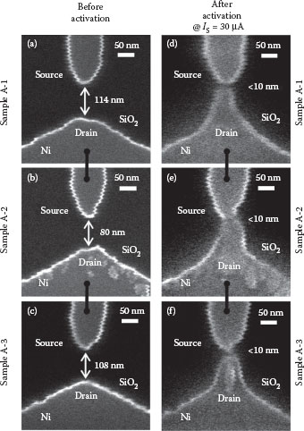
FIGURE 13.2 SEM images of three series-connected Ni nanogaps before (samples (a) A-1, (b) A-2, and (c) A-3) and after (samples (d) A-1, (e) A-2, and (f) A-3) performing the activation with the final preset current IS = 30 μA.
Furthermore, Figure 13.4a shows the drain current ID as a function of the duration of activation TP in the total activation steps with the preset current IS ranging from 1 nA (1st) to 30 μA (8th). The drain current ID is seen to increase exponentially, while increasing the duration of each activation step, as shown in Figure 13.4a. Figure 13.4b also exhibits the relation between the resistance RD, given by VD/ID, and the duration of activation TP with the preset current IS ranging from 1 nA (1st) to 30 μA (8th). It is observed that RD slightly increases at the initial stage of each activation step as the duration of activation TP increases. On the other hand, the value of the maximum resistance RD in each activation step decreases with the progress of activation. This marked decrease in the resistance RD suggests that the formation of a hillock by the accumulation of Ni atoms is caused at the tip of the drain electrode, and then the gap separation is further reduced during the activation with each preset current.
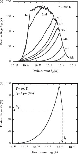
FIGURE 13.3 (a) ID–VD curves of series-connected three samples A-1, A-2, and A-3 during the total activation steps. (b) ID–VD properties of samples A-1, A-2, and A-3 during the 6th activation with the preset current IS = 3 μA. Voltage VS is defined as drain voltage VD at which drain current ID is the same as the preset current IS.
The ID–VD characteristics of each sample after performing the activation with different preset currents IS = 1 nA (1st), 500 nA (4th), and 30 μA (8th) at room temperature are displayed in Figure 13.5. When the preset current IS was set to 1 nA, the ID–VD characteristics showed insulating-like ID–VD properties. On the other hand, the ID–VD curves of the simultaneously activated samples with the preset current IS = 500 nA displayed nonlinear properties. From the figure, although the nanogaps before the activation (or even in the activation with IS = 1 nA) showed insulating properties due to the wide separation of the initial gaps, the nonlinear ID–VD characteristics were obtained after the activation with the preset current IS = 500 nA, which is strongly suggestive of the tunneling properties of the simultaneously activated nanogaps. Additionally, the linear ID–VD properties were also observed when the preset current IS was set to 30 μA. Consequently, the ID–VD properties of the three samples were simultaneously varied from “insulating” to “metallic” through “tunneling” properties by increasing the preset current. These results suggest that the electrical properties of the activated three nanogaps become similar to each other with the progress of the activation, and the accumulation of atoms within the gaps is significantly increased due to the higher preset currents.
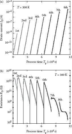
FIGURE 13.4 (a) Drain current ID, passing through samples A-1, A-2, and A-3, as a function of the duration of activation TP in the total activation steps with the preset current IS ranging from 1 nA (1st) to 30 μA (8th). (b) Relation between the resistance RD (= VD/ID) and the duration of activation TP with the preset current ranging from 1 nA (1st) to 30 μA (8th) at room temperature.
Several kinds of nanogap resistances of the samples as a function of the preset current IS during the activation are displayed in Figure 13.6. The tunnel resistances in the low-voltage regime of the three simultaneously activated nanogaps were defined as RA−1, RA−2, and RA−3. The tunnel resistance of each nanogap was individually measured after the activation at room temperature, and decreases simultaneously ranging from 100 TΩ to 100 kΩ while increasing the preset current IS from 1 nA (1st) to 30 μA (8th). This result indicates that the preset current IS is a dominant parameter for simultaneous control of the tunnel resistance of the nanogaps. Moreover, a marked decrease in the tunnel resistance is clearly observed in the range of 100 nA < IS <1 μA. It is interpreted as a transition of the electrical properties of the nanogaps from the insulating regime to the tunneling regime. These results suggest that the wide range of control of the electrical properties of the nanogaps connected in series is achieved by the activation procedure. Additionally, a resistance Rs given by VS/IS and a differential resistance obtained by dVS/dIS were determined during the activation at room temperature and clearly decreased by increasing the preset current IS from 1 nA (1st) to 30 μA (8th), showing a linear relation with a slope of approximately −1. In this figure, the tunnel resistance of the nanogaps after the activation can be successfully predicted by a relation between “RA−1, RA−2, and RA−3 and Rs” or “RA−1, RA−2, and RA−3 and dVS/dIS.” In other words, if we know the RS or the dVS/dIS during the activation procedure, one can easily estimate the tunnel resistance of the nanogaps. This tendency is quite similar to that of individually activated nanogaps [19,20]. Furthermore, it should be noted that the tunnel resistance of simultaneously activated nanogaps was almost the same at each preset current. These results indicate that the simultaneous control of the electrical properties of multiple nanogaps connected in series is successfully achieved by the activation procedure, despite the differences in the samples having different initial nanogap separation distances.
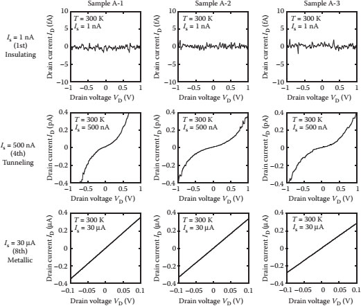
FIGURE 13.5 ID–VD characteristics of samples A-1, A-2, and A-3 after performing the activation with different preset currents IS = 1 nA (1st), 500 nA (4th), and 30 μA (8th) at room temperature.
13.3.2 INTEGRATION OF SETS USING ACTIVATION
The integration method of two SETs based on nanogaps X–1 and X–2 using the activation process is illustrated in Figures 13.7a–e. In the first step, two initial Ni nanogaps with a separation of a few tens of nanometers are fabricated by using conventional EB lithography and lift-off techniques on an SiO2/Si substrate (Figure 13.7a). Next, the F–N field emission current is applied to the initial nanogaps connected in series, as shown in Figure 13.7b. At each nanogap, the migration of Ni atoms from the source (cathode) to the drain (anode) electrode is caused along the direction of the electron flow (Figure 13.7c). The accumulated Ni atoms within the gaps play a dual role of both the reduction of gap width and the formation of islands of SETs. Finally, two SETs are simultaneously integrated using the activation procedure (Figure 13.7d). The advantage of this fabrication method is that the SETs with similar electrical properties could be simultaneously formed because the magnitude of the field emission current becomes the same in each nanogap. Hence, it is strongly suggested that the integration of SETs could be easily achieved by passing a field emission current through many nanogaps connected in series, as shown in Figure 13.7e.
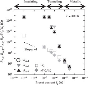
FIGURE 13.6 Dependence of resistances of the nanogaps on preset current IS. The low-bias voltage tunnel resistances RA−1, RA−2, and RA-3, the resistance RS(= VS/IS), and the differential resistance dVS/dIS were estimated from the activation measurements.
Figures 13.8a and b show the SEM images of samples B-1 and B-2, connected in series, before performing the activation, respectively. In these SEM images, initial gap separation of the samples B-1 and B-2 is estimated to be approximately 66 and 50 nm, respectively. Both of the initial nanogaps exhibited high tunnel resistance above 100 TΩ, reflecting the initial gap separation of the nanogap electrodes. On the other hand, the SEM images of both the simultaneously activated samples B-1 and B-2 with the final preset current IS = 10 μA are shown in Figures 13.8c and d, respectively. From the images, the Ni atoms are accumulated in the gap between the source and the drain electrodes at each device, suggesting the formation of the Ni dot/cluster structures (islands) within the gap.
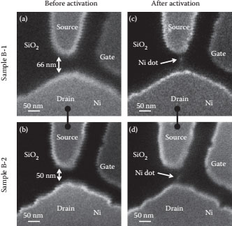
FIGURE 13.8 SEM images of two nanogaps connected in series before (samples (a) B-1 and (b) B-2) and after (samples (c) B-1 and (d) B-2) performing the activation with the final preset current IS = 10 μA.
Figures 13.9a and b represent the ID–VD characteristics of the samples B-1 and B-2, respectively, which are simultaneously activated with the preset current IS = 1.5 μA. For clarity, each ID–VD curve is shifted by 50 fA. In both devices, the gate voltage VG was swept from −14 to 14 V by a 0.5 V step at 16 K. A Coulomb blockade voltage of each device was obviously modulated by the gate voltage VG quasi-periodically. These characteristics suggest that the SETs consist of multiple islands. Modulation properties of the Coulomb blockade voltage (stability diagram) can be more clearly seen in contour plots of the drain current ID of the devices as a function of the drain voltage VD and the gate voltage VG, as shown in Figures 13.9c and d. The charging energy and electrical current levels of both SETs were almost the same. Hence, the two SETs with similar electrical properties were successfully integrated by the activation, despite the difference of initial gap separation between the samples (66 nm in B-1 and 50 nm in B-2). As described above, the preset current during the activation procedure can tune the electrical properties of the devices. In particular, the tunnel resistance of the nanogaps and the charging energy of the SETs show the same tendency on the preset current of the activation in spite of the variation of the initial gap separation of individually activated nanogaps [19, 20 and 21]. In other words, the tunnel resistance and the charging energy of the devices strongly depend on the preset current of the activation but hardly relate to the initial gap separation of the nanogaps [20,21]. Since the two nanogaps are connected in series, the identical field emission current passes through both devices during the activation procedure. Thus, the sample with wider initial gap separation is preferentially and immediately activated by the field emission current with a higher voltage drop. As a result, it is considered that the electrical properties of both SETs become similar to each other with the progress of the activation.
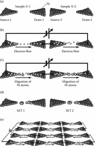
FIGURE 13.7 Sketched description of the integration process using the activation. (a) Two initial nanogaps with separation of a few tens of nanometers are defined by conventional electron beam lithography and lift-off process. (b) Field emission current passes through the two nanogaps connected in series. (c) Ni atoms at the tip of source electrodes, which are activated by the field emission current, are simultaneously migrated from the source (cathode) to the drain (anode). (d) Two SETs are simultaneously formed and integrated by the accumulation of the Ni atoms within the gap. (e) The concept of the large-scale integration of planar-type nanogap-based SETs using the activation procedure.
Figure 13.10 represents the relation between the charging energy EC of the two simultaneously activated SETs and the preset current IS during the activation procedure. Opened circles and triangles indicate the samples B-1 and B-2, respectively. The charging effects of each device were estimated from the Coulomb blockade voltages of the ID–VD curves. As seen in Figure 13.10, the charging energy EC of both simultaneously activated SETs was almost the same at each preset current IS, ranging from 500 nA to 5 μA, where the samples show SET properties. As discussed above, since the preset current IS in the activation procedure is a dominant parameter for controlling the electrical properties of the devices, the integration of the two SETs with similar electrical properties is achieved by passing an identical field emission current through the serially connected nanogaps. Furthermore, as the preset current IS increases from 500 nA to 5 μA, the charging energy EC of both SETs uniformly decreases from approximately 1000 to 150 meV. This tendency is quite similar to that of the individually activated SETs [21]. Therefore, if the activation procedure is applied to the series-connected nanogaps with an appropriate preset current, one can easily obtain the integrated SETs having similar electrical properties. Since the charging energy of the integrated SETs strongly relates to the preset current of the activation, the islands and tunnel barriers placed within the gap between the source and the drain electrodes are simultaneously tuned by the magnitude of the preset current. Hence, it is suggested that the simultaneous control of the charging energy of the integrated SETs is possible with the preset current of the activation. The results imply that the activation method is useful for the integration of nanogap-based SETs with similar electrical properties.
We performed simultaneous tuning of tunnel resistance of multiple nanogaps by a simple and easy method. This method is based on field-emission-induced electromigration and is called “activation.” The control of the tunnel resistance of three nanogaps was simultaneously achieved by performing the activation process for the series-connected nanogaps. The ID−VD properties of the nanogaps were simultaneously varied while increasing the preset current of the activation, indicating that the three nanogaps having similar electrical properties were successfully integrated by the activation process. Furthermore, the tunnel resistance of the simultaneously activated nanogaps decreased, ranging in the order of 100 TΩ to 100 kΩ, while increasing the preset current IS from 1 nA to 30 μA. The gaps of the series combination of the three Ni nanogap electrodes can self-regulate with the final spacing set by the applied current. Consequently, the preset current in the activation procedure can simultaneously tune the tunnel resistance of the integrated nanogaps, in spite of the variation of the initial gap separation of the nanogap electrodes connected in series.
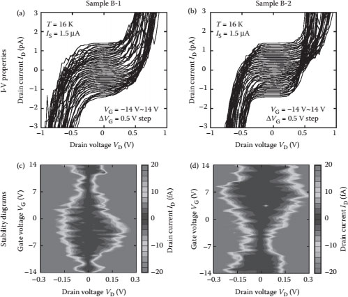
FIGURE 13.9 Current–voltage (ID–VD) characteristics (samples (a) B-1 and (b) B-2) and stability diagrams (samples (c) B-1 and (d) B-2) of two simultaneously activated devices (samples B-1 and B-2) with the preset current IS = 1.5 μA. In ID–VD properties, each curve is shifted by 50 fA for clarity, and gate voltage VG is varied from −14 V (bottom) up to 14 V (top) with a step of 0.5 V.
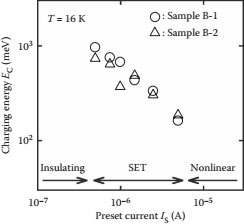
FIGURE 13.10 Charging energy EC of two simultaneously activated SETs (samples B-1 and B-2) as a function of preset current IS at 16 K.
The integration of the SETs was achieved by simultaneously performing the activation procedure for the series-connected nanogaps. The ID–VD curves of the two simultaneously activated devices displayed Coulomb blockade properties. Additionally, the Coulomb blockade voltage of each device was clearly modulated by gate voltage VG. The charging energy and electrical current levels of both SETs were almost the same. As a result, the two SETs with similar electrical properties were successfully integrated by the activation procedure. Moreover, the charging energy of both SETs decreased uniformly with an increase in the preset current. Hence, it is suggested that the simultaneous control of the charging energy of the integrated SETs is possible with the preset current of the activation. These results indicate that the activation procedure is suitable for the simultaneous control of the electrical properties of multiple nanogaps and allows us to integrate planar-type nanogap-based SETs simply and easily.
1. Y. Yasutake, K. Kono, M. Kanehara, T. Teranishi, M. R. Buitelaar, C. G. Smith, and Y. Majima, Simultaneous fabrication of nanogap gold electrodes by electroless gold plating using a common medical liquid, Appl. Phys. Lett., 91, 203107-1-3, 2007.
2. Y. Azuma, Y. Yasutake, K. Kono, M. Kanehara, T. Teranishi, and Y. Majima, Single-electron transistor fabricated by two bottom-up processes of electroless Au plating and chemisorption of Au nanoparticle, Jpn. J. Appl. Phys., 49, 090206-1-3, 2010.
3. D. L. Klein, P. L. McEuen, J. E. B. Katari, R. Roth, and A. P. Alivisatos, An approach to electrical studies of single nanocrystals, Appl. Phys. Lett., 68, 2574–2576, 1996.
4. W. Chen, H. Ahmed, and K. Nakazato, Coulomb blockade at 77 K in nanoscale metallic islands in a lateral nanostructure, Appl. Phys. Lett., 66, 3383–3384, 1995.
5. E. M. Ford and H. Ahmed, Control of Coulomb blockade characteristics with dot size and density in planar metallic multiple tunnel junctions, Appl. Phys. Lett., 75, 421–423, 1999.
6. Y. Nakamura, D. L. Klein, and J. S. Tsai, Al/Al2O3/Al single electron transistors operable up to 30 K utilizing anodization controlled miniaturization enhancement, Appl. Phys. Lett., 68, 275–277, 1996.
7. Y. Nakamura, C. D. Chen, and J. S. Tsai, 100-K operation of Al-based single-electron transistors, Jpn. J. Appl. Phys., 35, L1465–L1467, 1996.
8. J. Shirakashi, K. Matsumoto, N. Miura, and M. Konagai, Room temperature Nb-based single-electron transistors, Jpn. J. Appl. Phys., 37, 1594–1598, 1998.
9. J. Shirakashi, K. Matsumoto, N. Miura, and M. Konagai, Single-electron charging effects in Nb/Nb oxide-based single-electron transistors at room temperature, Appl. Phys. Lett., 72, 1893–1895, 1998.
10. H. Park, A. K. L. Lim, A. P. Alivisatos, J. Park, and P. L. McEuen, Fabrication of metallic electrodes with nanometer separation by electromigration, Appl. Phys. Lett., 75, 301–303, 1999.
11. S. I. Khondaker and Z. Yao, Fabrication of nanometer-spaced electrodes using gold nanoparticles, Appl. Phys. Lett., 81, 4613–4615, 2002.
12. K. Tsukagoshi, E. Watanabe, I. Yagi, and Y. Aoyagi, The formation of nanometer-scale gaps by electrical degradation and their application to C60 transport measurements, Microelectron. Eng., 73, 686–688, 2004.
13. K. I. Bolotin, F. Kuemmeth, A. N. Pasupathy, and D. C. Ralph, Metal-nanoparticle single-electron transistors fabricated using electromigration, Appl. Phys. Lett., 84, 3154–3156, 2004.
14. K. Luo, D.-H. Chae, and Z. Yao, Room-temperature single-electron transistors using alkanedithiols, Nanotechnology, 18, 465203, 2007.
15. D. E. Johnston, D. R. Strachan, and A. T. Charlie Johnson, Parallel fabrication of nanogap electrodes, Nano Letters 7, 2774–2777, 2007.
16. S. L. Johnson, D. P. Hunley, A. Sundararajan, A. T. Charlie Johnson, and D. R. Strachan, High-throughput nanogap formation using single ramp feedback control, IEEE Trans. Nanotechnol., 10, 806–809, 2011.
17. M. Araidai and K. Watanabe, Ab initio calculation of surface atom evaporation in electron field emission, e-J. Surf. Sci. Nanotechnol., 5, 106–109, 2007.
18. P. Kumar and K. Sangeeth, Electric breakdown between nanogap separated platinum electrodes, Nanosci. Nanotechnol. Lett., 1, 194–198, 2009.
19. S. Kayashima, K. Takahashi, M. Motoyama, and J. Shirakashi, Control of tunnel resistance of nanogaps by field-emission-induced electromigration, Jpn. J. Appl. Phys., 46, L907–L909, 2007.
20. Y. Tomoda, K. Takahashi, M. Hanada, W. Kume, and J. Shirakashi, Fabrication of nanogap electrodes by field-emission-induced electromigration, J. Vac. Sci. Technol. B, 27, 813–816, 2009.
21. W. Kume, Y. Tomoda, M. Hanada, and J. Shirakashi, Fabrication of single-electron transistors using field-emission-induced electromigration, J. Nanosci. Nanotechnol., 10, 7239–7243, 2010.
22. S. Ueno, Y. Tomoda, W. Kume, M. Hanada, K. Takiya, and J. Shirakashi, Integration of single-electron transistors using field-emission-induced electromigration, J. Nanosci. Nanotechnol., 11, 6258–6261, 2011.
23. S. Ueno, Y. Tomoda, W. Kume, M. Hanada, K. Takiya, and J. Shirakashi, Field-emission-induced electromigration method for the integration of single-electron transistors, Appl. Surf. Sci., 258, 2153–2156, 2012.