
CONTENTS
14.2 Focused Ion Beam-Based Device Fabrication
Single-electron transistor (SET) devices are of immense interest because of their potential for lowpower operation and high integration density. The basic building blocks of a SET device are tunnel junctions with very small capacitance that are connected in series with a central conducting island. Charge conduction occurs through two tunnel junctions that are connected to the source and drain terminals of the device. As the dimensions of the conducting island reduce to a few nanometers, the electronic wave functions in the conducting island become discrete. The discrete charge on the conducting island is accessed by tunneling through source and drain terminals. The central conducting island is capacitively coupled to a gate terminal, which is used to control the charge on the island. SET devices operate on the principle of a Coulomb blockade, which is the suppression of electron tunneling below a threshold voltage; the capacitance of the tunnel junction system dictates the threshold voltage, whereas a Coulomb blockade is observed when the device dimensions are reduced to a few nanometers [1]. SET devices can be realized with semiconducting or metallic systems. This chapter looks at metallic systems where tungsten and tungsten oxide are used. A pictorial view of a double-junction SET device is shown in Figure 14.1, where the conducting island is sandwiched between the two tunnel junctions that are connected to the source and drain terminals. One tunnel junction is characterized by the tunnel resistance Rt1 and capacitance C1, whereas the other tunnel junction is characterized by the resistance Rt2 and capacitance C2, and the capacitance of the gate coupled to the central conducting island is Cg. The energy required to add an electron to the conducting island is the charging energy, and the external applied bias provides energy for tunneling. If the applied bias is greater than the charging energy, it results in electron tunneling.
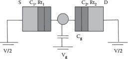
FIGURE 14.1 Pictorial view of the double-junction SET device.
The ambient thermal temperature also provides energy for tunneling; if the charging energy is less than the thermal noise, the Coulomb blockade events are dissipated. For room-temperature operations of SET devices, the charging energy should be greater than the thermal noise. The Coulomb blockade events are observable at room temperature if discrete energy levels can be maintained in the central conducting island; the high tunnel resistance of the tunnel junctions helps to confine the electronic wave function and results in the room-temperature operation of these devices. There are two important constraints on SET device operations: the capacitance associated with the central island should be very small and the tunnel junction resistance should be very large [2]. For the room-temperature operation of SET devices, the confinement of electrons to the central conducting island is a necessary requirement. For the room-temperature operation of SET devices, the conducting island dimensions should be below 10 nm for the capacitance to be favorable. Technologically, the fabrication of sub-10 nm features is a challenge. Many approaches have been used in the past for the realization of SET devices; we present the fabrication of SET devices based on focused ion beam (FIB) techniques. This work looks at a multijunction SET system with tungsten as a conducting island and tungsten oxide as a tunnel junction. An FIB system is used for the fabrication of a SET device, and both FIB etching and deposition have been investigated. The fabricated multijunction SET devices show a room-temperature Coulomb blockade. The key to the realization of room-temperature-operating SET devices is the fabrication of sub-10 nm nanoparticles in tungsten using FIB deposition and the chemical oxidation of tungsten in peracetic acid to realize high-resistive tunnel junctions. Based on the oxide thickness of the tungsten oxide, the barrier height of the fabricated tunnel junctions were in the range of ~1.5–2.5 eV. The device characteristics for the multijunction SET system are presented showing a clear Coulomb blockade with the charging energies close to 160.0 meV. The SET device is a very sensitive electrometer; the charge on the gate electrode of the SET device can be used to modulate the device characteristics; thus, the SET device can be used as a sensor. The charge on the gate electrode can be modulated using a chemical, optical, electrical, or any other transduction mechanism. The current work looks at a SET device as a gas sensor.
14.2 FOCUSED ION BEAM-BASED DEVICE FABRICATION
FIB technologies have been very useful in the realization of nanostructures for nanoelectron devices [3,4]. An FIB system is very similar to a scanning electron microscope (SEM) in operation but uses a focused beam of Ga+ ions. It was used in this work for the selective modification of the sample surface. FIB systems can be used for etching and deposition; both the techniques have been investigated for SET device fabrication. FIB etching resulted in a minimum island size of 40 nm. Conducting islands below 40 nm were not feasible to be fabricated using FIB etching, and the interaction of beam energies during FIB etching for islands below 40 nm resulted in the evaporation of the island’s material being etched as shown in Figure 14.2 [5]. FIB deposition uses a precursor gas that is chemically adsorbed on the sample surface, and the energy for the chemical reaction is provided by the FIB beam energy, resulting in the desired material being deposited on the sample surface and the other gases, the by-products, being removed by the FIB vacuum system. FIB deposition was used for the successful deposition of nanoislands of sub-10 nm dimensions for the realization of the SET devices.
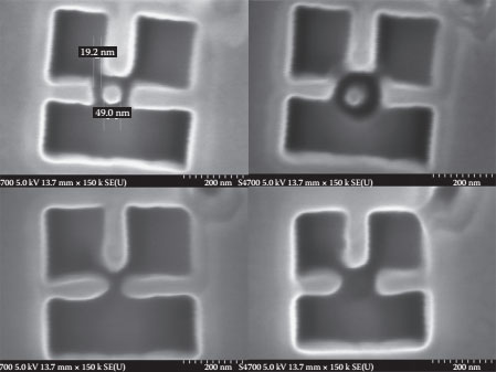
FIGURE 14.2 Minimum island size with FIB etching.
A silicon substrate having a 300 nm-thick A12O3 passivating film deposited using a Perkin-Elmer 2400-8J parallel plate radio frequency (rf) sputtering system was used. Nanoislands were randomly deposited on the sample surface. The tungsten nanoislands were fabricated using FIB deposition in a Hitachi FB-2000A system [6]. The nanoislands were deposited randomly in an area of 16 μm × 16 μm on an A12O3 thin film. The average diameter of the tungsten nanoislands was 8 nm with an average height of 3.3 nm. To reduce the size of the islands further, the sample was subjected to a brief chemical etch in a 1:1 sulfuric peroxide solution (piranha etch). The samples were rinsed in deionized water and then introduced into a solution of peracetic acid, which is a mixture of glacial acetic acid and hydrogen peroxide in a 1:1 volume ratio. Peracetic acid, being a strong oxidizing agent, was considered for the oxidation of tungsten. A pictorial view of the deposited nanoislands and the chemically oxidized tungsten islands is shown in Figure 14.3.
Thermal oxidation of tungsten nanoislands was considered but the higher temperatures involved in the thermal oxidation of the tungsten nanoislands were found to increase the nanoisland size, thus degrading the room-temperature performance of the SET device. The initial oxidation of tungsten nanoislands was performed by thermal oxidation; the high temperature of ~900°C in the process led to an increase in the island size. An increase in the island size is not desirable for room-temperature operation of a SET device; the capacitance of the SET device increases with an increase in the island size. The oxidation of tungsten nanoislands needs to be performed at lower temperatures, which help retain a lower island size. The chemical oxidation of tungsten using peracetic acid was the best alternative in maintaining the critical dimensions of the tungsten nanoislands to realize the room-temperature operation of the SET devices. The fabricated tunnel islands and the comparison of tungsten oxide between thermal and chemical oxidation can be seen in Figure 14.4.
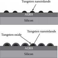
FIGURE 14.3 Pictorial view of the fabricated tungsten nanoislands and the chemically oxidized tungsten nanoislands forming tungsten oxide tunnel junctions. (P. S. K. Karre et al., High resistive tunnel junctions for the room temperature operating single-electron transistor fabricated using chemical oxidation of tungsten nano particles, Digest IEEE Int’l Conference on Nanotechnology (Nano 2011), August 13–18, Portland, OR, pp. 1456–1459, © (2011) IEEE. With permission.)
Tungsten oxide acts as tunnel junctions for the device. The connecting nanowires from the source, drain, and gate terminals were also fabricated using FIB deposition, and after the formation of tunnel junctions, the nanowires were deposited in tungsten connecting the active area of the device to the source, drain, and gate terminals. To estimate the thickness of tungsten oxide formed around the tungsten nanoislands during the chemical oxidation process, a cross section of the sample was polished using electromechanical polishing down to 1 μm smoothness. The nanoislands were deposited close to the edge of the polished wafer surface. The oxidation time of the as-deposited tungsten nanoislands was varied from 1 to 30 min. The samples of tungsten nanoislands deposited using FIB deposition were introduced into peracetic acid after a quick dip in piranha solution and then oxidized in peracetic acid for different time intervals from 1 to 30 min. The samples were rinsed in deionized water and dried in a nitrogen ambient. The cross section of the sample was milled using FIB etching and observed using a field emission scanning electron microscope (FE-SEM) to estimate the thickness of the tungsten oxide. A cross section of one of the samples is shown in the SEM micrograph in Figure 14.5, showing the FIB milled cross section of the sample with tungsten nanoislands and the deposited tungsten oxide in the series of SEM micrographs.
The SEM micrograph in Figure 14.6 shows the source, drain, and gate terminals of the fabricated multijunction SET device. The dimensions of the source drain and gate terminals are 100 × 100 μm2 and the connecting leads are 50 μm in length and 250 nm in width. All the connecting nanostructures for the device are fabricated using FIB deposition of tungsten. The deposition parameters were different for the connecting nanoleads, nanoislands and the source, drain, and gate terminals with different beam currents, and beam apertures to realize the differences in the nanostructures in the as-deposited films. The conducting nanoislands of tungsten were deposited in an area of 16 μm × 16 μm on the Al2O3 thin film at the center of the device with a beam having a beam current of 2.0–3.5 nA as shown in the exploded view of the SEM micrograph. The nanoislands are randomly deposited between the source and drain terminals. The geometry of the device allows 10 nanoislands between the source and drain terminals along the source and drain terminals, thus making the device a multijunction SET system. The average height of the deposited nanoislands is 3.3 nm as shown in the atomic force microscopy (AFM) micrograph of the as-deposited nanoislands of tungsten using FIB deposition. The nanoislands were deposited last after the deposition of probing pads and the connecting nanoleads of the device. The fabricated SET structure was oxidized in peracetic acid to form the tungsten oxide; the tungsten oxide was formed on top of the nanoislands, reducing the height and size of the as-deposited tungsten nanoislands as well as the entire device. A blanket thin film of 30 nm Al2O3 was deposited as a passivating layer on top of the fabricated SET device; FIB etching was used to open up the underlying source, drain, and gate terminals by timed FIB etching of the passivating Al2O3 layer using a beam having a beam current of 4.0–8.0 nA for an etch time of 10 min. The AFM micrograph shows the nanostructure of the as-deposited tungsten nanoislands using FIB deposition in Figure 14.6. The SET device fabrication with the FIB deposition process is a slow process, and to demonstrate a progression toward large-scale production of these devices, step and flash imprint lithography (SFIL) was successfully utilized for the fabrication of the connecting nanowires from the source, drain, and gate terminals coming into the active area of the device. The active area of the device is fabricated using FIB deposition of the nanoislands in tungsten. The fabricated SET devices using SFIL and FIB deposition show clear Coulomb blockade properties at room temperature. The micrograph in Figure 14.7 clearly shows the SFIL fabricated structures with the SET devices [8].
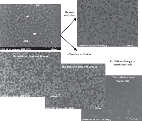
FIGURE 14.4 Oxidation of tungsten nanoislands using chemical oxidation in peracetic acid. (P. S. K. Karre et al., High resistive tunnel junctions for theroom temperature operating single-electron transistor fabricated using chemical oxidation of tungsten nano particles, Digest IEEE Int’l Conference on Nanotechnology (Nano 2011), August 13–18, Portland, OR, pp. 1456–1459, © (2011) IEEE. With permission.)
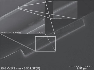
FIGURE 14.5 Cross section of one of the samples showing the tungsten nanoislands and the tungsten oxide formed after the chemical oxidation in peracetic acid. (P. S. K. Karre et al., High resistive tunnel junctions for theroom temperature operating single-electron transistor fabricated using chemical oxidation of tungsten nano particles, Digest IEEE Int’l Conference on Nanotechnology (Nano 2011), August 13–18, Portland, OR, pp. 1456–1459, © (2011) IEEE. With permission.)
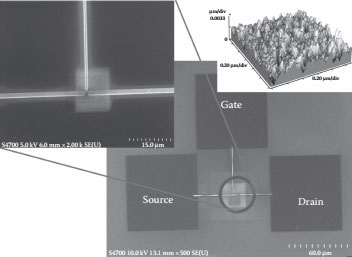
FIGURE 14.6 SEM micrograph of the fabricated STE device, active area, and the as-deposited tungsten nanoislands. (P. S. K. Karre et al., High resistive tunnel junctions for theroom temperature operating single-electron transistor fabricated using chemical oxidation of tungsten nano particles, Digest IEEE Int’l Conference on Nanotechnology (Nano 2011), August 13–18, Portland, OR, pp. 1456–1459, © (2011) IEEE. With permission.)
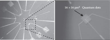
FIGURE 14.7 Micrograph showing the SFIL and FIB deposited SET devices.
The tungsten oxide thickness for different oxidation times was estimated using the FE-SEM measurements from a cross section of the sample. The EDS and AFM methods were also used to characterize the tungsten oxide thin films. The thickness of the tungsten oxide increased from 2.3 nm for a 60 s oxidation to 9.6 nm for an oxidation time of 360 s and decreased thereafter. The thickness of the tungsten oxide increased with the oxidation time initially; as the tungsten became more hydrated and soluble, it was found to dissolve in the hydrogen peroxide present in the peracetic acid [9,10], thus reducing the thickness of the tungsten oxide and the tungsten after 360 s. The tungsten nanoislands were completely oxidized and dissolved for an oxidation time of 20 min and more. All the samples that were oxidized had a starting average island size of ~8 nm.
The tungsten oxide tunnel junctions were characterized by fabricating the SET devices and extracting the junction parameters from the device characteristics. The device characteristics of the room-temperature-operating SET device were obtained using the Keithley 4200-SCS semiconductor characterization system coupled with a Micromanipulator 8000 series probe station. The device characteristics showed a clear Coulomb blockade and Coulomb oscillations in the differential conductance of the device as shown in Figure 14.8. The characteristics for the two different devices are shown where the source and drain characteristics for different gate voltages are investigated. The measurements were performed at a room temperature of 23°C. The source drain voltage of the device was varied from −3.0 to 3.0 V for a fixed gate voltage of 33.0 mV and 1.6 V. The drain current of the SET device was found to be of the order of a few pA, showing a clear Coulomb blockade and Coulomb oscillations in the differential conductance of the device; the single-electron effects were observed in multiple devices showing that the SET device characteristics were reproducible across multiple devices. The drain current shows a variation in the blockade voltage based on an applied gate bias. A fine structure in the nonlinear device characteristics was seen at higher source and drain voltages due to the differences in the actual island size of the individual conducting islands and the oxide thickness resulting from these variations, thus making the tunnel junctions asymmetrical in nature.
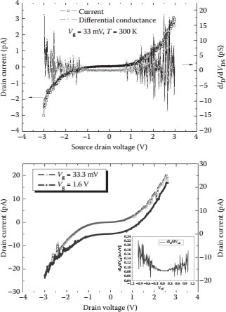
FIGURE 14.8 The I–V characteristics of a working SET device at room temperature showing a clear Coulomb blockade for different gate voltages. (P. S. K. Karre et al., High resistive tunnel junctions for theroom temperature operating single-electron transistor fabricated using chemical oxidation of tungsten nano particles, Digest IEEE Int’l Conference on Nanotechnology (Nano 2011), August 13–18, Portland, OR, pp. 1456–1459, © (2011) IEEE. With permission.)
It is estimated from the geometry of the device that there are 10 nanoislands participating in the conduction process, thus making the device a 20-junction SET system. Assuming that all the tunnel junctions are similar and have the same capacitance and resistance, the charging energy of the device can be calculated using the Orthodox theory [11,12] that is applied to a multijunction SET system. The device parameters were extracted from the (I–V) characteristics of the device, and the resistance of the tunnel junctions was found to be ~29 GΩ, which is much larger than the quantum of resistance (~26 KΩ). The effective capacitance of the device was found to be 0.499 aF. The capacitance of the individual junction was estimated to be 0.947 aF, and the charging energy of the device was found to be 160.0 meV. The threshold voltage of the device was estimated on the basis of the effective capacitance of the device ~0.4 V, but the actual threshold voltage of the device can be seen to be ~0.7–1.5 V. This difference in the threshold voltage is due to the fact that all the conducting islands are nonuniform and contribute to the differences in the actual threshold voltage and the estimated threshold voltage, where all the junctions were considered to be identical for the device parameter extraction. The barrier height of the tunnel junctions was extracted from the conductance of the device by using the Brinkmann fit method [13]. The barrier height of the tunnel junctions was found to vary from ~2.3 to ~1.3 eV for thicknesses of ~2 to ~9 nm, respectively.
The SET device has been demonstrated to be an N2O gas sensor, where the sensing mechanism is based on the charge modulation on the gate electrode due to the interaction of the incoming gas species with the surface complexes on the gate electrode. The gas sensing is expected to be mediated through ionosorption [14] of the gas molecules on the surface of the gate terminal. Figure 14.9 shows the proposed sensing mechanism of the SET gas sensor, where the incoming gas molecules are adsorbed on the gate surface, facilitating charge transfer [15].
The gate terminal is made of tungsten using the FIB deposition process. The nonlinear Coulomb blockade along with the Coulomb oscillations are shown in Figure 14.10; the blockade length (the voltage range where the current is not increasing) of the device was ~6.0 V without the introduction of N2 gas into the chamber. With the N2 gas in the chamber, the blockade length reduced to ~2.0 V. The reduction in the blockade length of the device is attributed to the increase in the overall capacitance of the device due to the adsorption of the gas molecules on the gate surface. The drain current of the device was monitored as a steady stream of N2 gas was injected into the flow cell; after the injection of the steady stream of N2 gas, a constant flow of N2O gas was injected, which reduced the drain current of the device. The presence of the incoming gas molecules can be sensed by the reduction of the drain current of the device and also by the reduction of the Coulomb blockade length of the device. The sensing mechanism was through ionosorption; the native amorphous tungsten oxide surface of the gate pad has an interatomic distance of 1.79 Å between tungsten and oxygen [16]. The number of available tungsten oxide sites for the ionosorption of the incoming gas on a 100 μm × 100 μm pad was calculated to be approximately 7.8 × 10¹⁰. The stable isotopic configuration expected for N2O is N–N–O [17], and the number of electrons transferred between N2O and the WO3 surface was calculated to be approximately 1.56 × 10¹¹, which is in close agreement with the measured drop in the drain current. Depending on the surface state of the gate terminal and the incoming gas molecule, the electrons can be transferred to or from the gate terminal. The removal of electrons from the gate terminal induces a positive bias on the gate, resulting in a downward spike in the drain current, and vice versa. The SET device characteristics are modulated on the basis of the charge transfer on the gate terminal. The SET device has also been demonstrated to be a photondetector using bacteriorhodopsin [18].
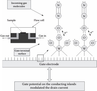
FIGURE 14.9 Proposed ionosorption mechanisms resulting in charge transfer in the SET device.
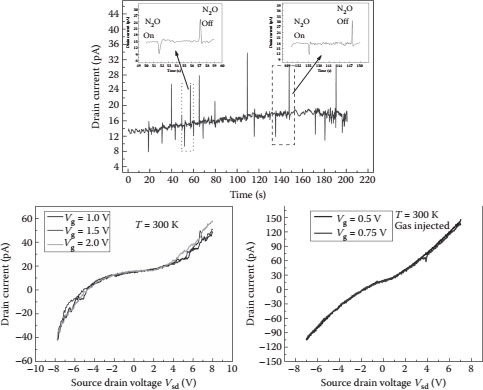
FIGURE 14.10 Coulomb blockade changes with and without gas injection.
A novel approach was developed in the fabrication of high-resistive tunnel junctions for room-temperature-operating SETs using the chemical oxidation of tungsten nanoislands in peracetic acid. The tunnel junction thickness was found to increase and then decrease due to the dissolution of tungsten in peracetic acid with increased dissolution times. The tunnel junctions were estimated to have a tunnel resistance of ~29 GΩ; the SET devices fabricated with these large tunnel-resistant tunnel junctions showed a clear Coulomb blockade and Coulomb oscillations at room temperature. The fabricated tunnel junctions had an estimated barrier height in the range of ~2.3 to ~1.3 eV for thicknesses of ~2 to ~9 nm, respectively. The effective capacitance of the device was found to be 0.499 aF. The capacitance of the individual junction was estimated to be 0.947 aF, and the charging energy of the device was found to be 160.0 meV. The SET device was used as a gas sensor demonstrating the sensing of N2O gas with the SET device and an optical sensor using bacteriorhodopsin.
The research reported in this document was performed in connection with contract DAAD17-03-C-0115 with the U.S. Army Research Laboratory.
1. H. Grabert and M. H. Devaret, Single Charge Tunneling, Coulomb Blockade Phenomena in Nanostructures, Plenum, New York, 1992.
2. K. K. Likharev, Single-electron devices and their applications, Proc. IEEE 87, 606, 1999.
3. D. Petit aid, D. Wood, R. P. Cowburn, C. C. Faulkner, and S. Johnstone, Nanometer scale patterning using focused ion beam milling, Rev. Sci. Instr., 76, 026105, 2005.
4. M. Nakayama, F. Wakaya, J. Yanagisawa, and K. Gamo, Focused ion beam etching of resist/Ni multilayer films and applications to metal island structure formation, Journal of Vacuum Science & Technology B: Microelectronics and Nanometer Structures, 16(4), 2511, 2514, Jul 1998. doi: 10.1116/1.590200.
5. P. S. K. Karre, P. L. Bergstrom, G. Mallick, and S. P. Karna, Fabrication of quantum islands for single electron transistors using focused ion beam technology, Proc. IWPSD’05: Thirteenth Int. Workshop on the Physics of Semiconductor Devices, 2005.
6. P. S. K. Karre, P. L. Bergstrom, G. Mallick, and S. P. Karna, Room temperature operational single electron transistor fabricated by focused ion beam deposition, J. Appl. Phys., 102, 024316, 2007.
7. P. S. K. Karre, D. D. Cheam, M. Acharya, and P. L. Bergstrom. High resistive tunnel junctions for theroom temperature operating single electron transistor fabricated using chemical oxidation oftungsten nano particles, Digest IEEE Int’l Conference on Nanotechnology (Nano 2011), 13–18 August 2011, Portland, OR, pp. 1456–1459.
8. D. D. Cheam, P. S. K. Karre, M. Palard, and P. L. Bergstrom, Step and flash imprint lithography for quantum dots based room temperature single electron transistor fabrication, Microelectron. Eng., 86(4–6), 646–649, 2009.
9. G. S. Kanner and D. P. Butt, Raman and electrochemical probes of the dissolution kinetics of tungsten in hydrogen peroxide, J. Phys. Chem. B, 102, 9501, 1998.
10. B. Reichman and A. J. Bard, The electrochromic process at WO3 electrodes prepared by vacuum evaporation and anodic oxidation of W, J. Electrochem. Soc., 126, 583, 1979.
11. J. P. Pekola, K. P. Hirvi, J. P. Kauppinen, and M. A. Paalanen, Thermometry by arrays of tunnel junctions, Phys. Rev. Lett., 73, 2903, 1994.
12. K. P. Hirvi, J. P. Kauppinen, A. N. Korotkov, M. A. Paalanen, and J. P. Pekola, Arrays of normal metal tunnel junctions in weak Coulomb blockade regime, Appl. Phys. Lett., 67, 2096, 1995.
13. W. F. Brinkman, R. C. Dynes, and J. M. Rowell, Tunneling conductance of asymmetrical barriers, J. Appl. Phys., 41(5), 1970.
14. M. J. Madou and S. R. Morrison, Chemical Sensing with Solid State Devices, Academic Press Inc, Boston, MA, 1989.
15. P. S. K. Karre, M. Acharya, W. R. Knudsen, and P. L. Bergstrom, Single electron transistor based gas sensing with tungsten nano particles at room temperature, IEEE Sensors J., 8(6), 797–802, 2008.
16. F. Wang and R. D. Harcourt, Electronic structure study of the N2O isomers using post-Hartree-Fock and density functional theory calculations, J. Phys. Chem. A. (Article) 104(6), 1304–1310, 2000.
17. T. Pauporte, Y. Soldo-Olivier, and R. Faure, XAS study of amorphous WO3 formation from a peroxotungstate solution, J. Phys. Chem. B. (Article) 107(34), 8861–8867, 2003.
18. K. A. Walczak, M. Acharya. D. Lueking, P. L. Bergstrom, and C. Friedrich, Integration of the bionanomaterial bacteriorhodopsin and single electron transistors, Proceedings of the 26th Army Science Conference, Paper #MP-06, December 2008, Orlando, FL, USA. 4 p.