
CONTENTS
15.3 Optimal Arrays for Minimizing Power
15.4 Axon-Inspired Communication in Single Electron Technology
The latest ITRS (International Technology Roadmap for Semiconductors) [1] has identified power consumption as a grand challenge for nanoelectronics. A related daunting task is represented by the passive wires (interconnects), see [2, 4, 5, 6, 7 and 8]. They are the ones driving the power/energy consumption, as their number increases exponentially (each device has to be connected by several wires to other devices, and the number of devices is following the exponential Moore’s law), while their scaling is limited (as their parasitic capacitances and RC-delays are not scaling in sync with the devices). In fact, the huge processing potential offered by parallel architectures will not be realized satisfactorily without addressing the interconnection challenge which is intimately entangled with power and energy consumption. During the 2011 International Solid-State Circuits Conference, power consumption has been a leitmotif [9]. Dr. Oh-Hyun Kwon, the president of Samsung Electronics, has stated the need “to reduce power consumption by a compound annual rate of 20% over the next decade,” while Professor Asad Abidi (University of California, Los Angeles) has mentioned that the power efficiency challenge “requires radical changes in the way we do things.” One of the radical approaches—advocated by Dr. Jack Sun, Vice President for Research and Development and Chief Technology Officer of TSMC, to solve the challenges associated with power constraints—the chip industry could envisage is to “get some inspiration from the amazing human brain.” On the one hand, structures in the brain are characterized by massive interconnections, but, contrary to common thought, most of these are local with an amazingly sparse global interconnect network. On the other hand, cortical neurons possess an average of 8000 (up to a maximum of 100,000) synaptic connections, which differentiate them significantly from present-day CMOS (complementary metal–oxide–semiconductor) gates having an average of four inputs only. With on the order of 1010 neurons in the human cortex, and about 1014 synaptic connections, the brain is inspirational for the future of interconnects (supporting massively parallel multi-/many-cores) due to its ultra-low-power consumption (about 20 W) and extreme reliability. This is because the neurons themselves are able to communicate (dendritic and axonal communications) at quite large distances on a very limited power budget.
If we consider an older 1.0 μm technology (using an Al and SiO2 dielectric), the transistor delay was 20 ps, and the RC delay of a 1 mm line was 1 ps. In a 32 nm technology (using Cu and low-k dielectric), the transistor delay is about 1 ps, and the RC delay of a 1 mm line is around 250 ps. In addition, up to 80% of microprocessor power is being consumed (wasted) by interconnects [10]. This communication challenge [11] is only now starting to be fully appreciated as it is bridging the power and the reliability challenges, as on-chip communications are getting more and more power hungry and less and less reliable (i.e., more and more sensitive to noise and variations). Just like the wires connecting the devices inside an integrated chip, the connections between neurons occupy a large fraction of the total volume, and the “wires” (dendrites and axons) consume energy during signaling. In fact, although the human brain represents only 2% of the total body weight, it consumes 20% (going up to 40% for kids) of its resting energy. Impressive advances in brain scanning have evolved from the early positron emission tomography—PET (developed about 20 years ago), to magnetic resonance imaging—MRI (developed about 10 years ago). Variations include functional MRI (fMRI), blood oxygen level-dependent (BOLD) MRI, and diffusion MRI among others. These have led to a very precise mapping of the brain’s functional areas and of their connectivities (see Figure 15.1). The rapidly developing diffusion tensor MRI (DT-MRI) offers the means of probing the structural arrangement of tissue at the cellular level, and has already been used to estimate the brain connectivity. Such techniques can be used to map the path of (white matter) tracts in the brain in vivo noninvasively, using the so-called tractography methods.
All of these results are supporting the scarcity of the long interconnects in the brain. The detailed map of the full set of neurons and synapses within the nervous system of an organism is known as a connectome (http://en.wikipedia.org/wiki/Connectome), and the National Institutes of Health is supporting the Human Connectome Project (http://www.humanconnectomeproject.org/), which started in 2011. In fact, the first comprehensive attempt to reverse-engineer the mammalian brain was started in 2005 as the EPFL/Blue Brain Project (http://bluebrain.epfl.ch/), and impressive simulation results of neocortical columns (about 10,000 biologically accurate individual neurons) have already been obtained (see Figure 15.2). The expectation is that the Blue Brain Project will be expanded and continued under the EU’s FET Flagship program as the Human Brain Project (http://www.humanbrainproject.eu/), a fact which has just been announced in January 2013 (http://www.nature.com/news/brain-simulation-and-graphene-projects-win-billion-euro-competition-1.12291).
Transferring information inside the brain is in fact achieved by both electrical and chemical processes. Inside one neuron (see Figure 15.3a), information is transmitted along the dendrites and axons by electrical pulses supported by the active membrane—and in particular by the voltage-gated ion channels. The gaps between neurons are known as synaptic clefts, and represent obstacles for these pulses. Chemicals called neurotransmitters are used to convey information over these gaps.
Neurons themselves are isolated by semipermeable membranes which act as barriers to particular types of ions. The movement of ions through a membrane is controlled by many different ion channels. It is this movement that leads to different ion concentrations inside and outside a neuron, which in turn creates a difference of potential called membrane potential. Normally, the concentration of Na+ is higher outside a neuron, while the concentration of K+ is higher inside the neuron. Besides ion channels, which are normally closed most of the time and open only very briefly, the Na+/K+ pumps are the ones responsible for maintaining these ion concentrations.
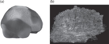
FIGURE 15.1 The brain: (a) Tensor visualization with MedINRIA (from http://www-sop.inria.fr/asclepios/software/MedINRIA/screenshoots/); (b) HARDI (high angular resolution diffusion imaging) tracks showing information transfer between the two hemispheres (from http://www.humanconnectomeproject.org/wp-content/uploads/2011/06/cing7-e1307569111895-720x476.jpg).
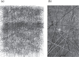
FIGURE 15.2 A cortical column: (a) Layers and their connectivity; (b) Simulated view inside a cortical column. (©BBP/EPFL, from http://bluebrain.epfl.ch/) (©BBP/EPFL, from http://bluebrain.epfl.ch/)
Trying to find inspiration from the neurons in general, and from the way they communicate in particular, this chapter will focus on the axon-inspired communication (i.e., at long distances and on a limited power budget), analyzing the dense and locally connected arrays of voltage-gated (nonlinear) ion channels [12, 13, 14 and 15]. The resulting arrays of the voltage-gated ion channels will be simulated at the logical level using single-electron technology/transistors (SETs) [16]. Such an approach should lead to practical power/energy lower bounds for nanoelectronics.
In the early 1950s, scientists were starting to understand the propagation of the action potential as the basis for the propagation of nerve impulses [12,13]. That theory became a cornerstone of cellular biophysics, and set an entire field of scientists to work on excitable membranes. Inside one neuron (Figure 15.3a), information is transmitted by electrical pulses [17] along the dendrites and axons. The pulses are shaped and propagated by the active membrane, which contains many voltage-gated ion channels. Ion channels are pore-forming proteins (or an assembly of several proteins) [18] which are present in the membranes (lipid bilayers) of all biological cells [19,20]. The typical ion channel is about one or two atoms wide and it is both very selective (ion specificity being about 1/10,000) as well as fast (allowing the passage of about 107–8 ions/s). Ions like, for example, Na+ and K+ can move across the cell membrane based on their gradients. The ions move through an ion channel in a row [21,22] conceptually similar to, but physically very different from, the tunneling events of single-electron transistors [23]. Some ion channels are controlled by a “gate” which may open or close selectively, performing exactly like a switch. In particular, voltage-gated ion channels open or close depending on the voltage gradient across the membrane [24,25], and behave very similarly to the well-known transistors. In a recursive manner, these voltage-gated ion channels allow the flow of certain (selected) ions down their electrochemical gradient, and hence they are themselves creating, maintaining, and propagating the voltage gradients across the membrane.
When a neuron is stimulated, the voltage-gated Na+ channels open and the Na+ ions start flowing into the cell. This causes a local increase of the membrane potential, which in turn activates neighboring voltage-gated Na+ channels, which also open. The resulting local depolarization also stimulates nearby voltage-gated K+ channels to also open. Therefore, K+ ions start flowing out of the cell in a process called repolarization. Still, even before the Na+ and K+ ions across the membrane equilibrate, both the Na+ and K+ channels close automatically after a very brief period of time (resting). The main result of these timely orchestrated actions of large numbers of voltage-gated ion channels is a local and moving reversal of the membrane potential, which is known as an action potential (Figure 15.3b). In the end, K+ ions move outside and restore the resting potential. The resulting “spikes” are the ones representing and propagating information along an axon. After an action potential has taken place, there is a period of time (known as the refractory period) during which the membrane cannot be stimulated again.
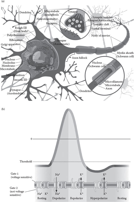
FIGURE 15.3 (a) A myelinated neuron (from http://en.wikipedia.org/wiki/File:Complete_neuron_cell_diagram_en.svg); (b) Action potential (theoretical approximation of the membrane potential). (From http://www.mhhe.com/biosci/esp/2001_gbio/folder_structure/an/m2/s4/assets/images/anm2s4_1.jpg.)
A detailed understanding of the energy consumption associated with an action potential is still in its infancy, but it is a hot topic very actively pursued. For details, the interested reader should consult Refs. [27, 28, 29, 30, 31, 32, 33, 34, 35, 36, 37, 38, 39, 40, 41, 42 and 43]. In this chapter, we are not going to analyze such aspects; our aim is to show how borrowing some inspiration from the way axons communicate could be translated to another implementation medium—nanoelectronics.
15.3 OPTIMAL ARRAYS FOR MINIMIZING POWER
Obviously, as our major aim is to reduce power, it seems only normal that we would want to minimize the number of ion channels. It follows that the neighboring ion channels (i.e., the ion channels around a given ion channel) should be positioned in some optimal way. This can be better appreciated by looking at Figure 15.4a, which—although not an array of ion channels—endorses nature’s appetite for arrays at the nanoscale. Additionally, one would also want to reduce the time the ion channels are open while also maximizing the distances they can communicate (also known as broadcast coverage area), but unfortunately these two aims are conflicting.
Here, we present an upper bound on the broadcast coverage area with the condition that each voltage-gated ion channel (which is in fact both “a sensor” and “a broadcasting node”) is assumed to be surrounded by the same number of neighboring voltage-gated ion channels (which means that here we consider only regular arrays). All the voltage-gated ion channels are used just for rebroadcasting the information, that is, for propagating the action potential further. This interpretation of the membrane of an axon is equivalent to a sensor network used for broadcasting a message. That is why it can be modeled using the unit disk graph [44]. Each and every voltage-gated ion channels will be considered to communicate/broadcast over a disk of radius r (which is related to the time the voltage-gated ion channel is open). As shown in Figure 15.4b, X is defined as the originating node (there is normally more than one originating node). X broadcasts information to its neighboring ion channels Yi, located inside a circle as |XYi| ≤ r, for further rebroadcasting. Let TAk,n be the total broadcast coverage area of m(k,n) ion channels as in a k-hop broadcasting scheme, and ASk,n be the broadcast coverage area of each ion channel involved in this broadcasting process. Here, k represents the number of broadcasting hops from ion channel X, while n is the number of neighboring ion channels.
We consider simplistically that information (i.e., the flow of ions) from X travels in a “single hop” to the neighboring ion channels Yi (i = 1, 2, …, n). The total “coverage area” will be determined by the distance |XYi| and the forwarding angles αi = ∠YiXYj, where j = (i + 1) mod n.
Theorem: If an ion channel X has n (n ≥ 3) neighboring ion channels Yi (i = 1, 2, …, n) for broadcasting relay, the total broadcasting coverage area is optimized when all forwarding neighboring ion channels Yi are symmetrically located on the border of X’s transmission range.
Proof: The total broadcasting coverage area TA1,1(x) is given by
(15.1) |
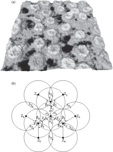
FIGURE 15.4 (a) Nuclear envelope of Xenopus laevis oocyte, a “biological nano-array,” imaged with atomic force microscopy (area is about 600 nm × 600 nm; from http://celldynamics.uni-muenster.de/Projects/ProA6txt.html); (b) multi-hop broadcast with three forwarding neighboring nodes (i.e., three voltage-gated ion channels surrounding each voltage-gated ion channel).
where x is the distance between X and Yi. Differentiating, we obtain:
(15.2) |
It follows that TA1,1(x) is maximized when x = r:
(15.3) |
Hence, when xi = r = 1, the total broadcast coverage area is:
(15.4) |
with and αi the angle between X and Yi (as defined above), while SVi is the overlapping area between two adjacent ion channels. When αi ≥ 2 π/3, SVi(αi) = 0. From Equation 15.4, we can infer that TA1,n is maximized when is minimized. Using Lagrange relaxation, let
(15.5) |
Define:
(15.6) |
with β the Lagrange multiplier. F is minimized if:
(15.7) |
Hence:
The solution for Equation 15.7 is αi = 2 π/n (i = 1,2,…n); therefore, Max(TA1,n) can be obtained if and only if:
This implies that TA1,n is maximized when Yi are symmetrically located on the border of X’s transmission range.
As an example, let us consider a single-hop broadcast relay scheme from X via three neighboring ion channels Yi (i = 1, 2, 3) and assume that x = r = 1. TA1,3 is maximized when Yi (i = 1, 2, 3) are located on the border of X’s transmission range with forwarding angles αi = 2 π/3:
(15.8) |
The optimum coverage area follows as:
(15.9) |
If the number of neighboring ion channels is increased to n = 4, the neighboring ion channels Yi (i = 1, 2, 3, 4) should be located on the border of X’s transmission range at forwarding angles αi = π/2, which leads to:
(15.10) |
and the maximum TA1,4 is:
(15.11) |
while the corresponding value for the coverage area becomes:
(15.12) |
From Equations 15.6, 15.9, and 15.12, it is clear that the maximum of AS1,n decreases when n increases, which is due to the fact that the overlapping area starts increasing for n > 3. Still, for n = 2, broadcasting generates interstices which do degrade the broadcasting capabilities. It follows that the broadcasting coverage area reaches an upper bound when n = 3 (i.e., αi = 2 π/3).
Figure 15.4b shows a 2-hop broadcast relay scheme, where there are n = 3 neighboring ion channels around each forwarding voltage-gated ion channel. All voltage-gated ion channels are assumed to have the same coverage range of radius r = 1 [44]. Ion channel X broadcasts the information to its neighboring ion channels Yi (i = 1, 2, 3) in the first hop. Upon receiving the information from Yi (i = 1, 2, 3), voltage-gated ion channels Zj (j = 1, 2,…, 6) rebroadcast the information to their neighbors in the second hop. A loop of broadcasting occurs if rebroadcasting back to X, which in practice is supporting the spiking process. Let SZm (m = 1, 2,…, 6) denote the area overlapped by two neighboring voltage-gated ion channels Zj (j = 1, 2,…, 6), and βj denote the forward angles between voltage-gated ion channels Yi (i = 1, 2, 3) and Zj. From the previous theorem, the optimum broadcasting coverage area is obtained when all the neighboring voltage-gated ion channels are uniformly located on the border of the transmission range of the broadcasting voltage-gated ion channels:
(15.13) |
By using the Lagrange relaxation technique again, the minimum of is obtained for forwarding angles βj = 2 π/3 (j = 1, 2, …, 6):
(15.14) |
and
(15.15) |
If k ≥ 2, n = 3, and r = 1, the maximum of TAk,3 is reached when the forwarding neighboring voltage-gated ion channels are symmetrically located on the border of the broadcasting voltage-gated ion channels’ transmission range:
(15.16) |
Using Equation 15.15, this becomes:
(15.17) |
The total number of forwarding voltage-gated ion channels can now be easily calculated as:
(15.18) |
and the optimum coverage area follows:
(15.19) |
For k ≥ 2 and n = 4, the maximum value of the total broadcasting coverage area is
(15.20) |
and in this case the total number of forwarding nodes is:
hence the maximum ASk,4 becomes
(15.21) |
The main conclusion is that the number of ion channels is minimized when the forwarding nodes are symmetrically located for n = 3 (as the average area reaches its upper bound). Voltage-gated ion channels cannot be distributed regularly, and certainly can never be located on such ideal positions. Still, the broadcast coverage area upper bound should lead to a lower bound on the power required for communicating as minimizing the number of ion channels [26, 27 and 28]. Such an array (see Figure 15.5a) is easy to understand, while the mapping should in fact be on a cylinder in 3D as the simplest approximation of an axon (see Figure 15.5b).
15.4 AXON-INSPIRED COMMUNICATION IN SINGLE ELECTRON TECHNOLOGY
Single-electron technology (SET) is considered to be the ultimate low-power nanoelectronic technology [23]. This is why we have decided to use SETs for implementing the elementary logical blocks which could emulate the functioning of voltage-gated ion channels in nanoelectronics. Once these are done, we shall estimate the resulting power and energy consumptions of the resulting axon-inspired transmission schemes.
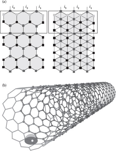
FIGURE 15.5 (a) 2D hexagonal and triangular arrays with three inputs. (A. Beg and V. Beiu, Ultra low power/energy SET-based Axon-inspired communication, 11th International Conference on Nanotechnology (IEEE Nano 2011), Portland, OR, pp. 1183–1186. © (2011) IEEE. With permission.); (b) 3D hexagonal communication array showing one voltage-gated ion channel (light dot) broadcasting (surrounding hemisphere) to the nearby voltage-gated ion channels. (V. Beiu et al., Minimizing communication power using near-neighbor axon-inspired lattices, Proc. IEEE-NANO, Portland, OR, 426–430. © (2011) IEEE. With permission.)
SETs are quantum-based devices relying on a Coulomb blockade [23]. Over the last 20 years, researchers have been looking into various logic gates built with SETs, while there has been very limited work on investigating the power and energy characteristics of such gates [45, 46, 47 and 48], and even less when going to the circuit and system levels [49]. Sulieman and Beiu [48] have successfully compared different SET-based full adders, including not only the delay and design complexity but also the sensitivity to variations using SIMON and MATLAB. SIMON is the most well-known simulator for SET devices and circuits [50]. It simulates co-tunneling using Monte Carlo and master equations, and has also been used for the simulations presented in this chapter.
The hexagonal and triangular arrays are presented in Figure 15.5a. Such arrays were also suggested in Refs. [14, 51], and preliminary results were reported in Refs. [15,16]. Based on the theorem presented in Section 15.3, the hexagonal array is expected to be more power- and energy-efficient than the triangular one. For the hexagonal array, the basic building block equivalent to the functioning of a voltage-gated ion channel is a two-input OR (OR-2) gate. Obviously, such an implementation will not emulate the self-timed shut-down mechanism of voltage-gated ion channels, and could end up wasting more energy as electrons are still going to be thrown away, while ions are recirculated. Similarly, for the triangular array, we will use a three-input OR gate (OR-3). We have designed and simulated both these gates using SIMON [50]. Both gates were built using an NOR gate followed by an INV, as can be seen in Figure 15.6. The OR-2 and OR-3 gates map directly onto the nodes (voltage-gated ion channels) of the arrays presented in Figure 15.5a.
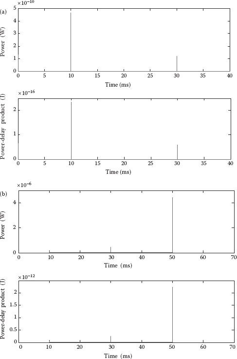
For mimicking an action potential propagating on an axon, we have decided to use pulses (spikes) that are 1 μs wide, spaced at 10 ms intervals. The sequence used for the input vectors for the OR-2 was as follows: 00 at 0 ms, 11 at 10 ms, 00 at 20 ms, 10 at 30 ms, and 00 at 40 ms. Similarly, the sequence for OR-3 was: 000 at 0 ms, 111 at 10 ms, 000 at 20 ms, 110 at 30 ms, 000 at 40 ms, 100 at 50 ms, and 000 at 60 ms.
FIGURE 15.6 SET-based OR gates (using SIMON): (a) OR-2 as a NOR-2 followed by an INV; (b) OR-3 as a NOR-3 followed by an INV. (A. Beg and V. Beiu, Ultra low power/energy SET-based Axon-inspired communication, 11th International Conference on Nanotechnology (IEEE Nano 2011), Portland, OR, USA, pp. 1183–1186. © (2011) IEEE. With permission.)
After performing the simulations, we have estimated the power and energy as
(15.22) |
where the supply voltage is VDD = 6.5 mV, i(t) is the instantaneous current (obtained from simulations), Pavg is the average power, and E is the energy. The total time for simulations was T = 40 ms for OR-2 and T = 60 ms for OR-3. The instantaneous P and E (as “power-delay-product”) for the OR-2 and the OR-3 gates are shown in Figure 15.7, while the numerical values for the different time intervals are presented in Tables 15.1 and 15.2.
An axon-inspired communication is an array-based communication link like those in Figure 15.5a, where all the nodes (voltage-gated ion channels) are transmitting the same data (i.e., either “0” or “1”). Interestingly, from Table 15.1, it can be immediately inferred that the transition from “00” to “11” exhibits lower power and energy consumption than the “00” to “10.” Similarly, for OR-3, we found the lowest P and E was for the “000” to “111” transition (see Table 15.2). We also found that the maximum values of P and PDP for the OR-3 gate are about 6 × higher than the ones for OR-2, while the minimum values of P and PDP for the OR-3 gate are about 5 × smaller than the ones for OR-2! This means that, if functioning perfectly (i.e., no errors), the OR-3 (to be used in a triangular array) would be more power and energy efficiency than a perfect OR-2 (to be used in a hexagonal array). This is counterintuitive as we were expecting that the hexagonal array which is using OR-2 gates would achieve lower power and energy than the triangular array using OR-3 gates, while our simulations show that it might be the other way around. Unfortunately, when errors occur, that is, transitions other than “000” to “111” to “000” appear, the OR-2 could become more efficient than OR-3. These results show that errors could be much dearer than one would expect, and suggest that a detailed combined power-reliability analysis is absolutely needed.
Finally, we are now in a position to make some rough estimates on the energy required for propagating data (communicating information) at a given distance. For CMOS, such information is taken from Ref. [52], from where it is known that transmitting a 64-bit word over 1 mm needs about 25 pJ. Therefore, sending one bit of information over a distance of 1 mm in current CMOS technology consumes 25 pJ/64-bit = 0.4 pJ/bit/mm (estimates of 4 nJ/cm have been reported for the brain [37]). To estimate the energy required by the two SET solutions (one based on a hexagonal array of OR-2 gates, and the other based on a triangular array of OR-3 gates), we consider the size of a SET transistor to be of about 1 nm (not only similar to the voltage-gated ion channels but also consistent with requirements for the room temperature operation [23]). An OR SET gate should occupy about 10 nm × 10 nm, while the distance between two SET gates is considered to be about 100 nm (from the known surface densities of various ion channels [19]). It follows that the number of SET gates covering a distance of 1 mm is 1 mm/100 nm = 10,000 SET gates. Structures like the arrays presented in Figure 15.5a would have 47,000 SET OR-2 gates (hexagonal array) and 70,000 SET OR-3 gates (triangular array). As reliability concerns might require more than three inputs in parallel, we estimate that about 100,000 SET gates per 1 mm are required for these axon-inspired transmission schemes. From Tables 15.1 and 15.2, the energy per SET gate if functioning correctly (without errors) is between 1.013E − 019 J (OR-3) and 4.77E − 019 J (OR-2) as the gates are going to transmit either all 0’s or all 1’s. It follows that a 1 mm SET-based communication would need 100,000 × 4.77E − 19 = 0.047 pJ/bit/mm (in fact, 47,000 × 4.77E − 19 = 0.022 pJ/bit/mm and 70,000 × 1.01E − 19 = 0.007 pJ/bit/mm, respectively). The main conclusion is that an axon-inspired communication like those presented in this chapter could be about 10 × (0.047 pJ/bit/mm vs 0.4 pJ/bit/mm) to 50 × (0.007 pJ/bit/mm vs 0.4 pJ/bit/mm) more energy-efficient than the current CMOS solutions, but depending strongly on reliability.
FIGURE 15.7 Power and energy (power-delay-product, or PDP) for the test sequence: (a) OR-2; (b) OR-3. (A. Beg and V. Beiu, Ultra low power/energy SET-based Axon-inspired communication, 11th International Conference on Nanotechnology (IEEE Nano 2011), Portland, OR, USA, pp. 1183–1186. © (2011) IEEE. With permission.)
This chapter aimed to identify the practical limits for ultra-low power/energy communications when using electronic principles. To this end, it has started by presenting a theoretical analysis supporting the fact that hexagonal arrays would be optimal to minimize communication power/energy consumption, because they are minimizing the number of nodes while maximizing the coverage area. Later, we have considered SET-based gates as the elementary building blocks for emulating axon-inspired locally connected arrays of voltage-gated ion channels. On the basis of simulations, we have found that axon-inspired SET-based solutions could offer energy savings in the range of 10 × to 50 × (over current CMOS solutions), while the particular logic gate used seems to play a significant role as the arrays themselves, with reliability being an open topic for further research. Finally, neither voltage-gated ion channels nor electronic nanodevices can be positioned very precisely; hence, they can never be located on the ideal positions suggested by the ideal arrays presented in this chapter. That is why the results reported here should be seen more like “a lower bound” on the power/energy required for nanoelectronic axon-inspired communications.
TABLE 15.1
OR-2 Average Power and Energy for Different Transitions
|
Input Vector |
|||
Time Interval (ms) |
From |
To |
Average Power (W) |
Energy (J) |
10–20 |
00 |
11 |
4.777E−017 |
4.777E−019 |
30–40 |
00 |
10 |
5.937E−016 |
5.937E−018 |
Source: A. Beg and V. Beiu, Ultra low power/energy SET-based Axon-inspired communication, 11th International Conference on Nanotechnology (IEEE Nano 2011), Portland, OR, USA, pp. 1183–1186. © (2011) IEEE. With permission.
TABLE 15.2
OR-3 Average Power and Energy for Different Transitions
|
Input Vector |
|||
Time Interval (ms) |
From |
To |
Average Power (W) |
Energy a (J) |
10–20 |
000 |
111 |
1.013E−017 |
1.013E−019 |
30–40 |
000 |
110 |
2.245E−015 |
2.245E−017 |
50–60 |
000 |
100 |
3.882E−015 |
3.882E−017 |
Source: A. Beg and V. Beiu, Ultra low power/energy SET-based Axon-inspired communication, 11th International Conference on Nanotechnology (IEEE Nano 2011), Portland, OR, USA, pp. 1183–1186. © (2011) IEEE. With permission.
This work was supported by two grants from UAEU (NRF RSA 1108-00329 and NRF RSA 1108-00451), by a British Council Prime Minister Initiative to Connect PMI2 grant (RC GS 271), by a grant from SRC (2011-RJ-2150G), and by a grant from Intel (2011-05-24G). This document is an output from the PMI2 Project funded by the UK Department for Innovations, Universities and Skills (DIUS) for the benefit of the United Arab Emirates Higher Education Sector and the UK Higher Education Sector. The views expressed are not necessarily those of the DIUS, or of the British Council.
1. International Technology Roadmap for Semiconductors (ITRS), SEMATECH, New York, NY, USA, 2011. Available at: http://public.itrs.net
2. J. D. Meindl, Q. Chen, and J. A. Davis, Limits on silicon nanoelectronics for Terascale integration, Science, 293, Sept. 14, 2001, 2044–2049.
3. V. Beiu, U. Rückert, S. Roy, and J. Nyathi, On nanoelectronic architectural challenges and solutions, Proc. IEEE-NANO, Munich, Germany, Aug. 2004, 628–631.
4. S. Rakheja and A. Naeemi, Interconnects for novel state variables, IEEE Trans. Electr. Dev., 57, Oct. 2010, 2711–2718.
5. R. W. Keyes, The wire-limited logic chip, IEEE J. Solid-State Circ., 17, 1982, 1232–1233.
6. R. W. Keyes, The power of connections, IEEE Circ. Dev. Mag., 7, 1991, 32–35.
7. J. A. Davis, R. Venkatesan, A. Kaloyeros, M. Beylansky, S. J. Souri, K. Banerjee, K. C. Saraswat, A. Rahman, R. Reif, and J. D. Meindl, Interconnect limits on Gigascale integration in the 21st century, Proc. IEEE, 89, 2001, 305–324.
8. V. Beiu, W. Ibrahim, and R. Z. Makki, On wires at low electron densities, Proc. IEEE-NANO, Genoa, Italy, Jul. 2009, pp. 703–706.
9. J. M. Rabaey, Beyond the horizon: The next 10× reduction in power—Challenges and solutions Proc. ISSCC’11, San Francisco, CA, USA, Feb. 2011. Plenary panel available at: http://isscc.org/doc/2011/ISSCC2011_PlenarySession4_slides.pdf and also http://isscc.org/videos/2011_plenary.html#session4
10. N. Magen, A. Kolodny, U. Weiser, and N. Shamir, Interconnect-power dissipation in a microprocessor, Proc. SLIP’04, Paris, France, Feb. 2004, pp. 7–13.
11. J. D. Meindl, Beyond Moore’s law: The interconnect era, Comp. Sci. Eng., 5, Jan. 2003, 20–24.
12. A. L. Hodgkin, and A. F. Huxley, A quantitative description of membrane current and its application to conduction and excitation in nerve, J. Physiol., 117, Aug. 1952, 500–544.
13. A. L. Hodgkin and R. D. Keynes, The potassium permeability of a giant nerve fibre, J. Physiol., 128, Apr. 1955, 61–88.
14. V. Beiu, Brain-inspired information processors, Intl. Forum on Minimum Energy Electr. Syst. (MEES2020), Abu Dhabi, UAE, May 2010. Available at http://grc.src.org/member/event/e003960/E003960_SessionV_Beiu.pdf
15. V. Beiu, L. Zhang, W. Ibrahim, and M. Tache, Minimizing communication power using near-neighbor axon-inspired lattices, Proc. IEEE-NANO, Portland, OR, USA, Aug. 2011, 426–430.
16. A. Beg and V. Beiu, Ultra low power/energy SET-based axon-inspired communication, Proc. IEEE-NANO, Portland, OR, USA, Aug. 2011, 1183–1186.
17. S. B. Laughlin and T. J. Sejnowski, Communication in neural networks, Science, 301, Sept. 2003, 1870–1874.
18. T. Albrecht, J. B. Edel, and M. Winterhalter, Special issue on new developments in nanopore research, J. Phys. Cond. Mat., 22, Nov. 17, 2010.
19. M. Hilt and W. Zimmermann, Hexagonal, square, and stripe patterns of the ion channel density in biomembranes, Phys. Rev. E, 75, 2007, art. 016202.
20. R. Phillips, T. Ursell, P. Wiggins, and P. Sens, Emerging roles for lipids in shaping membrane-protein function, Nature, 459, May 21, 2009, 379–385.
21. P. H. Nelson, A permeation theory for single-file ion channels: One- and two-step models, J. Chem. Phys., 134(16), Apr. 25, 2011, art. 165102.
22. M. Ø. Jensen, D. W. Borhani, K. Lindorff-Larsen, P. Maragakis, V. Jogini, M. P. Eastwood, R. O. Dror, and D. E. Shaw, Principles of conduction and hydrophobic gating in K+ channels, Proc. Natl. Acad. Sci., 107, Mar. 30, 2010, 5833–5838.
23. K. K. Likharev, Single-electron devices and their applications, Proc. IEEE, 87, Apr. 1999, 606–632.
24. W. A. Catterall, Ion channel voltage sensors: Structure, function, and pathophysiology, Neuron, 67, Sept. 2010, 915–928.
25. R. E. Dempski, K. Hartung, T. Friedrich, and E. Bamberg, Fluorometric measurements of intermolecular distances between the α- and β-subunits of the Na+/K+-ATPase, J. Biol. Chem., 281(47), Nov. 24, 2006, 36338–36346.
26. A. A. Faisal, and J. E. Niven, A simple method to simultaneously track the numbers of expressed channel proteins in a neuron, Proc. CompLife, Springer, LNBI 4216, 2006, pp. 257–267.
27. D. Attwell, and S. B. Laughlin, An energy budget for signaling in the grey matter of the brain, J. Cereb. Blood Flow Metab., 21, Oct. 2001, 1133–1145.
28. P. Lennie, The cost of cortical computation, Curr. Biol., 13, Mar. 18, 2003, 493–497.
29. K. Koch, J. McLean, R. Segev, M. A. Freed, M. J. Berry II, V. Balasubramanian, and P. Sterling, How much the eye tells the brain, Curr. Biol., 16(14), Jul. 25, 2006, 1428–1434.
30. H. Alle, A. Roth, and J. R. P. Geiger, Energy-efficient action potentials in hippocampal mossy fibers, Science, 325, Sept. 11, 2009, 1404–1408.
31. S. Bernèche, and B. Roux, Energetics of ion conduction through the K+ channel, Nature, 414, Nov. 1, 2001, 73–77.
32. E. Schneidman, I. Segev, and N. Tishby, Information capacity and robustness of stochastic neuron models, in S. A. Solla, T. K. Leen and K.-R. Müller (Eds.): Advances in Neural Information Processing Systems (NIPS’99), MIT Press, Cambridge, MA, 2000, pp. 178–184.
33. J. A. White, J. T. Rubinstein, and A. R. Kay, Channel noise in neurons, Trends Neurosci., 23(3), Mar. 2000, 131–137.
34. M. E. Raichle and D. A. Gusnard, Appraising the brain’s energy budget, Proc. Natl. Acad. Sci., 99(16), Aug. 6, 2002, 10237–10239.
35. S. Schreiber, C. K. Machens, A. V. M. Herz, and S. B. Laughlin, Energy-efficient coding with discrete stochastic events, Neural Comp., 14(6), Jun. 2002, 1323–1346.
36. N. Cohen, From ionics to energetics in the nervous system, Solid State Ionics, 176(19–22), Jun. 2005, 1661–1666.
37. P. Crotty, T. Sangrey, and W. B. Levy, Metabolic energy cost of action potential velocity, J. Neurophysiol., 96(3), Sept. 2006, 1237–1246.
38. B. C. Carter and B. P. Bean, Sodium entry during action potentials of mammalian neurons: Incomplete inactivation and reduced metabolic efficiency in fast-spiking neurons, Neuron, 64, Dec. 24, 2009, 898–909.
39. A. Hasenstaub, S. Otte, E. Callaway, and T. J. Sejnowski, Metabolic cost as a unifying principle governing neuronal biophysics, Proc. Natl. Acad. Sci., 107(27), Jul. 6, 2010, 12329–12334.
40. C. Howarth, C. M. Peppiatt-Wildman, and D. Attwell, The energy use associated with neural computation in the cerebellum, J. Cereb. Blood Flow Metab., 30(2), Feb. 2010, 403–414.
41. B. Sengupta, M. Stemmler, S. B. Laughlin, and J. E. Niven, Action potential energy efficiency varies among neuron types in vertebrates and invertebrates, PLoS Comput. Biol., 6(7), Jul. 2010, art. e1000840.
42. A. Singh, R. Jolivet, P. J. Magistretti, and B. Weber, Sodium entry efficiency during action potentials: A novel single-parameter family of Hodgkin–Huxley models, in J. Lafferty, C. K. I. Williams, J. Shawe-Taylor, R. S. Zemel, and A. Culotta (Eds.): Advances in Neural Information Processing Systems (Proc. NIPS’10), MIT Press, Cambridge, MA, 2011, pp. 2173–2180.
43. A. Moujahid, A. d’Anjou, F. J. Torrealdea, and F. Torrealdea, Energy and information in Hodgkin–Huxley neurons, Phys. Rev. E, 83, 2011, art. 031912.
44. B. N. Clark, C. J. Colbourn, and D. S. Johnson, Unit disk graphs, Discrete Math., 86, Dec. 1990, 165–177.
45. C. Choi, J. Lee, S. Park, I.-Y. Chung, C.-J. Kim, B.-G. Park, D. M. Kim, and D. H. Kim, Comparative study on the energy efficiency of logic gates based on single-electron transistor technology, Semicond. Sci. Technol., 24, May 2009, art. 065007.
46. V. Saripalli, V. Narayanan, and S. Datta, Analyzing energy-delay behavior in room temperature single electron transistors, Proc. VLSID, Bangalore, India, Jan. 2010, 399–404.
47. J. Lee, J. H. Lee, I. -Y. Chung, C. -J. Kim, B. -G. Park, D. M. Kim, and D. H. Kim, Comparative study on energy-efficiencies of single-electron transistor-based binary full adders including nonideal effects, IEEE Trans. Nanotech., 10, Sept. 2011, 1180–1190.
48. M. H. Sulieman, and V. Beiu, On single-electron technology full adders, IEEE Trans. Nanotech., 4, Nov. 2005, 669–681.
49. M. H. Sulieman, and V. Beiu, Characterization of a 16-bit threshold logic single electron technology adder, Proc. ISCAS, Vancouver, Canada, May 2004, pp. 681–684.
50. C. Wasshuber, H. Kosina, and S. Selberherr, SIMON—A simulator for single-electron tunnel devices and circuits, IEEE Trans. CAD IC Syst., 16, Sept. 1997, 937–942.
51. V. Beiu, The trustworthy wings of the mysterious butterfly, Intl. Nanotech. Conf. Comm. & Coop. INC6, Grenoble, France, May 2010 [Online]. Available at http://www.inc6.eu/presentations/We1-1_Beiu.pdf
52. W. J. Dally, The end of denial architecture and the rise of throughput computing (keynote), Proc. ASYNC, Chapel Hill, USA, May 2009 [Online]. Available: http://asyncsymposium.org/async2009/slides/dallyasync2009.pdf (also presented at HiPC’09 and DAC’09; see http://videos.dac.com/46th/wedkey/dally.html).