
An HDL Model of Magnetic Quantum-Dot Cellular Automata Devices and Circuits |
CONTENTS
17.1 Introduction
17.2 Review
17.3 HDL Framework
17.4 HDL Model of an MQCA Cell
17.4.1 I/O Interface
17.4.2 Magnetization
17.4.3 Propagation and Cell Placement
17.5 HDL Models of MQCA Building Blocks
17.5.1 MQCA Binary Wire
17.5.2 MQCA Majority Gate
17.5.3 MQCA-Specific Blocks
17.6 A Novel n-Input AND Gate in MQCA
17.7 Conclusion
Acknowledgment
References
Among the disparate emerging technologies that have been proposed to overcome the limitations of “end-of-the-roadmap” CMOS (complementary metal–oxide–semiconductor), quantum-dot cellular automata (QCA) shows promising features to achieve both high computational throughput and low-power dissipation. The QCA computational paradigm [1,2] introduces highly pipelined architectures with extremely high speed (of the order of THz), while radically departing from the switch-based operation of CMOS. QCA manufacturability has been demonstrated both for metal-dot QCA [3] and molecular scale allowing room temperature operation. Recently, magnetic QCA (MQCA) based on Co nanomagnets has been analyzed [4, 5, 6, 7 and 8]. The use of nanomagnets is very attractive because MQCA can operate at room temperature, and has been shown to be easier than the molecular implementation of an electrostatic QCA. Moreover, MQCA can also be integrated with other emerging technologies such as magnetic RAM for memory design. The clocking mechanism of MQCA is similar to electrostatic QCA; the use of abrupt switching in electrostatic QCA is unreliable [2] due to the possible generation of metastable states, so a quasi-adiabatic clocking scheme has been proposed to overcome the kink probability in QCA circuits [2]. For MQCA, a three-phase snake clock has also been proposed [9]. Finally, a technology-based solution has been proposed in Ref. [7] to stabilize the magnetization state of nanomagnets by adding biaxial anisotropy. This arrangement modifies the framework in which MQCA circuits can be designed, thus requiring further investigation into mechanisms (also at circuit level) to leverage the newly introduced functionalities.
In addition to the advances in cell manufacturing and fabrication, research at the higher circuit and system levels has been pursued for QCA. Various QCA architectural solutions have been proposed, such as memories [10,11] and microprocessors [12]. As for tools, QCADesigner [13] has been widely utilized by manually placing the electrostatic QCA cells on a two-dimensional layout and simulating their behavior. This is accomplished by solving the quantum equations describing the QCA circuit. However, owing to its low-level model, QCADesigner incurs high computational penalties and is not suitable to design or simulate logic circuits of even medium complexity; therefore, new environments suitable for CAD implementation must be devised for circuit-level QCA design. Hence, both a SPICE level model [14] and a simple VHDL level model [15] have been proposed for nanomagnet-based devices.
Ottavi et al. [16] have introduced an HDL-based design tool (HDLQ) that overcomes the limitations of simulators like QCADesigner with respect to a circuit-level evaluation for electrostatic QCA. In this chapter, an HDL framework (and associated tool) based on Ref. [7] is proposed as a viable support for the design of systems based on the MQCA nanodevices. The models of the proposed framework are compatible with the HDLQ framework and also provide a support to simulate the behavior of MQCA. The modeling proposed in this work is based on Ref. [7] and is valid until the underlying physical assumptions will be proven viable for the actual manufacturing of these devices. This framework utilizes different and novel models by which MQCA cells can be simulated and a circuit-level assessment can be pursued at reduced computational complexity compared with other (physically based) simulators, such as OOMMF. HDL models for a MQCA cell as well as building blocks are proposed to ensure magnetization, clocking, and signal propagation; functions and test benches are also presented for the proposed CAD tool (denoted by HDLM). Moreover, the lazy AND and the dictator gates are modeled to ensure correct MQCA operation. The effectiveness of the proposed tool is further evidenced by its application to the novel design presented in this chapter for an n-input AND gate.
This chapter is organized as follows: Section 17.2 provides an overview of MQCA; in Section 17.3, the basic principles of the proposed framework and tool (denoted as HDLM) are described. In Section 17.4, the HDL model of a MQCA cell is introduced in detail. Section 17.5 presents the functional model used in the HDL simulation for the MQCA building blocks. Some of these blocks (wire, majority voter) are similar to the electrostatic implementation, while others (the lazy AND and the dictator gate) are specific to an MQCA implementation. Section 17.6 introduces a novel n-input AND gate that exploits the characteristics and functionality of MQCA; this also shows the effectiveness of the proposed tool to investigate new gates while establishing at a functional level its operational features. The conclusion is provided in the last section.
QCA operates on a computational paradigm based on the interactions of a set of bistable cells. The two stable states of a cell lead to a straightforward correspondence with the logic (boolean) values of zero and one.
The initial proposal of electrical quantum-dot cellular automata (EQCA or just QCA) was based on the Coulombic interaction of arrays of cells or QCA cells. Each cell contains four quantum dots which trap two extra electrons. Coulombic interaction within the QCA cells is such that only two stable states are possible, that is, those in which the extra electrons occupy diagonally positioned quantum dots (Figure 17.1a). Through Coulombic interactions and an externally imposed clocking E-field, adjoining QCA cells are then able to transfer and process boolean operations or transfer information in Figure 17.1b in which the EQCA binary wire (i.e., the combination of cells that permits data transfer), inverter (i.e., the combination of cells that permits the inversion of the boolean value), and the majority voter (i.e., the combination of cells that permits one to perform the majority function F = AB + AC + BC) are depicted. EQCA cells, moreover, can be put in a metastable state through the E-field clock to process consecutive operations on the same cells; the possibility of having an inversion of the value stored on the cells (the so-called kink) is a function of the dimension of the clocking zones [17].
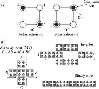
FIGURE 17.1 (a) Bistable feature of an EQCA cell (b) EQCA gates.
Recently, the QCA functional paradigm has raised attention when associated to magnetic devices in which the information is encoded in the magnetization state of the ferromagnetic devices. These devices (normally used for data storage) have shown to be particularly well suited also for logic functionality when included in architectures comparable to those used in QCA.
Cowburn and Welland [4] have realized MQCA operation by manufacturing chains of 110 nm diameter disk-shaped magnetic particles that manifest collective behavior. The magnetic anisotropy of the chains determines the preferred magnetization direction of disks and consequently the processing of binary information. Imre et al. [18] introduce a further shape-induced anisotropy with the creation of narrow nanomagnets on the scale of 10–100 nm. They can be assumed as single-domain magnets while still above the superparamagnetic limit. These elongated micromagnets are extremely stable given their shape-induced anisotropy. The magnetization points always to their long axis with two possible verses when no external magnetic field is induced. MQCA devices based on these magnets are expected to operate at room temperature and yield great promise for circuit design.
Similar to the EQCA functional paradigm, Figure 17.2a shows the two stable states of an MQCA cell (also referred to as a nanomagnet). An MQCA cell can also assume a metastable null state: while in the logic (zero and one) states, the magnetization is aligned to the vertical axis (which has a stable energy level), the magnetic field in the metastable state is aligned horizontally and does not interact with the neighboring cells (therefore, corresponding to a functionally null state).
Logic operation and signal propagation are performed in two steps in MQCA [7]. In the first step, all nanomagnets are aligned along their magnetically hard (lithographically short) axes by applying a global external magnetic field. In the second step, the external field is removed. If an input is imposed, then the dipole field alignment between the neighbors pushes them out of their metastable state and induces an antiparallel magnetization state. Therefore, the behavior of a horizontal line of MQCA cells can be viewed as a chain of inverters propagating the signal by successive operations (inversion) of the input value. Figure 17.2b shows the state of a chain of nanomagnets (binary wire) in its stable state.
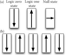
FIGURE 17.2 (a) Bistable feature of an MQCA cell (b) MQCA binary wire. (Copyright 2011 IEEE, with permission.)
Similar to the kink occurrence in electrostatic QCA, the cascade propagation in a horizontal wire may fail when the number of MQCA cells is increased [5]. To overcome this limitation, one of the most commonly used solutions requires the partition of an MQCA circuit into small zones driven by a suitable clock circuitry [8]. Carlton et al. [7] have proposed a solution to this problem; it introduces a hard axis stability by adding a biaxial anisotropy term to the net magnetization energy of each nanomagnet. Simulation performed using the OOMMF simulator [19] has shown that this technique allows a signal to correctly propagate up to 30 nanomagnets. When simulated, the input is transferred through 30 nanomagnets in 3 ns, corresponding to a propagation time through a single MQCA cell of approximately 100 ps. While a horizontal wire of nanomagnets tends to align in an antiparallel configuration, the vertical wire tends to align in parallel. Therefore, the horizontal wires invert the signal, while the vertical wires perform no inversion.
The basic logic gate for MQCA is still the majority voter and works in a similar fashion as for electrostatic QCA, that is, the output cell assumes the configuration of the majority of the inputs (Figure 17.3a). Together with the inversion provided by the antiparallel magnetization, this forms a functionally complete gate set.
Carlton et al. [7] have addressed the behavior of majority gates with legs of unequal length. The input that arrives earlier at the majority gate of Figure 17.3b imposes the magnetization on the center cell (crossing) of a majority gate. This may generate the wrong output and propagate an erroneous result also toward the other legs of the crossing. Figure 17.3b shows the propagation of information from the input nearest to the crossing toward the other inputs and to the output. A metastable (null) state is still present in those nanomagnets that have an equal distance from the inputs. To address the issues related to this race condition in the signals of the majority gate, Carlton et al. [7] have proposed two functional blocks:
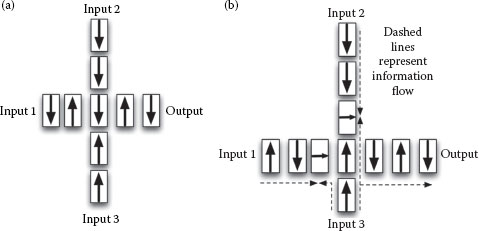
FIGURE 17.3 (a) MQCA majority gate (b) MQCA majority gate with uneven legs. (Copyright 2011 IEEE, with permission.)
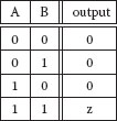
FIGURE 17.4 Truth table of lazy AND gate. (Copyright 2011 IEEE, with permission.)
1. Lazy AND: this gate acts as an AND gate when the output is supposed to be a logic zero. When the gate should output a logic 1, it generates no output, that is, the value of its output cell is in the metastable (null) state.
2. Dictator (majority) gate: this is a modified majority gate, in which the two vertical inputs (i.e., labeled 1 and 3) have a weaker coupling to the center nanomagnet (the nanomagnets are separated by a longer distance). It can only change the output provided all inputs agree; otherwise, the output toggles only once the value coming from the input labeled 2 reaches the center nanomagnet.
The lazy AND gate is physically realized by adding some extra nanomagnets (orthogonally placed with respect to the original direction) to block the magnetization corresponding to the logic one value. The truth table of the lazy AND is given in Figure 17.4. If one of the inputs is zero, then the output is zero; otherwise, the output remains in the metastable state (denoted as z, in analogy with the high impedance state of CMOS technology). By the truth table, the arrival order of the inputs is irrelevant. For example, assume that the A input signal arrives first: if A is zero, then the output is zero regardless of the value of B. However, if A is one, the gate will wait for the arrival of the input signal on B to decide whether the output must toggle to zero or remain in the metastable state.
For the dictator majority gate, the order in which the inputs arrive is important. Assume that the two vertical inputs and the single horizontal input are available; let the horizontal input be defined as dominant, that is, the distance of the horizontal nanomagnet from the center nanomagnet is smaller than the distance for the vertical nanomagnets. However, the magnetization of only one vertical input is not sufficient to toggle the majority gate. The vertical inputs can impose the value on the majority gate only if they arrive first and are identical. If only one vertical input reaches the center nanomagnet, or the vertical inputs are in disagreement (different values), then the gate remains in the z state. The horizontal input is capable of imposing the magnetization on the gate if the gate is still in the metastable state when the horizontal signal arrives. Using the lazy and the dictator gates, new and different logic gates can be designed; these gates are insensitive to the propagation delay of the signals. Figure 17.5 shows an AND gate that is insensitive to the order of arrival at its inputs.
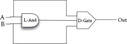
FIGURE 17.5 AND gate realized with dictator and lazy gates. (Copyright 2011 IEEE, with permission.)
The complexity of low-level physical simulations introduces more usable simulation models such as already proposed at SPICE-like level in Ref. [14] or at VHDL level in Ref. [15] in which a VHDL model for domain-wall-based devices has been proposed). This chapter proposes a novel HDL-based framework (with associated tool) by which MQCA can be assessed by simulation. The tool of the proposed HDL framework is referred to as HDLM due to its compatibility with a previous tool proposed by the same authors and applicable to electrostatic QCA design [16]. Modeling in HDLM relies on two components.
• A model for the MQCA cell as related to the unique features of this technology (such as magnetization) and its interaction with the immediate neighboring cells.
• The models for some basic building blocks for designing MQCA circuits. These building blocks include the majority voter as well as a few gates that are specifically used to alleviate some of the problems incurred in signal propagation by MQCA.
HDLM is compatible with HDLQ [16] because it uses similar principles and data structures; this permits primitives to be utilized as models for characterizing the cell and circuits, while changing the mode of operation from Coulombic interactions (for electrostatic QCA) to magnetization (for MQCA).
Similar to Ref. [16], the model is realized by using a Verilog HDL description of MQCA. The comparative advantages of such an approach are as follows:
1. OOMMF is not suitable to simulate circuits (even of modest size) due to the complexity of the equations involved in the MQCA cells.
2. The overall design process is highly simplified when an HDL description is used. Moreover, as HDL is widely used in the digital design community, many tools are available and compatible with this language and description.
Therefore, a Verilog description can be used to model the basic MQCA cell, and the structures described in the previous section, that is, the lazy AND and the dictator gates. HDL modeling allows the presence of an event-driven simulation to be leveraged, so, for example, the occurrence of transitions on a neighboring cell induces an event, and the evaluation of the next state in the cells. Consequently, by introducing a delay in updating the output of a cell, a cascade of switching events, as expected in a nanomagnet array, can be generated to model MQCA.
17.4 HDL MODEL OF AN MQCA CELL
This section describes the model for the behavior of an MQCA cell as introduced in the previous section. In HDLM, an MQCA cell requires a different characterization from the electrostatic cell of HDLQ. In particular, different functions must be utilized in the model to capture the magnetic properties of MQCA.
For an MQCA cell, we must define an I/O interface, that is, a model by which cell interactions occur among neighboring cells in the layout. In HDLM, this interface is characterized by the following features.
• Four inputs corresponding to the North, South, East, and West (N,S,E,W) directions.
• The input (called status) corresponding to the application of the external magnetic field that provides the metastable state.
• An output corresponding to the value assumed by the cell itself.
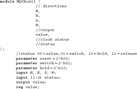
FIGURE 17.6 Interface of the Verilog code for an MQCA device.
While the N and S directions contribute to cell magnetization in a parallel manner, the E and W directions contribute in an antiparallel manner. Directional inputs and the output can assume three values, corresponding to the logic (zero and one) and to the metastable states (i.e., the z value).
Finally, the external magnetization field is considered to act as a clock signal and can assume the reset, switch, or hold values. If the clock signal is reset, the output of the cell is z, regardless of the value of the other inputs; otherwise, the Verilog model evaluates the magnetization of the cell by using a magnetization function based on the values seen at the directional inputs N, S, E, W.
The I/O interface of the Verilog module is presented in Figure 17.6. The module declares the above-mentioned inputs and outputs, and the parameters correspond to the possible states (reset, switch, hold) of the clock signal.
To evaluate the magnetization of the cell, a function converting the binary value to a magnetization value is used. The function bin2mag is given by
(17.1) |
The function bin2mag permits the magnetization of a cell to be evaluated by adding the magnetization values of the vertical inputs and subtracting the magnetization values of the horizontal inputs using
(17.2) |
The last step of this computation is the reverse conversion from the magnetization to the binary representation that follows from Equation 17.2. In Figure 17.7, the Verilog functions implementing the above two equations have been reported.
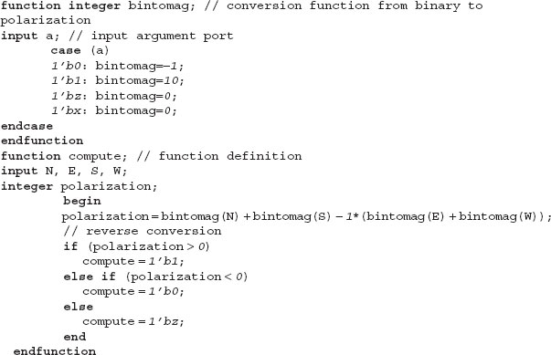
FIGURE 17.7 Verilog code for the magnetization functions.
17.4.3 PROPAGATION AND CELL PLACEMENT
To emulate the propagation delay through the nanomagnets, the output receives the computed value within a specified delay (set to a default value of 100 ps). The use of the magnetization function closely resembles the physics behavior. It has a high level of flexibility because it can be used to provide weights to the inputs (as discussed in a later section when the model of the dictator gate will be described). Figure 17.8 shows the Verilog code describing the propagation delay in the MQCA device.
Placement and connection between cells are performed as follows: the nanomagnets are placed on a grid layout, such that each magnet can have at most four neighbors, one for each direction. The directional inputs (N,S,E,W) are connected to the output of the corresponding neighbor, if present. If no cell is present in that direction, then the corresponding input is connected to a fixed z value. Finally, all cells are connected to a specific clock signal. The use of a clock signal is utilized to define the so-called clocking zones, similar to Ref. [9].
17.5 HDL MODELS OF MQCA BUILDING BLOCKS
HDL simulation models are presented in this section; MQCA building blocks, such as a wire, the majority gate, and the specific structures that have been proposed for MQCA (lazy AND and dominant majority gate), are assessed and evaluated.
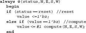
FIGURE 17.8 Verilog code for evaluation of the magnetization of an MQCA device.
The binary wire is a well-known block of the QCA functional paradigm. It is composed of a series of adjacent MQCA cells and allows the propagation of the information through the nanomagnets. Figure 17.9 shows the Verilog code of a horizontal MQCA wire. The MQCA cells making up the wire have been indexed with x and y coordinates in the two-dimensional grid layout. The signal connecting the output of a cell to the input of its neighbor is defined as a bidimensional wire. The output of the cell (with coordinates (x,y)) is connected to the signal v[x][y], while the west inputs are connected to v[x − 1][y] and the east input is connected to the v[x + 1][y] signal. The simulation starts by initially imposing an external magnetic field, corresponding to clock = “1,” thereby, forcing the z value to all cells. After the clock is lowered, the signal starts propagating in the west–east direction by the concatenation of events as triggered by the change in state of the neighboring cell located in the west (W) direction. Figure 17.10 shows its waveforms. Each output change occurs with the allowed switching time of a nanomagnet; currently, this is set to the default value of 100 ps delay, as reported in Ref. [7]. The wire behaves like the cascading effect of a domino chain; after all the cells are magnetized, the wire remains in a steady state until a new clock rising event erases the attained state.
A further building block that is modeled in HDLM is the majority gate. Figure 17.11 shows its MQCA layout; its inputs are positioned in the North, South, and West directions, while the output is in the East direction. The vertical inputs are noninverting, that is, only the horizontal input is inverting. In Figure 17.11, all inputs have the same length, and therefore they have the same delay. The waveform in Figure 17.11 shows the inputs, the values of the MQCA cells (for the input values to the majority gate), and the MQCA cells making up the wire that moves the computed value to the output. The signals arrive at the cell labeled Q22 at the same time, as expected for a correct functionality of the majority gate. Moreover, similar to the binary wire case, the waveforms show that for the majority voter also, a change in the inputs will not affect the computed value after the cells attain their final value.
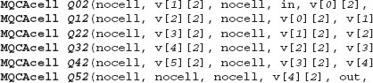
FIGURE 17.9 Verilog code of an MQCA wire. (Copyright 2011 IEEE, with permission.)
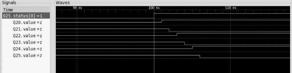
FIGURE 17.10 Waveform of an MQCA wire. (Copyright 2011 IEEE, with permission.)
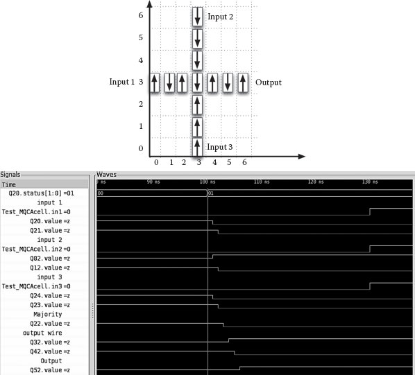
FIGURE 17.11 Layout and waveform of an MQCA majority gate. (Copyright 2011 IEEE, with permission.)
The functionality of the proposed simulation model in HDLM is extended to the MQCA-specific blocks (the lazy AND and the dictator gates).
1. Lazy AND gate: The lazy AND gate can be constructed from the majority gate by employing two modifications. The first modification consists of setting one of the inputs to the logic zero value to achieve an AND function with the remaining two inputs. The other modification is related to the computation of the so-called mag2bin function. As per the implementation of the lazy gate, the nanomagnet that computes the AND function can assume only a zero or z value, so the mag2bin function must be modified as per the following equation:
(17.3) |
The lazy AND gate can therefore be constructed as an MQCA cell with an input whose value is fixed at 0 and the mag2bin function is modified as in the above equation.
2. Dictator gate: The dictator gate can be considered as a modification of the majority gate. This gate is a majority gate that has vertical inputs at a distance further away than expected. Therefore, the interaction between the vertical inputs and the center of the majority gate is weaker. This behavior can be simulated by adding a weight in the magnetization function as given previously in Equation 17.2. As in accordance with Ref. [7], only when the vertical inputs have the same logic value, it is possible to impose a value at the output of the gate. When only one of the inputs is defined, or the two inputs have different values, then the output of the gate is in the z state. The modified magnetization function is given as follows:
(17.4) |
This function produces a value with magnitude greater than 0.5 when either the horizontal input is set, or the two vertical inputs have the same value. The corresponding mag2bin function can be expressed as follows:
(17.5) |
The above-described models have been implemented in Verilog and therefore can be used to simulate circuits as well as different gates as presented in the next section.
17.6 A NOVEL N-INPUT AND GATE IN MQCA
In this section, it is shown that the MQCA-specific building blocks introduced in the previous section together with HDLM can be used to design a novel MQCA gate, namely, an n-input AND gate. By leveraging the functional characteristics of MQCA with the lazy AND gate, a compact implementation of an n-input AND gate can be designed. This gate consists of two blocks.
• A block made of multiple lazy AND gates
• A block that resolves the output magnetization when all inputs are 1
The first block works similar to a wired AND gate, in which multiple lazy AND outputs are connected onto a single output wire (Figure 17.12 for n = 7). This makes the layout similar to a wired AND; when at least one input is 0, then the correspondent lazy AND output will dominate the magnetization on the output wire (because the other outputs will be in the so-called z state). When all inputs are equal to 1, the wired output remains in the z state; this condition is resolved by the second block referred to as the resolution block. The resolution block has the multiple lazy AND gate output and an additional input as inputs (denoted as “the longest input wire” in Figure 17.12). It generates a 1 as output if the additional input is 1 and the other input is z, 0 otherwise. This block is therefore made of the longest input wire and the output wire. According to the order of arrival of the inputs, the n-input lazy AND gate has no constraint (being composed of 2-input lazy AND gates), whereas the second block has to be designed such that the signal propagating on the longest input wire must always arrive after the result of the lazy AND wired function. This constraint can be accomplished by using a snake-shaped wire such as the one depicted in Figure 17.12. All inputs are placed in the W direction, while the output is in the E direction. The proposed AND gate has been described using the previously presented Verilog models and simulated to verify its correctness. The simulation results prove the functionalities of the proposed n-AND.
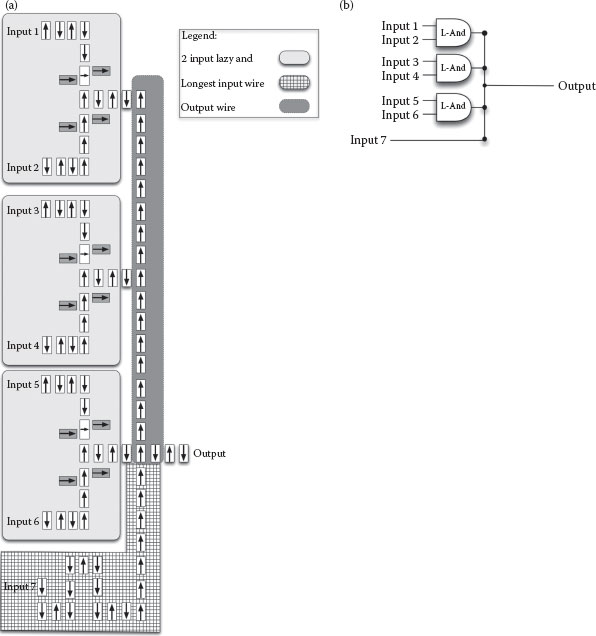
FIGURE 17.12 Layout and schematic of an n-input AND gate. (Copyright 2011 IEEE, with permission.)
This chapter has presented a new framework for analyzing MQCA devices and circuits; this framework has been implemented in HDL and a tool (HDLM) has been designed. In HDLM, the Verilog description has been implemented at the nanomagnet level to leverage the event-driven simulation engine ability of modeling a cascading propagation effect. Different weights are possible in HDLM to model the interaction between the neighboring magnets, thus allowing the operation of MQCA-specific functionalities (such as the lazy AND and the dictator gates) to be evaluated. With the proposed tool, it is possible to model and simulate not only the typical QCA paradigm building blocks but also the specific gates that have been introduced for MQCA. Finally, a novel MQCA gate (i.e., an n-input AND) has been introduced in this chapter; the operation of this gate has been simulated by utilizing HDLM. The proposed n-input AND gate exploits the novel characteristics of the MQCA functional paradigm and has been assessed using the proposed tool.
This research was partially funded by the Italian Ministry for University and Research; Program “Incentivazione alla mobilità di studiosi stranieri e italiani residenti all’estero,” D.M. n.96, 23.04.2001.
1. C.S. Lent, P.D. Tougaw, W. Porod, and G.H. Bernstein, Quantum cellular automata., Nanotechnology, 4(1), 49–57, 1993.
2. C.S. Lent and P.D. Tougaw, A device architecture for computing with quantum dots, in Proc. of the IEEE, 85, 541–557, 1997.
3. A.O. Orlov, I. Amlani, G.H. Bernstein, C.S. Lent, and G.L. Snider, Realization of a functional cell for quantum-dot cellular automata, Science, 277, 928–931, 1997.
4. R.P. Cowburn and M.E. Welland, Room temperature magnetic quantum cellular automata, Science, 287(5457), 1466–1468, 2000.
5. A. Imre, G. Csaba, G.H. Bernstein, W. Porod, and V. Metlushko, Investigation of shape-dependent switching of coupled nanomagnets, Superlattices and Microstructures, 34(3–6), 513–518, 2003, Proc. of the 6th Int. Conf. on New Phenomena in Mesoscopic Structures, Hawaii.
6. M.T. Alam, J. DeAngelis, M. Putney, X.S. Hu, W. Porod, M. Niemier, and G.H. Bernstein, Clocking scheme for nanomagnet QCA, in IEEE-NANO 2007, Hong Kong, Aug. 2007, pp. 403–408.
7. D. Carlton, N. Emley, E. Tuchfeld, and J. Bokor, Simulation studies of nanomagnet-based architecture, Nano Letters, 8(12), 4173–4178, 2008.
8. A. Kumari and S. Bhanja, Landauer clocking for magnetic cellular automata (mca) arrays, Very Large Scale Integration (VLSI) Systems, IEEE Transactions on, 99, 1–4, 2010.
9. M. Graziano, A. Chiolerio, and M. Zamboni, A technology aware magnetic QCA NCL-HDL architecture, in 9th IEEE Conference on Nanotechnology, 2009. IEEE-NANO 2009, Genoa, Italy, July 2009, pp. 763–766.
10. M. Ottavi, V. Vankamamidi, F. Lombardi, S. Pontarelli, and A. Salsano, Design of a QCA memory with parallel read/serial write, in VLSI, 2005. Proc. IEEE Comp. Soc. Annual Symp. on, May 2005, pp. 292–294.
11. M. Ottavi, V. Vankamamidi, F. Lombardi, and S. Pontarelli, Novel memory designs for QCA implementation, in 5th IEEE Conference on Nanotechnology, 2005, July 2005, pp. 545–548 vol. 2.
12. M.T. Niemier and P.M. Kogge, Logic in wire: Using quantum dots to implement a microprocessor, in The 6th IEEE International Conference on Electronics, Circuits and Systems, 1999. Proceedings of ICECS ‘99, Pafos, Cyprus, 1999, Vol. 3, pp. 1211–1215.
13. K. Walus, T.J. Dysart, G.A. Jullien, and R.A. Budiman, QCAdesigner: A rapid design and simulation tool for quantum-dot cellular automata, IEEE Trans. Nanotechnology, 3(1), 26–31, 2004.
14. G. Csaba, A. Imre, G.H. Bernstein, W. Porod, and V. Metlushko, Nanocomputing by field-coupled nanomagnets, Nanotechnology, IEEE Transactions on, 1(4), 209–213, 2002.
15. J.-O. Klein, E. Belhaire, C. Chappert, R.P. Cowburn, D. Petit, and D. Read, VHDL simulation of magnetic domain wall logic, Magnetics, IEEE Transactions on, 42(10), 2754–2756, 2006.
16. M. Ottavi, L. Schiano, F. Lombardi, and D. Tougaw, HDLQ: A HDL environment for QCA design, J. Emerg. Technol. Comput. Syst., 2(4), 243–261, 2006.
17. V. Vankamamidi, M. Ottavi, and F. Lombardi, Two-dimensional schemes for clocking/timing of QCA circuits, Computer-Aided Design of Integrated Circuits and Systems, IEEE Transactions on, 27(1), 34–44, 2008.
18. A. Imre, G. Csaba, L. Ji, A. Orlov, GH. Bernstein, and W. Porod, Majority logic gate for magnetic quantum-dot cellular automata, Science, 311(5758), 205–208, 2006.
19. M. J. Donahue and D. Porter, OOMMF User’s guide, Interagency Report NISTIR,, no. 6376, 1999, National Institute of Standards and Technology, Gaithersburg.