
CONTENTS
18.1 Introduction
18.2 Background
18.2.1 QCA Cell
18.2.2 Logic Gates in QCA
18.2.3 Clock Zones
18.2.4 Coplanar Wire Crossings
18.3 Restoring Binary Divider
18.3.1 Conventional Restoring Binary Divider Architecture
18.3.2 Restoring Array Divider for QCA
18.4 Implementation Details
18.4.1 Design Guidelines for Robust QCA Circuits
18.4.2 Implementation of the Restoring Divider
18.4.2.1 Basic Elements for Restoring Array Divider
18.4.2.2 Controlled Full Subtractor Cell
18.4.2.3 Comparison of Coplanar and Multilayer Wire Crossings
18.4.2.4 Timing Analysis
18.5 Simulation Results
18.5.1 Restoring Divider Results
18.5.2 Comparison Analysis of Dividers
18.6 Conclusion
Acknowledgment
References
Quantum-dot cellular automata (QCA) [1,2] is a promising emerging nanotechnology that may mitigate the problems that are anticipated for CMOS (complementary metal–oxide–semiconductor) due to the continued reduction of feature sizes. Since QCA operate according to different principles from CMOS technology, they require different design methods. Numerous nanoelectronic devices are being investigated and many experimental devices have been developed. DNA origami may serve as the interface between QCA circuits and CMOS systems on silicon substrates [3]. An architecture for data input into a molecular QCA circuit from an external CMOS circuit has been proposed [4]. The controlled formation and occupation of a new form of quantum-dot assemblies at room temperature have been demonstrated [5]. Furthermore, there is an attempt to integrate CMOS, single-electron transistors, and QCA [6].
High-level circuit design is needed to keep pace with the changing physical characteristics. Arithmetic units, especially adders, multipliers, and dividers, play an important role in the design of digital processors and application-specific systems.
Iterative computational circuit designs for QCA are difficult to build with conventional sequential circuit design methods that are based on state machines. State machines for QCA have problems due to long delays between the state machine and the units to be controlled. Even a simple 4-bit microprocessor that has been implemented with QCA [7] was made without using a state machine. Owing to the difficulty of designing sequential circuits, there has been little research into using QCA to realize iterative computational units, such as dividers. Most previous research has focused on simpler arithmetic unit designs, such as adders and multipliers.
This chapter presents a digit recurrent restoring binary divider. To use pipelining, an array structure is implemented in QCA. In Section 18.2, QCA cells and their operation as logic components are explained. In Section 18.3, the restoring binary divider design is presented. In Section 18.4, an implementation of the array restoring dividers using the proposed method is reviewed in detail. Finally, the simulation results and analysis of the designs and the summary are presented in Sections 18.5 and 18.6.
A semiconductor QCA cell has four quantum dots and two electrons that are trapped inside the cell. The electrons reside in the dots as shown in Figure 18.1. Binary information is encoded by the positions of the electrons, and a QCA cell allows two available polarizations, P = ±1. Since the quantum dots are coupled by tunnel barriers, the two electrons can change their positions freely by controlling the potential barriers using a clocking mechanism. The computation is performed by interactions based on Coulombic forces between neighboring QCA cells. Since the basic principle of operation is very different from CMOS, QCA “circuits” have many unique characteristics [8, 9 and 10].
The basic circuit elements in QCA are inverters and 3-input majority gates. All the other logic gates, such as AND gates and OR gates, can be realized using these basic elements. A conventional QCA inverter and its symbol are shown in Figure 18.2. Since the conventional inverter is large, several variations of the inverter have been developed as shown in Figure 18.3. The various inverters are used for the implementations in this chapter since their different relative positions of the input cells and the output cells are useful for circuit optimization.
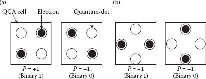
FIGURE 18.1 Basic QCA cells with two possible polarizations. (a) Regular cells, (b) 45° rotated cells. (S.-W. Kim and E. E. Swartzlander, Jr., Restoring divider design for quantum-dot cellular automata, IEEE 11th Conference on Nanotechnology (NANO-2011), Portland, OR, August 15–19, pp. 1295–1300. © (2011) IEEE. With permission.)
The 3-input majority gate in QCA is configured as shown in Figure 18.4. Its function is expressed using the following logic equation: M(A,B,C) = AB + BC + CA.
2-Input AND gates and OR gates are implemented by fixing one input of the majority gate as follows:
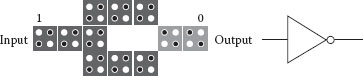
FIGURE 18.2 Layout and schematic symbol of a conventional inverter in QCA. (S.-W. Kim and E. E. Swartzlander, Jr., Restoring divider design for quantum-dot cellular automata, IEEE 11th Conference on Nanotechnology (NANO-2011), Portland, OR, August 15–19, pp. 1295–1300. © (2011) IEEE. With permission.)
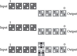
FIGURE 18.3 Layout of various inverters in QCA. (S.-W. Kim and E. E. Swartzlander, Jr., Restoring divider design for quantum-dot cellular automata, IEEE 11th Conference on Nanotechnology (NANO-2011), Portland, OR, August 15–19, pp. 1295–1300. © (2011) IEEE. With permission.)
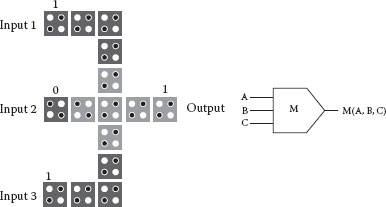
FIGURE 18.4 Layout and schematic symbol of a 3-input majority gate in QCA. (S.-W. Kim and E. E. Swartzlander, Jr., Restoring divider design for quantum-dot cellular automata, IEEE 11th Conference on Nanotechnology (NANO-2011), Portland, OR, August 15–19, pp. 1295–1300. © (2011) IEEE. With permission.)
While the logic optimization methods for CMOS can be used for QCA circuits, majority logic reduction methods specialized for QCA [11,12] are especially useful for circuits using XOR gates. For example, a full adder circuit can be implemented using only three majority gates and a few inverters.
All QCA cells are organized into clock zones. The designs in this chapter use four clock zones, and the computations are performed sequentially in the same order as that of clock zones. Each clock zone has a different clock signal as shown in Figure 18.5. When the clock signal is high, the potential barriers between the quantum dots are low and the polarization is 0. When the clock signal is low, the electrons in a QCA cell are localized and the polarization will be held as ±1. Using these 90° phase-shifted signals, each clock zone has one of four phase states among Switch, Hold, Release, and Relax. A QCA cells begins computing during the Switch state and holds the polarization during the Hold state. The QCA cell prepares for the next computing during the Release and Relax states. A QCA wire transfers information using clock zones as shown in Figure 18.6.
18.2.4 COPLANAR WIRE CROSSINGS
There are two kinds of wire crossings in QCA: coplanar wire “crossings” and multilayer crossovers. Coplanar wire crossings are implemented using only one QCA layer, which is an advantage. In contrast, multilayer crossovers require at least three layers for the wire crossovers and via interconnections. Since coplanar wire crossings currently seem more feasible for implementation, the dividers in this chapter are implemented using them. With multilayer crossovers, the full subtractor, multiplexer, and controlled full subtractor cells are slightly smaller than those designed with coplanar wire crossings. Coplanar wire crossings [13] are implemented using regular cells and 45° rotated cells as shown in Figure 18.7. Signals A and B can be transferred independently.
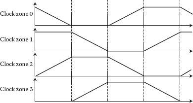
FIGURE 18.5 QCA clock signals for four clock zones. (S.-W. Kim and E. E. Swartzlander, Jr., Restoring divider design for quantum-dot cellular automata, IEEE 11th Conference on Nanotechnology (NANO-2011), Portland, OR, August 15–19, pp. 1295–1300. © (2011) IEEE. With permission.)
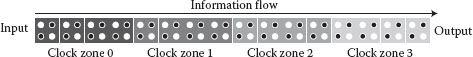
FIGURE 18.6 A QCA wire with clock zones. (S.-W. Kim and E. E. Swartzlander, Jr., Restoring divider design for quantum-dot cellular automata, IEEE 11th Conference on Nanotechnology (NANO-2011), Portland, OR, August 15–19, pp. 1295–1300. © (2011) IEEE. With permission.)
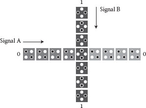
FIGURE 18.7 Example of a coplanar wire crossing. (S.-W. Kim and E. E. Swartzlander, Jr., Restoring divider design for quantum-dot cellular automata, IEEE 11th Conference on Nanotechnology (NANO-2011), Portland, OR, August 15–19, pp. 1295–1300. © (2011) IEEE. With permission.)
For signal B in Figure 18.7, the explanation is as follows. Empty dots (shown in white) have a charge of +½. Populated dots (in black) have a charge of +½ for the dot added to −1 for the electron, giving a total charge of −½. The input for the first cell in the path is 1. The lowermost quantum dot of the first QCA cell is empty, so it has a +½ charge; thus, an electron of the second QCA cell is attracted to the uppermost quantum dot of the second QCA cell. If the input is changed from 1 to 0, the lowermost quantum dot of the first QCA cell has −½ charge, so an electron at the uppermost quantum dot of the second QCA cell is repulsed. As a result, the state of the second QCA cell will be changed from 0 to 1, and so on.
Coplanar wire crossings are susceptible to sneak noise from neighbor cells and are very sensitive to geometric misalignment. To avoid such problems, careful implementation based on design guidelines for robust operation is required.
18.3.1 CONVENTIONAL RESTORING BINARY DIVIDER ARCHITECTURE
The division operations [14, 15 and 16] are performed in a bit sequential manner by the following formula:
where, i = 0, 1, 2, …, i − 1 is the recursion index, P(i) is the partial remainder in the ith iteration. D is the divisor, and r is the radix. In this chapter, r = 2. The initial partial remainder P(0) equals the dividend, and P(n) is the final remainder. Restoring division operates on fixed point fractional numbers and is based on the following assumptions:
0 ≤ P(i+1) < D, D < 1, the allowable quotient digits qi+1 are from the digit set {0,1}.
The quotient digit is selected by performing a sequence of subtractions and shifts. Each time, D is subtracted from the partial remainder r × P(i) until the difference becomes negative. Then, D is added back to the negative difference, which is called restoring. Since r = 2, the quotient digit is determined as follows:
The partial remainder is obtained by one left shift of P(i) and by one subtraction such that P(i+1) = 2P(i) − D. If it is positive, then qi+1 = 1, else qi+1 = 0 and one restoring addition is to be performed. The addition is needed to restore the correct partial remainder, P(i+1) = P(i+1) + D = 2P(i). Thus, performing binary restoring division requires at least one subtraction and may require one addition to determine each quotient bit. However, nonperforming restoring binary division needs only one subtraction per quotient bit because it uses a register to restore the partial remainder. Figure 18.8 shows a block diagram of a conventional restoring divider. This restoring divider starts with the dividend in the partial remainder register. If the correct quotient digit is a 0, the remainder is corrected by performing a compensating addition step. This scheme is not well suited to QCA implementation due to the delays of QCA wires.
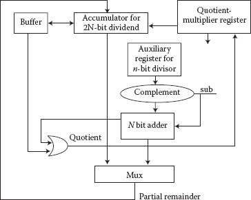
FIGURE 18.8 Restoring divider block diagram. (S.-W. Kim and E. E. Swartzlander, Jr., Restoring divider design for quantum-dot cellular automata, IEEE 11th Conference on Nanotechnology (NANO-2011), Portland, OR, August 15–19, pp. 1295–1300. © (2011) IEEE. With permission.)
18.3.2 RESTORING ARRAY DIVIDER FOR QCA
The design of high-speed iterative QCA arrays for parallel division uses a large amount of replicated units (for the comparison of the partial remainder and divisor) to reduce the number and size of QCA wires. The shift is realized by pipelined QCA wires. To improve the throughput of the array divider, pipelining can be used by inserting latches on the output of each row of cells. In general, a k × k restoring array divider receives a 2k-bit dividend and k-bit divisor, and produces a k-bit quotient and 2k-bit remainder including k leading 0s. Consider the division of a 2k × k restoring array divider with k = 3:
Figure 18.9 shows an example of a binary restoring divider. A block diagram of a 3 bit × 3 bit restoring array divider with controlled subtractor cells is shown in Figure 18.10. Each cell consists of a full subtractor and a two-input multiplexer that is the basic element, which is replicated n2 times to construct an n × n restoring array divider. When the control input P = 1, divider input d is subtracted from the partial remainder and the difference cellout is passed down to find the difference between the previous partial remainder and the divisor. Otherwise, when the control input P = 0, which triggers the multiplexer in a row cell, the partial remainder input bits are passed down unchanged.
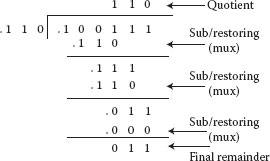
FIGURE 18.9 Example of a 3 bit × 3 bit binary restoring divider. (S.-W. Kim and E. E. Swartzlander, Jr., Restoring divider design for quantum-dot cellular automata, IEEE 11th Conference on Nanotechnology (NANO-2011), Portland, OR, August 15–19, pp. 1295–1300. © (2011) IEEE. With permission.)
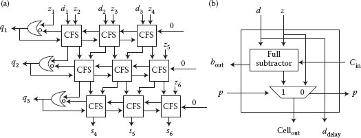
FIGURE 18.10 A 3 bit × 3 bit binary restoring divider. (a) Block diagram, (b) controlled full subtractor (CFS) cell. (Modified from S.-W. Kim and E. E. Swartzlander, Jr., Restoring divider design for quantum-dot cellular automata, IEEE 11th Conference on Nanotechnology (NANO-2011), Portland, OR, August 15–19, pp. 1295–1300 © (2011) IEEE.)
The difference , that is
Quotients qi are obtained from the left of each row. , where zi is the bit-shifted output in the (i − 1)th iteration. If zi = 1 or bout = 0, then the subtraction is performed.
18.4.1 DESIGN GUIDELINES FOR ROBUST QCA CIRCUITS
To design a robust circuit, the divider has been designed using coplanar wire crossings with the design guidelines suggested in refs. [17,18]. Coplanar wire crossings are used for this research since a physical implementation of multilayer crossovers has not been demonstrated yet. If multilayer crossovers are available for a design, the design can be implemented more efficiently. Robust operation of a majority of gates is attained by limiting the minimum and maximum number of cells that are driven by the output, which is verified using the coherence vector method. The maximum cell number for each circuit component in a clock zone is determined by simulations with sneak noise sources. For example, the maximum cell number for a simple wire is 14 and the minimum is 2.
18.4.2 IMPLEMENTATION OF THE RESTORING DIVIDER
18.4.2.1 Basic Elements for Restoring Array Divider
The restoring array divider is composed of controlled full subtractor cells that have one full subtractor and one two-input multiplexer. The full subtractor takes three inputs (Ai, Bi, and Ci) and produces two outputs (Di and Ci+1), where Di = Ai − Bi − Ci is the difference and Ci+1 is the borrow signal that carries from one cell to the next. A simplified majority expression for a subtractor design in QCA is
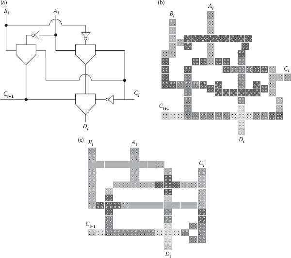
FIGURE 18.11 A full subtractor. (a) Schematic. (b) Coplanar crossing layout. ((a and b) Modified from S.-W. Kim and E. E. Swartzlander, Jr., Restoring divider design for quantum-dot cellular automata, IEEE 11th Conference on Nanotechnology (NANO-2011), Portland, OR, August 15–19, pp. 1295–1300 © (2011) IEEE.), (c) Multilayer crossover layout.
A full subtractor can be designed using only three majority gates and three inverters. Figure 18.11 shows the full subtractor schematic and layout. Both outputs of the full subtractor (i.e., the difference and borrow signals) have one clock latency with single and multilayer wire crossings. Simulation results are shown in Figure 18.12.
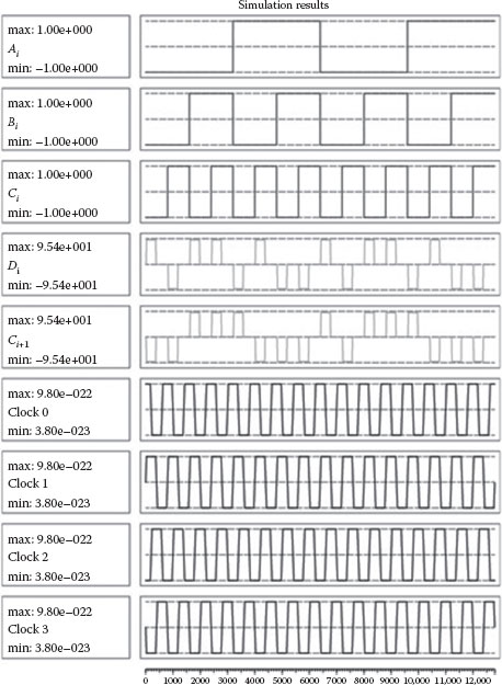
FIGURE 18.12 Simulation results of the full subtractor.
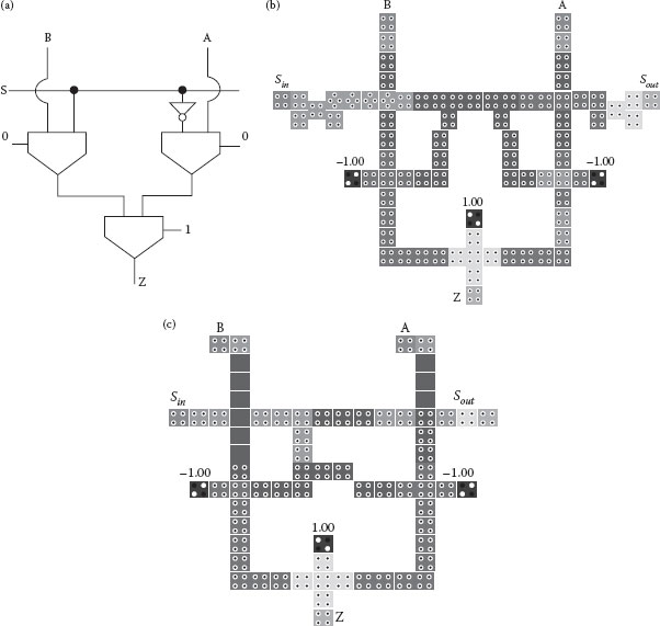
FIGURE 18.13 A 2:1 Multiplexer. (a) Schematic. (b) Coplanar crossing layout. ((a and b) S.-W. Kim and E. E. Swartzlander, Jr., Restoring divider design for quantum-dot cellular automata, IEEE 11th Conference on Nanotechnology (NANO-2011), Portland, OR, August 15–19, pp. 1295–1300. © (2011) IEEE. With permission.) (c) Multilayer crossover layout.
The two input multiplexer shown in Figure 18.13 is another cell element required for the controlled full subtractor cell. When the control signal S is 0, then input A comes out and when the control signal S is 1, then input B comes out with one clock latency.
18.4.2.2 Controlled Full Subtractor Cell
The CFS (controlled full subtractor) cell shown in Figure 18.14 basically conducts z − d if Pin = 1 to find the difference between the previous partial remainder and divisor. The borrow signal comes out after a two clock latency. Instead of shifting the partial remainder left to form 2P(i), the remainder is fixed and the divisor is shifted right along the divisor delay lines, and the quotient bits are obtained from the left of each row. This cell has the difference Di and borrow out Ci+1 with three clock latency and two clock latency, respectively. To make the array divider, this cell unit is modified for synchronization.
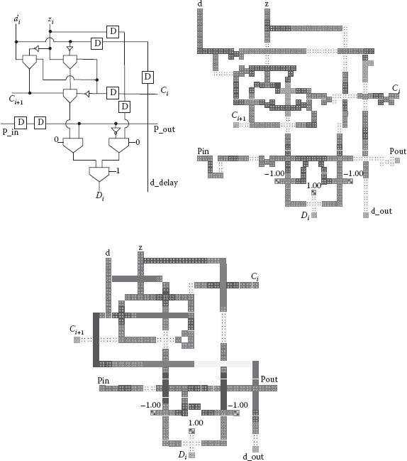
FIGURE 18.14 Controlled full subtractor cell. (a) Schematic. (b) Coplanar crossing layout. ((a and b) Modified from S.-W. Kim and E. E. Swartzlander, Jr., Restoring divider design for quantum-dot cellular automata, IEEE 11th Conference on Nanotechnology (NANO-2011), Portland, OR, August 15–19, pp. 1295–1300, © (2011) IEEE.) (c) Multilayer crossover layout.
18.4.2.3 Comparison of Coplanar and Multilayer Wire Crossings
Coplanar wire crossings are unique to QCA technology. With two cell types (regular and rotated), coplanar crossings can be realized. Many clock zones between the regular cells across the rotated cells are needed so the area will be large. Coplanar crossings are the current wiring method. Multilayer crossovers have some potential advantages such as latency and area minimization, but physical feasibility, assigning clock phases, and placement and routing are currently uncertain. Table 18.1 shows a comparison of the basic elements for a restoring divider with coplanar and multilayer wire crossings. With multilayer crossovers, each component has fewer cells and less area. Small elements such as the full subtractor and multiplexer have the same latency with both types of crossings, but the controlled full subtractor cell unit has slightly less latency when realized with multilayer wire crossings.
TABLE 18.1
Comparison of Basic Elements with Coplanar and Multilayer Wire Crossings
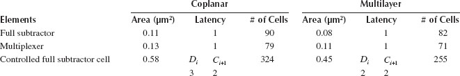
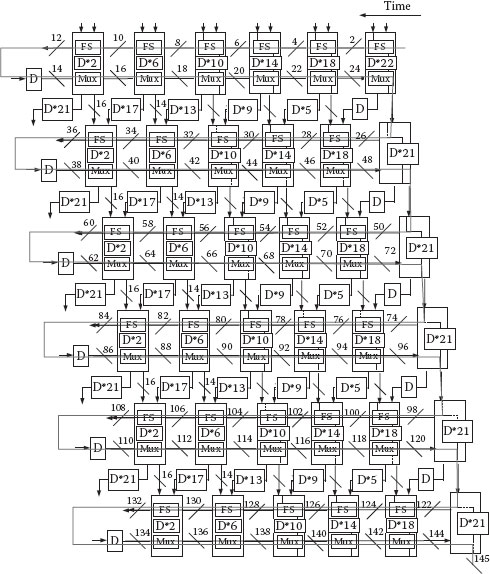
FIGURE 18.15 Timing block diagram for a 6 bit × 6 bit restoring array divider. (S.-W. Kim and E. E. Swartzlander, Jr., Restoring divider design for quantum-dot cellular automata, IEEE 11th Conference on Nanotechnology (NANO-2011), Portland, OR, August 15–19, pp. 1295–1300. © (2011) IEEE. With permission.)
The restoring array divider resembles an array multiplier, but it has different delay characteristics due to borrow signal propagation along the row and quotient signal feedback to each cell. From the rightmost column, CFS cells have 22, 18, 14, 10, 6, and 2 latches between the full subtractor and the multiplexer to implement the pipelining. Each cell has 21 delay latches for the divisor to pass down to the next row. A timing block diagram for a 6 bit × 6 bit restoring array divider is shown in Figure 18.15.
18.5.1 RESTORING DIVIDER RESULTS
Simulations were done with QCADesignerv2.0.3 [19] assuming coplanar wire crossings. The size of the basic quantum cell was set at 18 nm × 18 nm with 5 nm diameter quantum dots. The center-to-center distance is set at 20 nm for adjacent cells. The following parameters are used for a bistable approximation: 25,600 samples for the 3 bit × 3 bit restoring array divider, 156,000 samples for the 6 bit × 6 bit restoring array divider, 0.001 convergence tolerance, 65 nm radius effect, 12.9 relative permittivity, 9.8e–22 clock high, 3.8e–23 clock low, 1 clock amplitude factor, 11.5 layer separation, 100 maximum iterations per sample. The layout of the 3 bit × 3 bit restoring array divider is shown in Figure 18.16. Each cell with different delays is tested exhaustively, and the full integration is verified with input vectors: Dividend {39, 48, 42, 33, 36}, Divisor {6, 7, 6, 5, 5}. Correct output data come out from 37 clock latency as shown in Figure 18.17 such that Quotient {6, 6, 7, 6, 7} and Remainder {3, 6, 0, 3, 1}. The results are shown as integers to make it easier to understand even though they are fractions. The first consecutive division inputs are {100111, 110}, which are {39, 6} in decimal. .10011/.110 is expressed as the integer 0.609375/0.75. 0.609375 equals 0.75 times 0.75 (Quotient) plus 0.046875 (Remainder) and it is .110 and .000011 as the quotient and remainder fixed fractional numbers, respectively.
As the input word size increases, the number of RAS cells grows along the column lines in proportion.
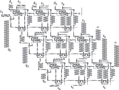
FIGURE 18.16 Layout of the 3 bit × 3 bit restoring array divider.
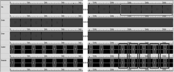
FIGURE 18.17 Simulation results of the 3 bit × 3 bit restoring array divider.
Figure 18.18 shows the layout of the 6 bit × 6 bit restoring array divider. The output waveform with 145 clock latency is shown in Figure 18.19. Six consecutive input vectors and outputs are:
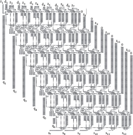
FIGURE 18.18 Layout of the 6 bit × 6 bit restoring array divider. (S.-W. Kim and E. E. Swartzlander, Jr., Restoring divider design for quantum-dot cellular automata, IEEE 11th Conference on Nanotechnology (NANO-2011), Portland, OR, August 15–19, pp. 1295–1300. © (2011) IEEE. With permission.)
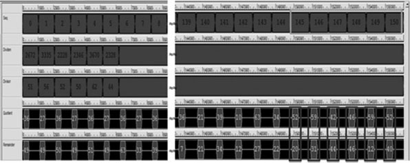
FIGURE 18.19 Simulation results of the 6 bit × 6 bit restoring array divider. (S.-W. Kim and E. E. Swartzlander, Jr., Restoring divider design for quantum-dot cellular automata, IEEE 11th Conference on Nanotechnology (NANO-2011), Portland, OR, August 15–19, pp. 1295–1300. © (2011) IEEE. With permission.)
TABLE 18.2
Comparison of QCA Dividers
Dividers |
Latency |
Area (μm2) |
# of Cells |
Throughput |
3 bit × 3 bit RAD |
37 |
15.05 |
6451 |
1 |
6 bit × 6 bit RAD |
145 |
86.22 |
42,236 |
1 |
12 bit × 12 bit RAD |
577 |
740.44 |
301,395 |
1 |
Source: S.-W. Kim and E. E. Swartzlander, Jr., Restoring divider design for quantum-dot cellular automata, IEEE 11th Conference on Nanotechnology (NANO-2011), Portland, OR, August 15–19, pp. 1295–1300. © (2011) IEEE. With permission.
18.5.2 COMPARISON ANALYSIS OF DIVIDERS
Table 18.2 shows a comparison of the 3 bit × 3 bit, 6 bit × 6 bit, and 12 bit × 12 bit QCA restoring array dividers. The dividers get much larger as the operand size increases. Also, the latency increases by almost a factor of 4 as the word size is doubled. Full simulation time took 42 h for the 12-bit restoring array divider. The restoring array divider has good throughput since an output is produced on every clock cycle after the 37th clock in the case of the 3 bit × 3 bit restoring array divider.
A digit recurrence restoring the binary divider design for QCA is presented in detail. It is a conventional design that uses controlled full subtractor cells to produce a relatively simple and efficient implementation. The design has been optimized for realization with QCA technology. The restoring array divider is implemented with CFS cell blocks. It can be easily enlarged by irregular block cells without long data connections, but it is large and has a long latency due to the restoring algorithm (recursive division). However, by using pipelining, it has a good throughput.
This chapter is an expanded version of Ref. [20]. Earl Swartzlander is supported in part by a grant from AMD, Inc.
1. C. S. Lent, P. D. Tougaw, W. Porod, and G. H. Bernstein, Quantum cellular automata, Nanotechnology, 4, 49–57, 1993.
2. C. S. Lent, P. D. Tougaw, and W. Porod, Quantum cellular automata: The physics of computing with arrays of quantum dot molecules, Proceedings of Workshop on Physics and Computation, Dallas, Texas, pp. 5–13, 1994.
3. M. Lieberman, DNA origami as circuitboards for QCA, 1st International Workshop on Quantum-Dot Cellular Automata (1WQCA), Vancouver, p. 8, Aug. 2009.
4. K. Walus, F. Karim, and A. Ivano, Architecture for an external input into a molecular QCA circuit, Journal of Computational Electronics, 8, 35–42, 2009.
5. M. B. Haider, J. L. Pitters, G. A. DiLabio, L. Livadaru, J. Y. Mutus, and R. A. Wolkow, Controlled coupling and occupation of silicon atomic quantum dots at room temperature, Physical Review Letters, 102, 046805, 2009.
6. A. A. Prager, A. O. Orlov, and G. L. Snider, Integration of CMOS, single electron transistors, and quantum-dot cellular automata, IEEE Nanotechnology Materials and Devices Conference, pp. 54–58, June 2009.
7. K. Walus, M. Mazur, G. Schulhof, and G. A. Jullien, Simple 4-bit processor based on quantum-dot cellular automata (QCA), 16th International Conference on Application-Specific Systems, Architecture and Processors, Samos, Greece, pp. 288–293, 2005.
8. C. S. Lent and P. D. Tougaw, A device architecture for computing with quantum dots, Proceedings of the IEEE, 85, 541–557, 1997.
9. M. T. Niemier and P. M. Kogge, Logic in wire: Using quantum dots to implement a microprocessor, The 6th IEEE International Conference on Electronics, Circuits and Systems, pp. 1211–1215, 1999.
10. M. T. Niemier and P. M. Kogge, Problems in designing with QCAs: Layout = timing, International Journal of Circuit Theory and Applications, 29, 49–62, 2001.
11. R. Zhang, K. Walus, W. Wang, and G. A. Jullien, A method of majority logic reduction for quantum cellular automata, IEEE Transactions on Nanotechnology, 3, 443–450, 2004.
12. W. Wang, K. Walus, and G. A. Jullien, Quantum-dot cellular automata adders, Third IEEE Conference on Nanotechnology, San Francisco, California, vol. 1, pp. 461–464, 2003.
13. D. Tougaw and C. S. Lent, Logical devices implemented using quantum cellular automata, Journal of Applied Physics, 75, 1818–1825, 1994.
14. A. B. Gardiner and J. Hont, Comparison of restoring and nonrestoring cellular-array dividers, Electronics Letters, 7, 172–173, 1971.
15. B. Parhami, Computer Arithmetic: Algorithms and Hardware Designs, 2nd Edition, New York, NY: Oxford University Press, Inc., 2010.
16. M. D. Ercegovac and T. Lang, Division and Square Root: Digit-Recurrence Algorithms and Implementations, Boston: Kluwer Academic Publishers, 1994.
17. K. Kim, K. Wu, and R. Karri, Towards designing robust QCA architectures in the presence of sneak noise paths, Proceedings of the Conference on Design, Automation and Test in Europe, Munich, Germany, pp. 1214–1219, 2005.
18. K. Kim, K. Wu, and R. Karri, The robust QCA adder designs using composable QCA building blocks, IEEE Transactions on Computer-aided Design of Integrated Circuits and Systems, 26, 176–183, 2007.
19. K. Walus, T. J. Dysart, G. A. Jullien, and R. A. Budiman, QCADesigner: A rapid design and simulation tool for quantum-dot cellular automata, IEEE Transactions on Nanotechnology, 3, 26–31, 2004.
20. S.-W. Kim and E. E. Swartzlander, Jr., Restoring divider design for quantum-dot cellular automata, IEEE 11th Conference on Nanotechnology (NANO-2011), Portland, OR, August 15–19, pp. 1295–1300, 2011.