
CONTENTS
19.1 Introduction
19.2 Theory and Advantages of LINA
19.3 LINA Logic Structures and Circuitry
19.3.1 LINA Logic Structures
19.3.2 Layout of LINA Blocks
19.4 LINA Design Space: Power, Speed, Reliability
19.5 Design Example: Design and Simulation of a Room Temperature, Reliability >0.99999 Full Adder
19.6 Conclusions
References
Researchers have been predicting limitations to the size scaling for CMOS (complementary metal–oxide–semiconductor)-integrated circuitry for many years. Often, these limits have been overcome and extended to smaller and smaller sizes [1]. However, as the CMOS minimum feature size has continued to shrink over the past decade, other concerns which are less fundamental and more practical have arisen. A particularly well-known example of this fact can be seen with limitations on the CPU clock speed due to power dissipation challenges. In response to this effect, CPU designers have resorted to techniques such as integrating multiple core CPUs in attempting to maintain the exponential computing performance growth which has driven the multibillion dollar industry for several decades. However, multi-core performance advantages also have limitations stemming from the ability to parallelize applications which will limit their effectiveness to increase practical performance [2]. In response to issues such as these, academia and industry have been researching alternative technologies to extend and replace CMOS designs in the coming years. However, these technologies have suffered from their own theoretical and practical challenges and thus a clear alternative for CMOS circuitry has not yet emerged.
One of the leading contenders to eventually replace CMOS is the quantum-dot cellular automata (QCA) nanoelectronics paradigm [3]. QCA have a relatively well-developed theoretical background in which THz switching of single nanometer molecular devices in a highly pipelined circuit architecture has been shown to be possible [4]. Additionally, alternate computing structures such as reversible logic [5] or systolic architectures [6,7] have been shown to be particularly well suited to be developed in the QCA framework. Advantages such as these provide the basis for continuing research into QCA as a potential replacement for CMOS designs; however, other pressing concerns must be addressed before large-scale integration and development can proceed.
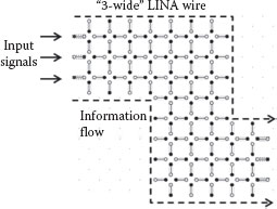
FIGURE 19.1 LINA wire (here shown with two 90° turns) with three “integrated signals.”
In particular, as with many other nanoelectronic proposals, reliability issues in the presence of room temperature thermal noise are a major concern due to the relatively small energies utilized to store and communicate data. Design alternatives which focus on increasing the reliability have tended to create additional problems for implementation. For instance, molecular QCA cells with sizes and cell spacing of ~1 nm have been proposed to raise state separation energies above the room temperature thermal noise and thus create reliable computing constructs [8]. However, at this ultra-small-size scale, practical difficulties arise, such as the layout of clocking wires necessary for the correct operation and functional pipelining of VLSI level QCA circuitry or power dissipation of circuitry with speeds, which create a reasonable alternative to current CMOS that will hamper near-term implementation prospects. Additionally, at this size, scale deposition and patterning of QCA logic structures will be very difficult and will require a significant advancement of current technologies before large-scale circuits could be generated [9]. Until issues such as these can be resolved, experimentation and demonstration of room temperature large-scale QCA circuitry may not be possible.
These issues have prompted research into other methods of increasing circuit reliabilities that are amenable to larger cells and structures required of currently available or near-term materials and circuit layout technologies. The lattice-based integrated-signal nanocellular automata (LINA)-type QCA [10] (shown in Figure 19.1), which offer potential solutions to many of these challenges are a result of this research. LINA is a lattice-based design that enables a mixture of self-assembly and patterning techniques to overcome deposition and/or positioning challenges and is flexible enough to incorporate error-prone fabrication and various clocking wire minimum pattern sizes. LINA designs were developed to enable utilization of self-assembled materials with relatively large inter-/intracellular spacings into reliable designs, thereby opening up a large area of currently implementable materials for circuit fabrication and room temperature operation. This chapter presents the theory and design of LINA circuitry along with simulation results to verify its design. Section 19.2 describes the underlying theory and advantages of LINA, Section 19.3 introduces logical structures and circuits, Section 19.4 presents design principles and simulation results, Section 19.5 offers a design example in which LINA is used, and the chapter concludes with Section 19.6.
19.2 THEORY AND ADVANTAGES OF LINA
One of the most pressing challenges facing the implementation of room temperature electric QCA in large reliable circuits is the precise deposition and patterning of single nanometer-sized molecules into structures which perform useful communication and logic. Single nanometer-sized molecules have been considered to be required to increase energy separation between ground and excited cell states above error-producing thermal noise. Proposals involving a mixture of self-assembly and patterning have offered hope to solve this challenge, but may have issues at the required size scales and integration levels [9]. In general, techniques to deposit and pattern molecules on the required size scale and with the precise placement of traditional QCA designs remain very difficult in the near term.
One reason for this difficulty lies in the traditional QCA cellular designs, and the resultant circuit layouts, which utilize some circuit design methods developed for other technologies. Lattice-based designs have recently been proposed [11], which attempt to solve the deposition issue by laying out cells based on common self-assembly formations, such as those shown in the nanoparticles of Ref. [12], thereby producing a method in which the relative cellular layout can be achieved. However, the ability to pattern large-scale complex circuit layouts on this small cellular size scale is not available for most large-scale lithography techniques. Additionally, the previous lattice-based designs do not account for common fabrication defects such as cell deletion, misalignment, or other fault mechanisms, commonly found with any self-assembly process. LINA attempts to advance the transition to lattice-based designs by incorporating additional “integrated signals” in communication and logic structures. This has the effect of increasing reliability by taking advantage of the inherent majority property of QCA to self-correct logical errors due to the previously mentioned error modes. The increased reliability also allows for larger cell sizes and cell spacings (possibly greater than 20 nm), which are able to be utilized for reliable room-temperature operation. This may allow for other larger nanoparticles, which can be more easily controlled, to be utilized in the role of a LINA QCA cell. Another added benefit of the LINA designs is the flexibility to adjust structure widths based on large-scale patterning technologies, thereby potentially allowing currently available patterning techniques to be used in LINA QCA circuits.
The integrated signals of the LINA designs carry common information much like the redundant designs would [13], but advance the concept by restoring and repairing signals continually and allowing for multiple paths for each individual signal. Additionally, owing to the unique geometries of these integrated signal designs, they do not require the condensation of multiple signals into a single wire or cell for input to logic. This is possible because LINA gates are able to accept each of the fully integrated-signal wires as separate inputs. This allows for robust communication and logic structures and removes weak points which are susceptible to logical faults.
The structure of the integrated signal wires can be seen in Figure 19.2, where three different possible wire widths are shown. The term “wire width” or “n-wide” is in reference to the number of integrated signals which are contained in the wire and not to its geometrical width. For example, the wire of Figure 19.2b has a width of 3 (making it a “3-wide” wire), even though the geometrical width is 7 times the lattice spacing. In general, LINA wires can be made into any odd integer number width providing design flexibility for increased reliability or to fit with clocking or patterning technologies.
One major difference between LINA and traditional QCA is that the information carried by LINA wires must be understood based not only on the cell state but also on the geometric position. Another added complexity arises from the fact that LINA utilizes two cellular orientations in the lattice arrangement. Therefore, in order to be able to quantify and study the operation of LINA wires and gates, a convention is developed based on the geometrical layout shown in Figure 19.3. In this convention, the binary state of the cell is determined by the position of the free electron (shown in the figure as the filled-in black dot location). When the electron is in a positive location, according to the axis parallel to the cell’s orientation, the cell is given a binary value of 1 and a polarization of +1. When the electron is in a negative direction, the cell is given a binary value of 0 and a polarization of −1.
The convention also dictates that the origin of the coordinate plane (0,0) is taken as the center cell of the input plane of a wire, regardless of the width of the wire. From there, the axes must be positioned along the directions of the two cellular orientations. This convention allows for the wire shown in the figure to be given the binary value of 1, due to the value of the cell at the coordinate origin. The scale of the axes is based on a common cellular lattice spacing (L), which directly corresponds to the eventual intercellular spacing, and along with the intracellular-dot spacing (D), provides the position of the cells’ component parts.
With this convention in hand, the expected binary value of the remaining cells of the wire can be obtained using Equation 19.1, where Vx,y is the binary value of the cell at position (x,y). For example, in Figure 19.3, the cell at position (0,0) has a binary value of 1 (V0,0 = 1). Therefore, using Equation 19.1, we can surmise the expected binary value of the cell at (2, −2) to be (V2,−2 = V0,0 = 1) because (−2 − 2)mod4 is equal to 0. Likewise, for the cell at (3,5), the expected binary value (V3,1 = not(V0,0) = 0) because (1 − 3)mod4 is equal to 2.
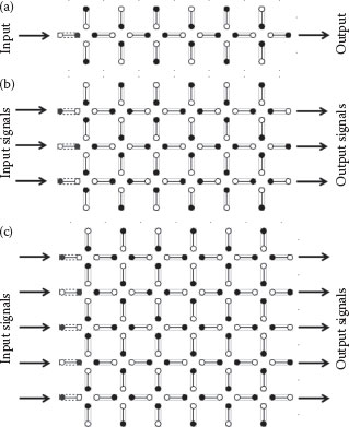
FIGURE 19.2 (a) 1-wide LINA wire, (b) 3-wide LINA wire, and (c) 5-wide LINA wire.
(19.1) |
In addition, the correct binary value of any true output plane of a LINA circuit will be the expected value of the center cell on the output plane. Furthermore, the total probability of correct logical output (PCLO) of this output can be obtained with knowledge of the individual PCLO of the cells on the output plane. The individual PCLOs are combined through the use of the probabilistic ensemble majority voting methods, such as shown the for a 3-wide wire in Equation 19.2 where “Pi” is the PCLO for Celli (here Cell1, Cell 2, and Cell3 are the output cells) and PTotal is the total output PCLO. For example, if the PCLOs of the three output signals in the wire in Figure 19.2b are 0.95, 0.97, and 0.95, then PTotal would be equal to 0.99465 according to
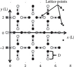
FIGURE 19.3 Geometrical layout convention used for LINA designs. The numbers of the scale are associated with integer multiples of the lattice spacing (L).
(19.2) |
Though there is an increase in the LINA design and/or layout complexity, as opposed to the traditional QCA, this is offset by the significant increase in reliabilities of LINA. An example of this reliability increase can be seen in Figure 19.4, which shows reliability numbers for two wires obtained by utilizing coherence vector simulation methods. As can be seen from the figure, a 300 nm wire created from cells with an inter-dot distance (D) equal to 10 nm and an intercellular lattice space (L) distance also equal to 10 nm was simulated. This wire shows a PCLO of 0.86 for the traditional QCA designs at a room temperature of 300 K. PCLO for the LINA designs are much improved at this temperature with the 1-wide LINA PCLO of 0.97, 3-wide PCLO of four 9’s (0.9999), and 5-wide PCLO of six 9’s.
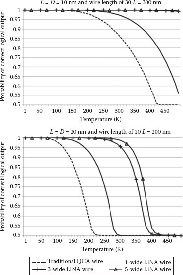
FIGURE 19.4 PCLO for traditional and LINA wires utilizing different cell sizes and spacings. (The simulations were performed with a relative permittivity of 1, a high clock level of 9.8e–20 J, and a low clock level of 3.8e–23 J.)
The predicted increase in room-temperature reliability is consistent for different L and D values (as well as for other simulation methods). PCLO for the room temperature operation of wires with L = D = 20 nm and overall length of 200 nm demonstrate this fact. Traditional QCA designs are nearly completely random (PCLO ~0.5) at this temperature. The 1-wide LINA PCLO is also nearly random here; however, the 3-wide LINA PCLO is 0.96 and the 5-wide PCLO is 0.98. The increase in reliability, especially for the larger spacings, allows for a greater number of potential implementation technologies compared to traditional QCA.
19.3 L INA LOGIC STRUCTURES AND CIRCUITRY
Traditional QCA logic design is centered on the three input majority voter gate, which is typically made up of a single QCA cell. This gate, along with the ability to invert a signal, gives the traditional QCA design logical completeness. The LINA designs are also based on the three input majority gate; however, the implementation of this logic gate requires a fully populated n × n area of the lattice map to perform computations (where the input and output wires are n-wide). The LINA majority gate performs the function in Equation 19.3 where the right input is being inverted in the majority gate of Figure 19.5. All LINA widths provide this same majority function as long as the center cell in the input wires is taken to be the logical value of the input.
(19.3) |
The same cellular structure is also used to provide a planer wire crossing for the LINA architecture. Also shown in Figure 19.5, the crossing structure requires a change in the clocking scheme for correct operation. This is accomplished with the application of an additional nontraditional clock signal to the cells in the crossing structure. The new clock only allows for signal pass-through and does not lend itself to a hold phase in which other cells are driven or a null phase in which other cells are unaffected. (The clock phases can be seen in the full adder design example of Section 19.5.) Additionally, for a correct functioning of the crossing, the two incoming wires must be 2 clock phases out of sync with each other. More information on this planer wire crossing can be found in Ref. [10].
Also required for logic completeness is an inverter structure—which in LINA can come in many forms. Owing to the inherent inverter chain nature of the LINA design, the simplest inverter can be achieved by carefully choosing the correct length of wire. However, this method of inverting a signal will be intolerant to even the slightest patterning errors and thus may not be the optimal choice for this function. Also, the method of controlling the length of the wire does not scale well to large circuitry where wires must meet at precise locations to perform logic with some of the inputs being inverted and some not. Instead, a dedicated LINA logic block to invert signals is preferred. The inverter block is created by removing a column in an otherwise normal LINA wire. An example of this technique can be seen in Figure 19.5.
Owing to the regular structure of the LINA lattice map and other clocking considerations, it is convenient (and in many ways necessary) to group LINA cells together when laying out circuitry. The majority gate and planer wire crossing of the previous section are examples of this grouping; however, wires should also be grouped in this way. This provides the advantage of allowing a simplified layout and design process as groups, or “blocks” of cells are used. Blocks are defined as squares of cells that have a length equal to the LINA design width. It should be pointed out that the width of the blocks and therefore the LINA design should be directly related to the layout technologies for the clocking structures as well as the cells themselves; therefore, intra-block cells should utilize the same clock phase. The first example of using blocks can be seen in Figure 19.5, and an example of using blocks to design a circuit will be seen in Section 19.5 in which a full adder design is produced.
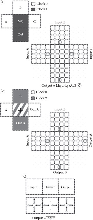
FIGURE 19.5 (a) 3-wide LINA majority gate and associated block diagram. (b) 3-Wide planer wire crossing and associated block diagram. (Clocking scheme for planer wire x-ing can be found in Ref. [10].) (c) 1-wide LINA inverter and associated block diagram. Note: Logical values of the input and outputs are taken at the cells circled.
19.4 LINA DESIGN SPACE: POWER, SPEED, RELIABILITY
It has already been shown how LINA designs can improve reliability by adding width to gates and wires. However, it is common to nanoelectronics proposals and QCA specifically that an increase in reliability is usually accompanied by an increase in power requirements. Certainly, adding additional cells to circuitry, in the form of LINA wires and gates, will create additional power which must be dissipated to the environment. However, LINA designs actually generate less heat for fixed desired reliabilities as opposed to reducing cell dimensions and spacing for the most relevant conditions. To prove this statement, formulas derived in Ref. [14] (and utilized in Ref. [15]) for power dissipation are utilized along with the LINA design tools. Concurrent evaluation of power, speed, and reliability is complicated by their interrelated nature and the fact that QCA cells both process and communicate information. This provides a rather difficult task in developing suitable metrics for quantifying the results of this evaluation.
Beginning by assuming a reasonable upper limit of power dissipation of 100 W/cm2, and that the average per cell power dissipation is evenly distributed throughout the cell, we are able to formulate a reasonable metric defined as the “effective QCA half-pitch.” This value is based on the distance between the basic QCA majority and fan-out gates (which utilize the same cellular structures and are elemental QCA logic components) as shown in Figure 19.7a. This quantity is not directly related to the CMOS half-pitch (which is based on the transistor as the elemental structure), but attempts to mimic the simplicity in understanding the CMOS metric coveys. The QCA effective pitch (Fp) is calculated in part by equating the power density of a single array block to our predefined limit of 100 W/cm2 as in
(19.4) |
with the length from the elemental logic device to the next along the side of a square being Fp (the “full” pitch), Nc being the number of QCA cells in the square of the full pitch, and Pc being the power per cell dissipated at a given clock frequency.
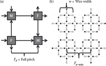
FIGURE 19.6 (a) Section of array of the majority (M) and fan-out (F) gates and associated pitch (Fp) to provide a metric for density, power, and speed considerations. (b) Example of the smallest 1-wide LINA array of elements. (IEEE-NANO) © (2011) IEEE. With permission.) (L. R. Hook IV and S. C. Lee. Lattice-based integrated-signal nanocellular automata (LINA) for the future of QCA-based nanoelectronics, 2011 IEEE Nanotechnol. Conf.
Lower limits to the pitch are calculated based on the smallest possible array block layout for any given cell spacing. Figure 19.6 shows an example of the smallest functional layout for a 1-wide LINA design. These two values give insight into the LINA design by revealing two areas of design space for a given cell and dot spacings and desired clock frequency in which the circuit density is either limited by power dissipation or by cell geometries. This space is shown in Figure 19.7b as the two segments of the line connecting the half-pitch values in all of the wire design lines.
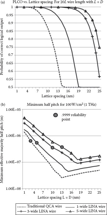
FIGURE 19.7 (a) PCLO for room temperature operation with increasing lattice spacing from 1 to 25 nm for traditional and 1,3,5-wide LINA wire designs. Wire length is 20L. (b) Minimum “effective majority” half-pitch for four traditional and LINA wire circuit design along with the 4 9’s reliability point at 1 THz. Note that the minimum half-pitch is seen with the 3-wide LINA design at this reliability. The simulations feeding these data were run with a relative permittivity of 1, a high clock level of 9.8e–20 J, and a low clock level of 3.8e–23 J.
TABLE 19.1
Minimum Half-Pitch and Wire Design for Various Clock Speeds and Reliabilities
Clock Speed |
Reliability >6 9’s |
Reliability >5 9’s |
Reliability >4 9’s |
1 THz |
590 nm |
517 nm |
360 nm |
L = 12 nm |
L = 13 nm |
L = 10 nm |
|
5-wide |
5-wide |
3-wide |
|
LINA |
LINA |
LINA |
|
500 GHz |
180 nm |
154 nm |
91 nm |
L = 10 nm |
L = 11 nm |
L = 13 nm |
|
5-wide |
5-wide |
5-wide |
|
LINA |
LINA |
LINA |
|
100 GHz |
15 nm |
12 nm |
9 nm |
L = 3 nm |
L = 4 nm |
L = 3 nm |
|
1-wide |
1-wide |
Traditional |
|
LINA |
LINA |
QCA |
Figure 19.7, as a whole, depicts data which are used in the process for determining the minimum half-pitch values based on reliability, power, speed, lattice spacing, and wire design. Figure 19.7a shows the reliabilities for various lattice spacings for four different wire designs (traditional, 1-wide LINA, 3-wide LINA, and 5-wide LINA) for a wire with length equal to 20 lattice spacings. This reliability is used to delineate various points along the half-pitch lines of Figure 19.7b to give minimum half-pitch for any desired reliability. Table 19.1 shows the calculated values for the half-pitch for various reliabilities based on this process. The table shows clear advantages for the LINA designs at high frequencies and with high reliability requirements. The data also show that the traditional QCA designs are advantageous in circuits where the desired frequency or reliabilities are low. (Further data reiterating these claims can be found in Ref. [10].)
It is interesting to see in Table 19.1 that the 1 nm cell spacing does not provide a minimum half-pitch for any of the entries. This is due in part to the number of cells and thus switching events that must be accounted for by using such relatively small cells and the large power per cell values which scale inversely with cell spacing due to higher kink energies. It is also interesting to note that simulations involving QCA designs do not yield a particular small circuit area if 1 THz switching with high reliabilities is desired; instead, a trade-off between circuit area, clock frequency, and reliability will have to be made. These types of trades are common for IC designers even today, and as technologies improve, these trades are sure to grow more favorable.
19.5 DESIGN EXAMPLE: DESIGN AND SIMULATION OF A ROOM TEMPERATURE, RELIABILITY >0.99999 FULL ADDER
As an example of LINA designs and how the results found in the previous sections may be used, consider the design of a full adder with greater than 5 9’s reliability at 100 GHz clock speed. Table 19.1 shows that for this speed and reliability, 1-wide LINA provides the greatest space/power efficiency using a 4 nm spaced LINA circuit. Many circuits will be restricted by the material implementation and thus will not be able to precisely choose lattice spacing. Additionally, owing to the low reliabilities for the smaller width designs with spacings larger than a few nanometers, such as traditional QCA or 1-wide LINA, larger width designs may be necessary. However, for this example, the ability to precisely define spacings will be assumed to demonstrate the use of Table 19.1.
The full adder design chosen is based on the simplified full adder sum and carry outputs from Ref. [16]. The logical schematic of the full adder design which was chosen can be seen in Figure 19.8a. Figure 19.8b shows the LINA blocks design which can be used to implement the full adder with any width of the LINA circuit as has been discussed. The blocks are labeled with either the input (A, B, or C) or the block function (M for majority, X for crossing, or I for inversion). Additionally, the circuit uses a simple design rule which dictates a single block spacing between adjacent wires, although it may need to be changed based on the specifics of the implementation technologies. Figure 19.8c shows the 1-wide 4 nm LINA layout for the circuitry corresponding to the blocks design. The sum and carry-out outputs are taken from the bottom of the circuit and are valid for one complete clock cycle after the corresponding inputs are latched in, as can be seen by the simulation results of Figure 19.8d. Another important feature of this particular full adder design is the use of five LINA coplanar wire crossing blocks and both LINA wire crossing clock patterns. As can be seen in the diagrams, the coplanar crossings are able to pass signals which are half a clock out of phase with each other (clocks 0 and 2 or clocks 1 and 3). The clock signals which allow this are shown along with the traces for all of the other clock signals in Figure 19.8e. Overall, the proposed full adder circuit takes up an area equal to 16 × 14 blocks. The actual area per block is dependent on the lattice spacing used as well as the width of the LINA wire. Overall, the 4 nm 1-wide full adder uses 91 blocks and 553 LINA cells and encompasses an area of 256 nm × 192 nm = 49152 nm2 and one full clock cycle for complete operation.
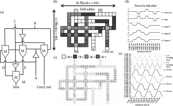
FIGURE 19.8 (a) Logical schematic of the full adder cell with majority logic reduction. (b) LINA blocks the layout of a full adder. (c) 1-wide LINA layout of a full adder circuit. (d) Traces for the inputs and outputs of a full adder circuit. (e) Clock traces used for the full adder.
As has been briefly mentioned, the blocks design for this full adder can be implemented with any width of LINA wire. To accomplish this, each block must encompass a completely populated n × n square area of the LINA lattice map with the length of the block equal to the width of the LINA wire. Therefore, LINA designs are able to be directly scalable as implementation technologies improve.
If the QCA paradigm is to compete as a suitable replacement for CMOS-integrated circuitry in the coming years, implementation strategies for large-scale room-temperature operation must be developed. Traditional QCA designs make this difficult due to size restrictions for highly reliable components and both cellular and circuit layout geometries. Lattice-based integrated-signal nanocellular automata (LINA)-type QCA offer an alternate design strategy which is more amenable to currently available or near-term nanoparticle implementation technologies by adhering to lattice maps (which fit more directly with self-assembled materials) and allowing for flexible wire widths to adjust to the resolution of large-scale patterning technologies. LINA have also been shown to increase the reliability in the presence of thermal excitations and assembly or patterning errors, thereby increasing the potential for room-temperature operation and near term fabrication of cellular automata-based computing systems. With these facts in mind, this chapter has begun to build a foundation upon which LINA logical devices can be designed. This has been accomplished by developing a logically complete set of primitives, including a LINA majority gate, inverter, and a planer wire crossing structure. LINA designs have also been evaluated in terms of the power/speed/reliability/area trades and shown to be advantageous compared to traditional QCA designs in this respect. As an example of the LINA design process, a LINA full adder was designed, laid out, and simulated with good results. Taken together, this chapter provides an important foundation to the logical design of LINA devices, thus adding depth to a strategy that offers hope for large-scale room temperature implementation and continued viability of the QCA paradigm to supplement and/or replace CMOS in the near future.
1. International Technology Roadmap for Semiconductors (ITRS) 2010 Update, http://www.itrs.net/Links/2010ITRS/Home2010.htm, 2010.
2. H. Sutter, The free lunch is over: A fundamental turn toward concurrency in software, Dr. Dobb’s Journal, 30(3), 202–210, 2005.
3. P. D. Tougaw and C. S. Lent, Logical devices implemented using quantum cellular automata, J. Appl. Phys., 75, 1818–1825, 1994.
4. J. Timler and C. S. Lent, Power gain and dissipation in quantum-dot cellular automata, J. Appl. Phys., 91(2), 823–831, 2002.
5. H. Thapliyal and N. Ranganathan, Reversible logic-based concurrently testable latches for molecular QCA, IEEE Trans. Nanotechnol., 962–969, 2010.
6. A. Fijany, B. Toomarian, and M. Spotnitz, Novel highly parallel and systolic architectures using quantum dot-based hardware, Parallel Comput., 484–492, 1999.
7. L. Lu, W. Liu, M. O’Neill, and E. E. Swartzlander Jr., QCA systolic matrix multiplier, 2010 IEEE Annual Symposium on VLSI, Belfast, UK, pp.149–154, 2010.
8. Y. Wang and M. Lieberman, Thermodynamic behavior of molecular-scale quantum-dot cellular automata (QCA) wires and logic devices, IEEE Trans. Nanotechnol., 3, 368–376, 2004.
9. W. Hu, K. Sarveswaran, M. Lieberman, and G. H. Bernstein, High-resolution electron beam lithography and DNA nano-patterning for molecular QCA, IEEE Trans. Nanotechnol., 4, 312–316, 2005.
10. L. R. Hook IV and S. C. Lee, Lattice-based integrated-signal nanocellular automata (LINA) for the future of QCA-based nanoelectronics, 2011 IEEE Nanotechnol. Conf. (IEEE-NANO), 2011.
11. L. R. Hook IV and S. C. Lee, Design and simulation of 2-D 2-dot quantum-dot cellular automata logic, IEEE Trans. Nanotechnol., 10, 996–1003, 2011.
12. E. V. Shevchenko, D. V. Talapin, N. A. Kotov, S. O’Brien, and C. B. Murray, Structural diversity in binary nanoparticle superlattices, Nature, 439, 55–59, 2006.
13. T. Dysart and P. Kogge, Reliability impact of N-modular redundancy in QCA, IEEE Trans. Nanotechnol., 10, 1015–1022, 2011.
14. J. Timler and C. S. Lent, Power gain and dissipation in quantum-dot cellular automata, J. Appl. Phys., 91(2), 823–831, 2002.
15. S. Srivastava, S. Sarkar, and S. Bhanja, Estimation of upper bound of power dissipation in QCA circuits, IEEE Trans. Nanotechnol., 8, 116–127, 2009.
16. R. Zhang, K. Walus, W. Wang, and G. A. Jullien, A method of majority logic reduction for quantum cellular automata, IEEE Trans. Nanotechnol., 3, 443–450, 2004.