
Sensing and Writing Operations of Nano-Crossbar Memory Arrays |
CONTENTS
22.1 Introduction
22.2 Reading Operation of Crossbar Arrays
22.2.1 Voltage Configurations for Reading Operation
22.2.2 Sensing Margin
22.2.3 Disturbance and Power Efficiency
22.3 A Crossbar Array Solution Based on Matrix Algebra
22.4 Effect of Nonlinear Memory Characteristics
22.5 Writing Operation of Crossbar Arrays
22.6 Discussions and Summary
References
Many nanoarchitectures are based on the crossbar arrays where active devices are built at the junctions between access lines laid out in orthogonal arrangement [1]. NanoFabrics [2], nanoscale programmable logic array (NanoPLA) [3], and nanoscale application-specific integrated circuit (NASIC) [4] are some examples of the two-dimensional (2D) crossbar-based nanoarchitectures. Crossbar arrays can also be built on top of CMOS (complementary metal–oxide–semiconductor) to implement three-dimensional (3D) architectures such as CMOS/nanowire/molecular (CMOL) [5] or field-programmable nanowire interconnect (FPNI) [6]. These hybrid nanoarchitectures can utilize both the computation power of CMOS and the high-density data storage and signal-routing capabilities of crossbar arrays. Crossbar array architectures attract great attention in the development of molecular electronics [7, 8, 9 and 10]. Some molecule-based devices have different resistance states and can be electrically switching between them. The resistive network of these devices can be built as crossbar arrays to implement logic and memory functions. The simple structure of crossbar arrays may enable the bottom-up self-assembly process to achieve low fabrication cost [11].
With the CMOS-based flash memories quickly approaching the scaling limit, several novel memory concepts have emerged as potential candidates for the next-generation nonvolatile memories [12]. Most of these emerging memories are simple two-terminal devices, which are also compatible with crossbar array architectures. By building memory devices at the crossing points of horizontal and vertical access lines, a footprint as small as 4F2 (F: feature size of a technology node) can be achieved. In recent years, there has been a strong demand for high-density and low-cost solid-state memories driven by data-intensive consumer applications. Crossbar memory arrays and their 3D stacks have been considered as promising solutions in this direction. An eight-layer one-time-programmable memory was demonstrated using the crossbar arrays of antifuse/diode memory devices [13]. More recently, multilayer-programmable memory was also demonstrated on oxidebased nonlinear resistive switching memories [14]. Phase-change memory has also been integrated in crossbar arrays with two-terminal select devices [15, 16 and 17].
A well-known challenge with crossbar arrays is the large amount of parasitic leakage paths (i.e., sneak paths). When accessing a selected device in the array, the sneak paths formed by unselected devices degrade the sensing margin and the effective voltage/current delivered to the selected device. At the same time, the unselected devices are also exposed to the operation voltages which may cause an unexpected disturbance. Select devices with rectifying behaviors can help to reduce parasitic leakage and disturbance. However, two-terminal select devices (e.g., diodes) compatible with both crossbar architectures and the switching requirements are still under research. Low processing temperature is also required on these devices for 3D memory architectures, which constrains the available select device options. Passive crossbar arrays without select devices provide a baseline for analysis and benchmark [18, 19 and 20]. Therefore, this chapter discusses the reading and writing accessibility of passive crossbar arrays, using both an analytical approach and a statistical simulation method, to discuss the effects of key device and array parameters on crossbar array operations.
The reading operation of a crossbar array needs to maximize the sensing margin defined as the output signal difference between different states of a selected device. The writing operation requires a sufficiently high voltage and current to be delivered to a selected device. At the same time, both operations need to minimize the disturbance on unselected devices, as well as to maximize the speed and power efficiency. The accessibility of a crossbar array is determined by the feasibility and efficiency of the reading and writing operations.
This chapter is organized into the following sections. Section 22.2 provides a detailed analysis on the reading operation of crossbar arrays based on circuit simplification and analytical solutions. It will show that the voltage configurations and sensing method determine the accessibility of crossbar arrays. Section 22.3 introduces a matrix-based solution applicable to general resistance distributions in crossbar arrays. Statistical analysis can be developed based on the large number of random resistance patterns. Section 22.4 discusses the feasibility of improving the accessibility of crossbar arrays using nonlinear memory device characteristics. The writing operation of crossbar arrays will be analyzed in Section 22.5. The last Section 22.6 will summarize this chapter.
22.2 READING OPERATION OF CROSSBAR ARRAYS
Many emerging memory devices exhibit resistive switching characteristics, that is, their resistance can be electrically switched between a high-resistance state (HRS, or off-state) and a low-resistance state (LRS, or on-state). The switching from HRS to LRS is usually called the “set” and that from LRS to HRS the “reset.” Logic information is encoded in these different resistance states (e.g., HRS for logic “0” and LRS for logic “1”). The analysis in this chapter starts with simple linear devices with constant HRS and LRS resistances, that is, Roff and Ron, respectively. The on/off ratio (Roff/Ron) is an important parameter for an array sensing margin. It will be shown later that when appropriate nonlinearity exists in the current–voltage (I–V) characteristics in HRS and LRS, the sensing margin may be improved.
Figure 22.1 illustrates a crossbar array with m wordlines (WLs) and n bitlines (BLs). For simplicity, the WL and BL resistance is ignored in this analysis. Take the Cu interconnect as an example. It is estimated that for the feature size down to 22 nm, the line resistance between neighboring devices is ~0.2 Ω [21]. For memory devices with LRS resistance above 20 kΩ and WL/BL lines with less than 1000 devices, the total line resistance is below 1% of memory device resistance and may be ignored in the first-order analysis. However, for memory devices with lower operating resistance, interconnect lines with higher resistivity, and larger arrays, line resistance may not be negligible in accurate analysis. Quantitative solutions including line resistance are more complex.
Under the assumption of negligible line resistance, the array symmetry allows the selected device to be placed anywhere in the array without affecting the analysis. In Figure 22.1, the selected device (Rj) is assumed to be between WL1 and BL1. Notice that the unselected devices can be divided into three groups: (1) devices sharing WL with Rj (Rsn); (2) devices sharing BL with Rj (Rsm); (3) devices sharing no lines with Rj (Rsmn). The unselected devices in group Rsn and Rsm are also called “half-selected” devices because they are partially exposed to the voltage bias applied on the selected device.
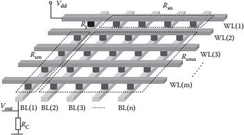
FIGURE 22.1 An illustration of an m × n crossbar array with a voltage-divider sensing scheme. The selected device is assumed to be at the upper left corner (Rj).
A voltage-divider sensing scheme is used here to read Rj. The selected WL (i.e., WL1) is biased to Vdd and the selected BL (i.e., BL1) is grounded through a reference resistor (RC). The state of Rj (i.e., LRS or HRS) is determined by reading the current flowing from Vdd (WL1) to ground (BL1) through Rj. This current is measured from the readout voltage (Vout) through RC. Rj in LRS (HRS) leads to high (low) current and high (low) Vout. If there were no sneak paths caused by unselected lines and devices, Rj and RC form a voltage divider and Vout is given by Vdd ⋅ RC/(Rj + RC). Therefore, RC can be optimized to enlarge the sensing margin ΔVout (i.e., Vout|Rj in LRS − Vout|Rj in HRS). It is straightforward to show that ΔVout maximizes at .
22.2.1 VOLTAGE CONFIGURATIONS FOR READING OPERATION
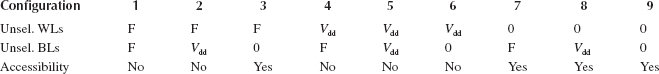
In reality, a large number of sneak paths exist owing to the unselected lines and devices. The bias schemes of the unselected WLs/BLs are important for the sensing margin during the reading operation. There are three bias options for the unselected WLs/BLs (Vdd, ground, or floating), which give nine possible voltage configurations for reading (Table 22.1). Notice that it is also possible to bias unselected WLs/BLs to a fraction of Vdd (partial bias), similar to the partial bias schemes used for the writing of crossbar arrays. However, as will be shown later, partial voltage schemes may not effectively improve the sensing margin, because they do not eliminate or reduce the parasitic leakage current through these sneak paths.
TABLE 22.1
Summary of Possible Voltage Configurations for the Reading Operation and the Crossbar Array Accessibility for Each Configuration
Source: A. Chen, The accessibility of nano-crossbar arrays of resistive switching devices, 11th IEEE Conference on Nanotechnology (IEEE-NANO), Portland, OR, pp. 1767–1771, © (2011) IEEE. With permission.
Note: Labels: “0”, grounded; “F”, floating.
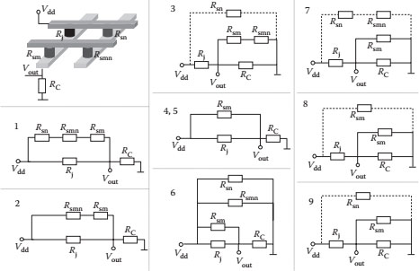
FIGURE 22.2 Equivalent circuits for the different reading voltage configurations.
For simplicity, it is also assumed that there is no parasitic access resistance from the voltage sources to the WLs and BLs. Therefore, these lines can be accurately biased to Vdd or ground. With the line resistance being ignored, the same voltage is passed along each WL and BL. Circuit symmetry allows unselected lines biased to the same voltage to be lumped together. As a result, large crossbar arrays can be simplified to simple 2 × 2 arrays with unselected devices lumped into equivalent resistances Rsn, Rsm, and Rsmn. Crossbar arrays with different voltage configurations can be converted to equivalent circuits shown in Figure 22.2 and solved analytically. These equivalent circuits also help to identify whether crossbar arrays can be accessed in each voltage configuration. Essentially, if leakage paths formed in parallel with Rj between Vdd and Vout (configurations 1, 2, 4–6), the state of Rj cannot be accurately identified because Vout is largely determined by the random resistance patterns of these parallel paths instead of Rj. In the other four voltage configurations (3 and 7–9), some unselected devices form parallel paths with the reference resistor RC between Vout and ground, which only affects the actual reference resistance. Vout is still mainly determined by Rj, that is, Vout’s for Rj = Ron and Rj = Roff can be distinguished, although it is no longer effective to optimize the sensing margin by choosing RC. Parallel leakage paths also form between Vdd and ground (dashed lines), which does not affect the sensing signals but reduces the power efficiency of the reading operation.
The last row of Table 22.1 summarizes the accessibility of each voltage configuration in reading operations.
In accessible voltage configurations (3 and 7–9), Vdd is divided between Rj and an effective reference resistor formed by RC and parallel resistors. The range of Vout and the sensing margin (ΔVout) can be derived analytically. Since Vout is higher when Rj is in LRS than when it is in HRS, Vout is equal to Vout(Rj = Ron) − Vout(Rj = Roff). For both Rj = Ron and Rj = Roff, Vout reaches the maximum (minimum) when unselected devices in parallel with RC are all in HRS (LRS). Let represent the minimum (maximum) value of Vout for Rj = Ron, and represent the minimum (maximum) value of Vout for Rj = Roff. These parameters are calculated as shown in Table 22.2. All these boundary values increase with rising RC and decrease with a larger array size. For large arrays (n, m → ∞), the different expressions in Table 22.2 for configuration 3 and configurations 7–9 converge to the same results. The worst-scenario sensing margin is given by the difference between and , defined as a normalized value of . Since is independent of the on/off ratio k and is lower for larger k, a higher on/off ratio helps to increase the sensing margin.
TABLE 22.2
Minimum and Maximum Values of Vout for Rj = Ron and Rj= Roff
Configuration 3 |
||||
Configurations 7–9 |
Source: A. Chen, The accessibility of nano-crossbar arrays of resistive switching devices, 11th IEEE Conference on Nanotechnology (IEEE-NANO), Portland, OR, pp. 1767–1771, © (2011) IEEE. With permission.
Note: rC = Rd/Ron; k = Roff/Ron; m and n are the WL and BL numbers.
Figure 22.3a plots the worst-scenario sensing margin as a function of RC (normalized to Ron) and array size for a square crossbar array (m = n) with the on/off ratio k = 10. This level of the on/off ratio is typical for resistive switching memory devices. The sensing margin decreases monotonically with the increase of array size from slightly above 10% (a 16-bit array of 4 × 4) to around 0.1% (a 64-kbit array of 256 × 256). This result shows that the sensing margin of crossbar arrays with linear resistive switching devices is very low even for kilobit arrays, which limits the feasible crossbar array size. To illustrate the RC effects, the dependence of sensing margin on RC is also plotted for 8 × 8 and 256 × 256 arrays in Figure 22.3b and c. There exists an optimal RC value for the maximum sensing margin. Both the optimal RC and the maximum sensing margin decrease with increasing array size.
22.2.3 DISTURBANCE AND POWER EFFICIENCY
In addition to the sensing margin, reading disturbance on unselected devices is another key performance measure. It can be seen from Figure 22.2 that the unselected devices along parallel leakage paths (dashed lines) are biased to Vdd during reading. Although Vdd for reading can be made low enough to not switch these devices, the voltage stress on the unselected devices may still degrade their reading endurance. Take configuration 3 as an example; the reading of Rj exposes all the half-selected devices connected in parallel in group Rsn to the reading voltage. If Rj is continuously read to the end of its reading endurance, all these devices in Rsn also experience similar reading stress. In configuration 7, Vdd is divided between Rsn and Rsmn along the parallel paths. However, Rsmn is much smaller than Rsn in large arrays, so devices in the Rsn group still experience the voltage stress close to Vdd. This constant exposure of unselected devices to voltage stress during reading operations may significantly accelerate the reading endurance failure of crossbar arrays.
The parallel leakage paths (dashed lines) also waste power, resulting in low power efficiency in the reading operation. Take configuration 9 as an example. In the worst case, Rj = Roff and unselected devices in group Rsn are all Ron. It can be shown that the power efficiency of the reading operation is lower than 1/[(n − 1)k], which is ~0.1% for a 100 × 100 array with an on/off ratio of 10. The best scenario for power efficiency arises when Rj = Ron and unselected devices in Rsn are all Roff. Calculation shows that the best power efficiency approaches k/(n − 1). With k = 10, the efficiency is still below 10% for arrays larger than 100 × 100. Therefore, most power is wasted during the reading of a crossbar array. The analysis above also shows that the on/off ratio may or may not help power efficiency, depending on the state of Rj and resistance patterns of the crossbar array. Power efficiency always decays with increasing array size because of more leakage paths.
FIGURE 22.3 (a) The worst-scenario sensing margin of a square crossbar array as a function of RC and array size (number of WLs/BLs) for voltage configurations 7–9; (b) and (c) show the dependence of the sensing margin on RC for 8 × 8 and 256 × 256 arrays. The on/off ratio k is assumed to be 10.
Leaving unselected WLs and BLs floating (configuration 1) may cause less disturbance and waste less power. This is because unselected devices are serially connected in each sneak path and therefore each of them is exposed to lower voltage in average. However, in the worst scenario, the state of Rj cannot be identified because of the sneak paths in parallel with it. Notice that the worst scenario for a sensing margin when unselected lines are floating is different from when they are grounded. Simply applying the same worst scenarios on different voltage configurations will lead to erroneous conclusions.
22.3 A CROSSBAR ARRAY SOLUTION BASED ON MATRIX ALGEBRA
The analysis above is based on simplified crossbar array equivalent circuits and analytical solutions. A general solution for crossbar arrays can be developed based on matrix algebra. The general solution provides detailed voltage/and current distribution in crossbar arrays and reading output voltage for any resistance patterns.
With the line resistance being ignored, the same voltage exists along each WL and BL. The WL voltages (VWL1,…, VWLm) and BL voltages (VBL1,…, VBLn) define the voltage distribution in crossbar arrays. Based on these (m + n) variables, all junction voltages, current distributions, and output voltage can be easily derived. For an array with a given resistance pattern {Rij} (1 ≤ i ≤ m, 1 ≤ j ≤ n), these unknown variables {VWLi, VBLj} can be solved based on matrix algebra. Table 22.3 shows the definition of the variables involved in the matrix-based solution. Access resistance is defined as the resistance between voltage sources and WLs/BLs. Notice that the analysis in the previous section ignored access resistance. An extremely high access resistance simulates floating lines. Kirchhoff’s law defines (m + n) equations for these unknown voltages and can be written in a matrix format as shown in Figure 22.4. All WL/BL voltages can be solved together from this matrix equation.
TABLE 22.3
Variables Used in the Matrix-Based Crossbar Array Solution
Variables |
Definitions |
WL and BL voltages |
|
Resistance at junction (i, j), that is, Ron or Roff |
|
Access resistance and applied voltage on the selected WL (row) |
|
Access resistance and applied voltage on the unselected WL (row) |
|
Access resistance and applied voltage on the selected BL (column) |
|
Access resistance and applied voltage on the unselected BL (column) |
The general solution can be applied on any resistance patterns. A large number of random resistance patterns can be generated to calculate the distribution of crossbar array parameters. Figure 22.5 shows an example of the calculated distributions of the readout voltage (Vout) for 1000 randomly generated resistance patterns for a 64 × 64 array. The gap between the Vout distributions for Rj in LRS and HRS represents the sensing margin. As shown in this figure, the sensing margin is only ~1%. It should be pointed out that for a (n × m) array, there are 2n × m possible resistance patterns because each junction has two possible resistance values (Ron or Roff). So even a small 8 × 8 array has >1019 (264) possible resistance patterns and it is impossible to simulate even a small portion of these possibilities. It has been shown that many of these resistance patterns are equivalent. Independent patterns of an (n × n) array are between nn and n2n [23]. This is significantly less than 2n × n possible patterns, but still a very large number. Therefore, for larger arrays, the simulation based on a small number of samples becomes less representative.
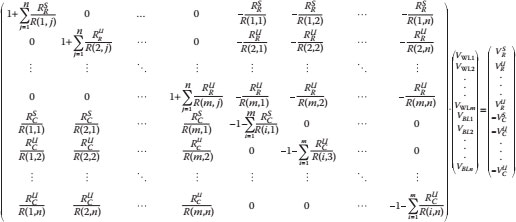
FIGURE 22.4 The matrix-based crossbar array equation with WL/BL voltages as unknown variables.
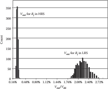
FIGURE 22.5 Distribution of readout voltage (Vout) for Rj in HRS and LRS based on 1000 random resistance patterns of a 64 × 64 crossbar array. The gap between these two distributions represents the sensing margin. It is assumed that the on/off ratio is 10, RC/Ron is 0.1, and access resistance is negligible (10−5 ⋅ Ron).
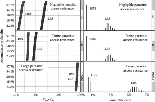
FIGURE 22.6 Left panels: accumulative probability of Vout for Rj in LRS and HRS; right panels: histogram of power efficiency of the reading operation. Three access resistance values are simulated: negligible (10−5 ⋅ Ron, top panels), finite (0.1 ⋅ Ron, middle panels), and large (105 ⋅ Ron, bottom panels).
Figure 22.6 shows the distributions of Vout normalized to Vdd (left panels) and power efficiency (right panels) calculated from this matrix-based statistical analysis. The top, middle, and bottom rows assume negligible access resistance (= 10−5 ⋅ Ron), finite access resistance (= 0.1 ⋅ Ron), and very highaccess resistance (105 ⋅ Ron), respectively. The top row is similar to the simplified analysis in Section 22.2 and the bottom row simulates floating unselected WLs and BLs. The results in Figure 22.6 indicate that the sensing margin (the gap between HRS and LRS Vout’s) decreases with increasing access resistance. Notice that floating unselected WLs/BLs helps to improve the power efficiency (especially for Rj in LRS); however, the sensing margin diminishes to 0. The power efficiency of reading an LRS device is higher than that of reading an HRS device, because a relatively higher percentage of current passes through LRS devices than HRS devices for the same unselected device resistance pattern. However, overall power efficiency is still very low because of the power wasted in the sneak paths.
22.4 EFFECT OF NONLINEAR MEMORY CHARACTERISTICS
Many RRAM devices demonstrate nonlinear I–V characteristics, which may improve the sensing margin. There are many forms of nonlinear I–V characteristics. Figure 22.7 shows a simple parabolic shape nonlinearity in I–V curves: both LRS and HRS can be described as I = a ⋅ V + b ⋅ V2, where a and b are constants with different values for LRS and HRS. A space–charge-limited conduction (SCLC) transport mechanism may give this type of I–V characteristics. Tunneling-based transport mechanisms (e.g., trap-assisted tunneling) may provide exponential I–V dependence and stronger nonlinearity. The nonlinearity ratio (ηLRS and ηHRS) here is defined as the ratio of the resistance at 0 V over that at Vdd. This ratio is defined for both LRS and HRS. Notice that different definitions of the nonlinearity ratio may be used in different papers, leading to different conclusions. By definition, the higher the nonlinearity ratio, the larger the changes of resistance over the operation voltage range. Nonlinearity in Figure 22.7 essentially describes the voltage-dependent resistance, that is, higher resistance at lower voltage. For nonlinear devices, the on/off ratio is also voltage dependent and should be defined at a certain voltage. If not specified, the on/off ratio of nonlinear devices discussed in this chapter is defined at Vdd.
To explain the nonlinearity effect, Figure 22.8 reconstructs the crossbar array in Figure 22.1 to highlight the composition of sneak paths. R(i,j) at junction (i,j) is the selected device. WLi is biased to Vdd and BLj is biased to ground through RC. Unselected WLs/BLs are assumed to be floating. For the current to flow from WLi to BLj, it can go directly through R(i,j) (the selected path) or through parallel leakage paths formed by three unselected devices (sneak paths). Current direction along any sneak path is always a combination of WL-to-BL, BL-to-WL, and WL-to-BL; therefore, one of the three unselected devices is always reverse biased along any sneak path. This explains why rectifying devices (e.g., diode) can improve the accessibility of crossbar arrays because their high reverse resistance reduces the leakage through sneak paths. Notice that the voltage drop between WLi and BLj is divided by the three unselected devices along any sneak path, that is, voltage of these unselected devices is relatively smaller than the voltage on the selected device. Therefore, the nonlinearity-induced resistance increase is more prominent on unselected devices than on the selected device. This also helps to reduce the leakage through sneak paths and improve the sensing margin.
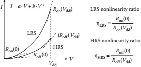
FIGURE 22.7 An illustration of nonlinear I–V characteristics and the definition of nonlinearity ratio.
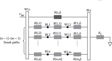
FIGURE 22.8 Reconstruct a crossbar array to highlight the composition of sneak paths.
To quantify the nonlinearity effect on the sensing margin, let us use configuration 9 in Figure 22.2 (unselected WLs and BLs are all grounded) as an example. The worst-scenario sensing margin . The minimum Vout for Rj = Ron (i.e., ) arises when unselected devices in the Rsm group are all in LRS, that is, Rsm = Ron/(m − 1). Because the voltage on Rj and Rsm is below Vdd, both Rj and Rsm increase from their values at Vdd when Vout < Vdd/2, V(Rj) is larger than V(Rsm) and therefore Rj increases less than Rsm, which helps to increase and the sensing margin. Similarly, nonlinearity in HRS also increases , which, however, reduces the sensing margin. Therefore, the change in the sensing margin depends on the nonlinearity ratios of LRS and HRS.
Figure 22.9 shows the calculated sensing margin for a 64-kbit array (256 × 256) as a function of the nonlinearity ratios of LRS and HRS. As expected, the sensing margin increases with the LRS nonlinearity, but decreases with the HRS nonlinearity. With appropriate nonlinearity ratios in LRS and HRS, sensing margin close to 5% can be achieved in a 256 × 256 array, significantly better than the sensing margin of <0.2% for linear devices.
Figure 22.10 shows the calculated worst-scenario sensing margin as a function of RC and array size for nonlinear devices with ηLRS = 100 and ηHRS = 1. The overall shape is very similar to Figure 22.3 for linear devices; however, the sensing margin is significantly higher. Figure 22.10b and c plots the sensing margin dependence on RC for two example array sizes. At optimal RC, the maximum sensing margin is ~25% for a small 8 × 8 array and is slightly below 5% for a 256 × 256 array. It is expected that stronger nonlinearity (e.g., exponential I–V characteristics) may improve the sensing margin even more and enable larger crossbar array sizes.
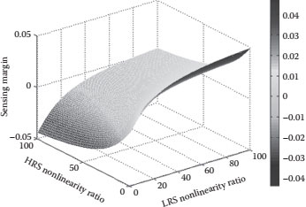
FIGURE 22.9 Worst-scenario sensing margin versus LRS and HRS nonlinearity ratios for a 256 × 256 array with an on/off ratio of 10 defined at Vdd.
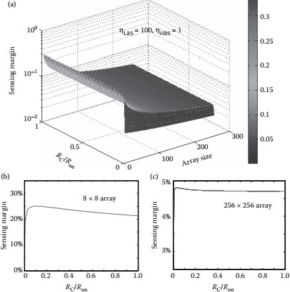
FIGURE 22.10 (a) The worst-scenario sensing margin of a square crossbar array with nonlinear RRAM devices as a function of RC and array size; (b) and (c) show the dependence of the sensing margin on RC for 8 × 8 and 256 × 256 arrays.
The matrix-based method in Section 22.3 can also be used to simulate the statistical distribution of crossbar arrays of a nonlinear device. Figure 22.11 compares the calculated Vout distributions for linear and nonlinear devices in a 64 × 64 array. The sensing margin increases significantly owing to the nonlinearity in the memory device characteristics.
22.5 WRITING OPERATION OF CROSSBAR ARRAYS
The writing operation of crossbar arrays has different requirements from the reading operation. Sufficiently high voltage and current need to be delivered to the selected device and, at the same time, disturbance on unselected devices needs to be minimized. The parasitic leakage paths affect the switching operation by degrading the voltage delivery to the selected device and reducing power efficiency. The WL and BL resistance is important for the writing operation because line resistance degrades the voltage delivery along the lines. Since many leakage paths exist along a line, to drive a certain level of current to the end of a line, significantly higher current may be required at the beginning of a line. This high current requirement may cause reliability concerns.
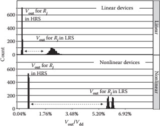
FIGURE 22.11 Compare the readout voltage distribution of 64 × 64 crossbar arrays with linear and nonlinear devices, showing the improvement of the sensing margin owing to nonlinearity. The nonlinearity ratios are assumed to be ηLRS = 100 and ηHRS = 1.
Resistive switching devices can be unipolar (set and reset happen in the same voltage polarity direction) or bipolar (set and reset in the opposite directions). The switching operation of a crossbar array of bipolar switching devices is more complicated than that of unipolar devices, because the reversal of the switching voltage may have different effects on the selected device depending on its location inside of the array. Select devices can help to improve the writing operation, but it is challenging to develop functional select devices for bipolar switching devices. Two terminal devices that provide both two-direction conduction and rectifying characteristics are difficult to find.
During the writing operation, the selected WL is biased to Vdd and the selected BL is grounded. Two partial bias schemes are commonly used for the unselected WLs/BLs: (1) the “1/2 bias scheme” and (2) the “1/3 bias scheme.” In the “1/2 bias scheme,” all unselected WLs and BLs are biased to Vdd/2. If all line resistance and access resistance are ignored, unselected devices in the Rsmn group are zero biased and unselected devices in the Rsm and Rsn groups are all biased to Vdd/2. In the “1/3 bias scheme,” the unselected WLs and BLs are biased to Vdd/3 and 2Vdd/3, respectively. As a result, all the unselected devices are biased to either +Vdd/3 or −Vdd/3. Figure 22.12 illustrates these two bias schemes and the junction voltages. Therefore, the “1/2 bias scheme” minimizes the number of biased unselected devices because most unselected devices (group Rsmn) are zero biased. However, the half-selected devices may experience up to Vdd/2 voltage disturbance. The “1/3 bias scheme” minimizes the maximum voltage disturbance because the maximum voltage on unselected devices is Vdd/3. However, all the unselected devices are exposed to a certain voltage bias. So the “1/2 bias scheme” is preferred for leakage reduction and the “1/3 bias scheme” is favored for disturbance minimization.
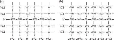
FIGURE 22.12 Partial bias schemes for the writing of crossbar arrays: (a) 1/2 bias scheme; (b) 1/3 bias scheme. The values at the junction points are the voltage drop at the junctions.
The voltage distribution during the writing operation can also be solved using the same matrix algebra in Section 22.3. Figure 22.13 shows the distribution of the selected device voltage and the maximum voltage on unselected devices, based on the randomly generated resistance patterns in crossbar arrays. The “1/2 bias scheme” is used in this calculation. Two levels of access resistance (10−5 ⋅ Ron and 10−2 ⋅ Ron) are simulated and two array sizes are considered, 256 × 256 (on the left) and 64 × 64 (on the right). With negligible access resistance, Vdd is accurately delivered to the selected device and maximum disturbance voltage on unselected devices is Vdd/2. Both distributions focused narrowly on these values. These results do not change with the increase of array size. With finite access resistance, the voltage delivered to the selected device degrades significantly from the Vdd by more than 50% in large arrays. To compensate for this degradation, higher external voltage needs to be applied to ensure the switching of a selected device; however, this also increases the change of disturbance on unselected devices. Although the maximum disturbance voltage is also decreasing, the gap between the selected device voltage and the maximum disturbance voltage on unselected devices decreases in large arrays. Both distributions also show finite slope, indicating increasing dependence of voltage distributions on the resistance patterns of the crossbar array.
The simulation in Figure 22.13 only considered the effects of access resistance and still neglected the line resistance; therefore, the same voltage is passed along all the lines no matter how large the array is. Line resistance has an important impact on the writing operation because the resistanceinduced voltage degradation may cause large variation on device voltages at the beginning and the end of the lines. This issue is more prominent for crossbar arrays of resistive switching devices owing to the high writing voltage and leakage in the arrays. In comparison, flash memory arrays have a much lower writing current (owing to the tunneling-based writing mechanism) and lower leakage (owing to the transistors as select devices). Figure 22.14 calculated the voltage decay along an access line up to 512 devices along the line for different line resistance RL (defined as the resistance between two neighboring devices). Assuming a Cu-interconnect and resistivity of 3.5 μΩ cm at the 22 nm technology node [21], an interconnect line aspect ratio of 2 will give RL~1–2 Ω. For resistive switching memories with Ron of 10–100 kΩ, this corresponds to RL/Ron between 10−4 and 10−5 in the figure. The voltage passing along the line may decay by 20%–50% just after 100 devices. This voltage degradation may constrain realistic crossbar arrays to a relative small size. Select devices can help to reduce array leakage and voltage degradation, which may enable a larger array size. Nonlinear device characteristics have similar effects. However, it is still a great challenge and may be impossible to build crossbar array at the size similar to flash memories, because of the intrinsically higher leakage and writing current. This issue becomes more critical for highly scaled devices, because both array leakage current and line resistance increases when device size scales down.
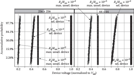
FIGURE 22.13 Calculated distribution of the selected device voltage and the maximum voltage of unselected devices for the “1/2 bias” scheme. Two different access resistance Ra (= 10−5Ron or 10−2Ron) and two different array sizes (256 × 256 and 64 × 64) are simulated.
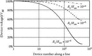
FIGURE 22.14 Calculated voltage decay along a line for different line resistance (RL) of 10−6, 10−5, and 10−4 (normalized to Ron).
Another important issue rarely discussed for the writing operation of crossbar arrays is the current delivery. Resistive switching memories usually require 10–100 μA or even a higher switching current [24]. Calculation shows that even for a small 1 k (32 × 32) array with RL/Ron of 10−4, the current delivered to the end of a line may be as small as 2% of the initial value from the power sources. This is due to the large amount of sneak paths that diverge the current while it travels along a line. This inefficient current delivery in crossbar arrays requires much higher current from voltage sources, presenting both design and reliability challenges. Resistive switching devices with low-switching current (e.g., sub-1 μA operation) have been demonstrated; however, the reliable operation of these devices with array statistics is still lacking [25]. Similar to the switching voltage, the current degradation also limits a realistic crossbar array size and imposes stringent requirements on memory device characteristics.
Crossbar memory arrays have a broad range of applications in nanoelectronics. Baseline analysis in this chapter shows that sneak paths and sensing margin degradation limit practical crossbar memory array size. With the linear resistive switching memory devices, it is expected that the crossbar array size is limited to below several kilobits. Nonlinearity in memory device characteristics can help to reduce leakage through sneak paths and may enable crossbar array size up to several hundred kilobits. However, stable and repeatable resistive switching memory devices with sufficiently strong nonlinearity are still under research. Voltage and current delivery requirements during writing operations impose more constraints on crossbar array size. Line resistance needs to be considered in realistic analysis of crossbar array switching operations because of the resistanceinduced voltage and current degradation. Owing to these constraints, it is impractical for crossbar arrays to compete with flash-based memory arrays in terms of array size. However, small crossbar arrays can be combined with transistor access devices where each small crossbar array is addressed by one transistor. The array size needs to be chosen appropriately to optimize both operation performance and array efficiency.
Emerging oxide-based resistive switching devices are still facing severe challenges, among which variability is considered an intrinsic limitation owing to the stochastic switching mechanisms. In a transistor-based memory array, the isolation provided by transistors can help to minimize the effect of each device on the overall array operation. However, in crossbar arrays without such isolation components, the variability of each device is well reflected in the overall array performance. The sensing margin may shrink owing to the spreading of the readout voltage distribution. The writing operation may be affected by the unpredicted voltage/current variation owing to the device instability. Although nonlinear memory devices are considered a promising solution for self-selecting crossbar arrays without select devices, large variability may also exist in nonlinear resistive switching devices and limit crossbar array designs.
Two-terminal select devices are ultimately required to build functional crossbar arrays. Select devices need to not only isolate devices but also allow sufficient voltage and current to be passed to devices. Diodes with rectifying characteristics are considered a promising solution; however, diodes with a high rectifying ratio and drive current are difficult to find. Contact resistance is an important practical limitation on the diode drive current, which becomes an even bigger challenge when devices scale down. In addition, diodes usually work only for unipolar switching devices. Some volatile switching devices have also been considered for select devices in crossbar arrays [26]; however, their feasibility has not been fully proven either.
In summary, crossbar memory arrays provide promising opportunities for nanoelectronics. Their high density and low cost may enable unprecedented applications. To realize these potential opportunities, many challenges in the sensing and writing of crossbar arrays still need to be addressed by both device innovation and creative circuit designs.
1. N.Z. Haron and S. Hamdioui, Emerging crossbar-based hybrid nanoarchitectures for future computing systems, International Conference on Signals, Circuits and Systems, Nabeul, Tunisia, 2008.
2. S.C. Goldstein et al., Nanofabrics: Spatial computing using molecular electronics, Proceedings of the 28th Annual International Symposium on Computer Architecture (ISCA’01), Gothenburg, Sweden, 2001, pp. 178–191.
3. A. DeHon, Array-based architecture for FET-based nanoscale electronics, IEEE Transactions on Nanotechnology, 2, 2003, 23–32.
4. T. Wang et al., Opportunities and challenges in application-tuned circuits and architecture based on nanodevices, First ACM Conference on Computer Frontier, Ischia, Italy, 2004, pp. 503–511.
5. K.K. Likharev, et al., Afterlife for silicon: CMOL circuit architectures, Proceedings of 2005 5th IEEE Conference on Nanotechnology, 2005, 175–178.
6. G.S. Sinder and R.S. Williams, Nano/CMOS architecture using a field-programmable nanowire interconnect, Nanotechnology 18, 2007, 1–11.
7. Y. Chen, et al, Nanoscale molecular-switch crossbar circuits, Nanotechnology 14, 2003, 462–468.
8. M.M. Ziegler and M.R. Stan, Design and analysis of crossbar circuits for molecular nanoelectronics, Proceedings of the 2002 2nd IEEE Conference on Nanotechnology, Arlington, VA, 2002, pp. 323–327.
9. G.S. Rose et al., Design approaches for hybrid CMOS/molecular memory based on experimental device data, Proceedings of the 16th ACM Great Lakes Symposium on VLSI, Philadelphia, PA, 2006, pp. 2–7.
10. M.R. Stan, et al, Molecular electronics: From devices and interconnect to circuits and architecture, Proc. IEEE 91, 2003, 1940–1957.
11. W. Liu and C.M. Lieber, Nanoelectronics from the bottom up, Nature Mater. 6, 2007, 841–850.
12. Emerging Research Devices, International Technology Roadmap of Semiconductors (ITRS) report, 2011.
13. M. Crowley, et al, 512Mb PROM with 8 layers of antifuse/diode cells, IEEE International Solid-State Circuits Conference, 2003, 16.4.
14. C.J. Chevallier, et al, A 0.13 μm 64 Mb multi-layered conductive metal-oxide memory, IEEE International Solid-State Circuits Conference, 2010, 14.3.
15. Y. C. Chen, et al, An access-transistor-free (0T/lR) non-volatile resistance random access memory (RRAM) using a novel threshold switching, self-rectifying, IEDM Tech. Dig., 2003, pp. 905–908.
16. D. Kau, et al, A stackable cross point phase change memory, IEDM Tech. Dig., 2009, pp. 617–620.
17. Y. Sasago, et al, Cross-point phase change memory with 4F2 cell size driven by low-contact-resistivity poly-Si diode, Symposium on VLSI Technology, 2009, pp. 24–25.
18. A. Flocke and T. G. Noll, Fundamental analysis of resistive nano-crossbars for the use in hybrid nano/CMOS-memory, 33rd European Solid-State Circuits Conference, Munich, 2007, pp. 328–331.
19. A. Flocke et al., A fundamental analysis of nano-crossbars with non-linear switching materials and its impact on TiO2 as a resistive layer, 8th IEEE Conference on Nanotechnology, Arlington, TX, 2008, pp. 319–322.
20. G. Csaba and P. Luigi, Read-out design rules for molecular crossbar architectures, IEEE Trans. Nanotech. 9, 2009, 369–374.
21. E. Linn, R. Rosezin, C. Kügeler, and R. Waser, Complementary resistive switches for passive nanocrossbar memories, Nat. Mater. 9, 2010, 403–406.
22. A. Chen, The accessibility of nano-crossbar arrays of resistive switching devices, 11th IEEE Conference on Nanotechnology (IEEE-NANO), Portland, OR, 2011, pp. 1767–1771.
23. P.P. Sotiriadis, Information storage capacity of crossbar switching networks, Proceedings of the 13th ACM Great Lakes Symposium on VLSI, Washington, DC, 2003, pp. 45–49.
24. A. Chen, et al, Non-volatile resistive switching for advanced memory applications, International Electron Device Meeting (IEDM) Technical Digest, 2005, pp. 765–768.
25. C.H. Cheng, A. Chin, and F. S. Yeh, Ultralow switching energy Ni/GeOx/HfON/TaN RRAM, IEEE Electron. Lett. 32, 2011, 366–368.
26. M.J. Lee, et al, Two series oxide resistors applicable to high speed and high density nonvolatile memory, Adv. Mater. 19, 2007, 3919–3923.