
CONTENTS
23.1 Introduction
23.2 Basic Simulation Models
23.3 Memristive Models
23.3.1 Linear Memristive Model
23.3.2 Non-Linear Memristive Model
23.4 Conclusion
References
Resistive switches [1] are two-terminal devices that offer a nonvolatile switching behavior when applying voltage pulses. Although individual devices have a low-power requirement [2], passive crossbar arrays show significant power losses due to parasitic current sneak paths [3]. This so-called “sneak-path problem” does not only lead to increased power consumption, but it also complicates or even prevents proper array read operations. In Figure 23.1, a section of a passive crossbar array is depicted, illustrating the read operation of the lower left element. In case 1, the element is considered to be in the high-resistive state (HRS), while in case 2 the element is considered to be in the low-resistive state (LRS). Since neighboring cells are low resistive in both cases, the read currents are large in both cases, making a proper reading difficult. To solve this problem, the implementation of a rectifying diode-like selection device was suggested so far [4]. However, this approach is difficult to realize for bipolar resistive switches, since high current densities are required. In an alternative approach, antiserially connected bipolar resistive switches are applied to form a complementary resistive switch (CRS) [5,6]. Complementary resistive switches alleviate size limitations for passive crossbar array memory devices by the elimination of sneak paths because of high-resistive storing states. In Figure 23.2, the basic behavior of a CRS cell is illustrated. If, for example, element B is in the LRS and element A is in the HRS, almost all voltage drops at element A until Vth,1 is reached. At this point (A), element A switches to the LRS and element B remains in the LRS, because the potential drop at A is far below Vth,RESET. The CRS state is defined as “ON” with both elements how being low resistive and having an equal voltage drop. If the voltage reaches Vth,2(B), element B becomes high resistive, because this is equivalent to a voltage drop of Vth,RESET at element B. This state is defined as “0.” For all applied voltages larger than Vth,3, element B stays high resistive and element A low resistive. If a potential V comes into the range Vth,4 < V < Vth,3(C), the high-resistive element B switches to the LRS and both elements in the CRS are in the LRS (state “ON”). If the negative potential exceeds Vth,4, element A switches back to HRS (D) and the resulting state is “1.” In Table 23.1, the CRS states are depicted. The “OFF” state is only found in uninitialized cells and is not considered further in the following. The states “0” and “1” are the logical storage states and the state “ON” occurs only on a reading of the memory state. The internal memory states “0” and “1” of a CRS cell are indistinguishable at low voltages because state “0” as well as state “1” show a high resistance. Therefore, no parasitic current paths, which can only be induced by low-resistive cells in the crossbar, can arise. To read the stored information (“0” or “1”) of a single CRS cell, a read voltage must be applied to the CRS cell. If the CRS cell is in state “1,” the cell switches to the “ON,” state and if the cell is in state “0,” the cell remains in state “0.” By this selective switching to the “ON,” state, the stored information is destroyed (destructive read). An alternative destructive read approach uses a voltage V > Vth,2 resulting in a current spike when HRS/LRS applies while no current spike occurs for LRS/HRS. In ref. [7], this mode is used for logic applications. Note that for a destructive readout, it is necessary to write back the previous state of the cell after the reading. This requirement is not present when using a nondestructive readout scheme as proposed in ref. [8]. In general, the writing of state “1” requires a negative voltage (V < Vth, 4), and for writing a “0” a positive voltage V > Vth, 2 is required.
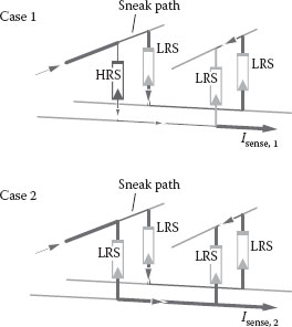
FIGURE 23.1 Sneak-path problem in passive crossbar arrays.
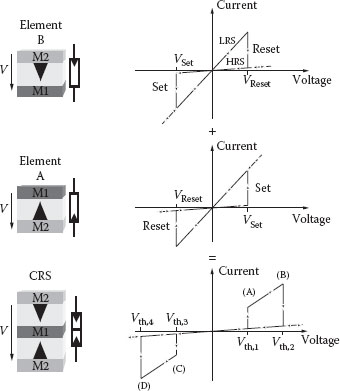
FIGURE 23.2 A complementary resistive switch results from the antiserial connection of two elements A and B. For example, M1 is Cu and M2 is Pt.
CRS |
Element A |
Element B |
Overall Resistance |
0 |
HRS |
LRS |
≈ HRS |
1 |
LRS |
HRS |
≈ HRS |
ON |
LRS |
LRS |
LRS + LRS |
OFF |
HRS |
HRS |
>> HRS; only initial state |
Since the CRS cells consist of two antiserially connected bipolar resistive elements, for example, electrochemical metallization (ECM) elements [1], it is straightforward to use their corresponding compact simulation models for circuit simulation. First, a basic model (using a fixed threshold voltage) is applied. In the next step, dynamical models (the so-called memristive models [9,10]) are applied.
In Figure 23.3a, a simulation of a bipolar resistive switch is depicted when applying a triangular voltage sweep. Fixed set and reset voltages are assumed. The corresponding simulation of two antiserially connected elements is depicted in Figure 23.3b. From this simulation result, the basic functionality of CRS can be understood in detail. Initially, element A is high resistive (HRS) and element B is low resistive (LRS), which corresponds to the HRS/LRS state. At Vth,1(A), element A switches, resulting in LRS/LRS. If the voltage exceeds Vth,2, the cell switches to LRS/HRS (B). For voltages smaller than Vth,3 the element B switches to LRS, and hence the cell is again in the LRS/LRS state (C). When the voltage exceeds Vth,4, the cell switches back to HRS/LRS (D). To read the device, a voltage in the range Vth,1 < V < Vth,2 is applied, which switches the cell to LRS/LRS if the previous state was HRS/LRS (read a “1”). If the previous state was LRS/HRS, the CRS cell does not switch and stays in the HRS (read a “0”). After a readout, a write-back step is performed.
To simulate a large memory or logic structures along with the CMOS periphery, more realistic dynamical compact circuit models are needed. While these models should be as simple as possible, they have to provide the correct input–output behavior. Since bipolar resistive switches show a pinched hysteresis loop, they can be considered as memristive systems or memristors [9, 10 and 11]. A memristive system is a special case of a dynamical system and is defined by a state equation (23.1) and a readout equation (23.2):
(23.1) |
(23.2) |
u is the current I and y the voltage V, or vice versa, while x is the inner state variable which is multidimensional in general. For u = I, h is the resistance R, whereas h is the conductance G for u = V. h(x,0) ≠ ∞ must hold to result in a pinched hysteresis loop [10]. Additionally, for a nonvolatile memory device, f(x,u) = 0 for u = 0 must hold, since no change of state should occur without external excitation. For modeling resistive switches as memristive systems, it is crucial to identify the inner state variables. At least one state variable describing a structural change is needed, for example, the length of a filament in electrochemical metallization cells (ECM) [13].
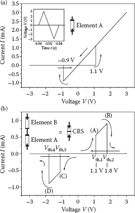
FIGURE 23.3 Spice simulation of a resistive switch (a) and CRS cell (b) with fixed threshold voltages. (From E. Linn et al., Modeling complementary resistive switches by nonlinear memristive system, Proceedings of the 11th IEEE Conference on Nanotechnology, Portland, OR, pp. 1474–1478, © (2011) IEEE. With permission.)
23.3.1 LINEAR MEMRISTIVE MODEL
Several models in the literature are based on the basic memristive approach by the HP group [11]. Here, an adapted model implementation from ref. [14] for a memristive element A (Figure 23.4a) is applied. In this model, σ(•) is the step function, wA is the state variable which corresponds to the filament length in an ECM device, d is the thickness of the active layer, C1 is a fitting constant, RLRS is the low resistance value, and RHRS is the high resistance value:
(23.3) |
(23.4) |
(23.5) |
In Equation 23.3, there is a range limitation, allowing only filament lengths in the range of 0 < wA < d. After reaching the range limit, the state change is set to zero until the current polarity changes. Within the range 0 < wA < d, Equation 23.3 reduces to
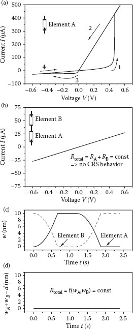
FIGURE 23.4 Spice simulation for linear model. (From E. Linn et al., Modeling complementary resistive switches by nonlinear memristive system, Proceedings of the 11th IEEE Conference on Nanotechnology, Portland, OR, pp. 1474–1478, © (2011) IEEE. With permission.)
(23.6) |
For an element B, index A is replaced by B in Equations 23.3 through 23.6. If we consider two memristive elements A and B connected antiserially (which means IB = −IA) and with initial values wA(t = 0) = 0 and wB(t = 0) = d, which corresponds to HRS/LRS, we obtain an I–V characteristic not showing any CRS behavior (cf. Figures 23.4b and 23.3b). This is a direct consequence of the linear dependency of R on the state variable w and the fact that is an odd function of the input current I. This can be seen when calculating the total resistance of the CRS cell
(23.7) |
for the given system
(23.8) |
(23.9) |
By integration of Equation 23.8 and the use of initial conditions, we can calculate
(23.10) |
Since wA and wB even up (Figure 23.4c,d), a constant total resistance Rtotal (Equation 23.7) results from Equations 23.9 and 23.10:
(23.11) |
Since the total resistance is constant, no CRS behavior can result from such a linear memristive model. The equations modeling a single element (Equations 23.8 and 23.9) can also be transformed to a second-order linear system:
(23.12) |
(23.13) |
(23.14) |
Thus, such a linear memristive model does not provide correct simulation results for CRS cells. Subsequently, this model is too simple to render correct bipolar resistive switch behavior.
23.3.2 NON-LINEAR MEMRISTIVE MODEL
To overcome the limitation of the linear model, a nonlinear model must be implemented. Here, an electron-transfer mechanism at the interfaces is assumed which is described by the Butler–Volmer equation. This was simulated in ref. [15]. Figure 23.5a shows the applied equivalent circuit. The main circuit consists of a voltage source, the memristive element A, and a series resistor. An auxiliary circuit is used for a state variable calculation with and Vw = wA implementing the same range limitation 0 < wA < d as for the linear model (Figure 23.5a, right). The initial memristive model (Figure 23.5b) includes two paths, one for the ionic Iion and the other for the electronic current Iel. In this model implementation, Iel ≫ Iion holds for the whole voltage range considered. Since we assume two identical interfaces, both interfaces can be described by one current source (Iion in Figure 23.5b) using the Butler–Volmer equation [15,16]. This results in
(23.15) |
In the gap between a filament and an electrode, the ionic resistance and the electronic resistance are given as
(23.16) |
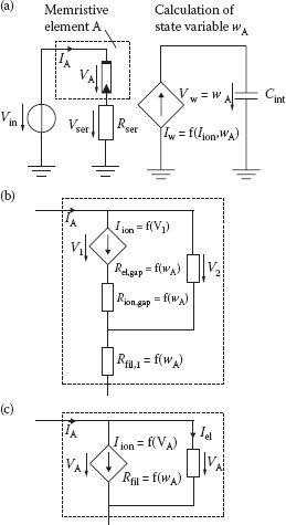
FIGURE 23.5 Memristive model of an ECM element based on an electron-transfer mechanism. (From E. Linn et al., Modeling complementary resistive switches by nonlinear memristive system, Proceedings of the 11th IEEE Conference on Nanotechnology, Portland, OR, pp. 1474–1478, © (2011) IEEE. With permission.)
and
(23.17) |
respectively.
Both resistances are dependent on the state variable wA, as is the resistance of the filament
(23.18) |
To satisfy Equation 23.2, the current IA must be an explicit function of VA and wA. This is not the case for the initial model in Figure 23.5b, since there are implicit dependencies:
(23.19) |
By making two simplifications, an explicit formulation as a memristive system is possible. The first one concerns the ionic current Iion, which can be defined only by the Butler–Volmer equation, neglecting the small voltage drop at the ionic resistance of the gap Rion,gap. Note that for larger voltages Vin, this resistance must be considered. The second simplification is also related to the ionic current Iion, which is small compared to the electronic current Iel, and thus the voltage drop of the ionic current at the filament (Rfil,1) is neglected as well. This simplification is valid for the small-to-moderate voltages which are considered in this work. The corresponding circuit model is depicted in Figure 23.5c. The resistance Rfil is the sum of Rfil,1 and Rel,gap, which is equivalent to Equation 23.9:
(23.20) |
Rfil,0 (=1 kΩ) is the minimum filament resistance value and Rfil,max (=1 MΩ) is the maximum filament resistance value. Owing to the applied simplifications, V1 = VA and V2 = VA result, leading to the final memristive system (Figure 23.5c)
(23.21) |
(23.22) |
This system is in accordance with Equations 23.1 and 23.2 and satisfies f(wA,VA) = 0 for VA = 0, since sinh(0) = 0. Because sinh(0)/0 = 1 also, G(wA,0) ≠ ∞ holds. Note that the change of the state variable (Equation 23.21) is controlled by the ionic current and the readout current (Equation 23.22) is dominated by the electronic current. Figure 23.6 shows the simulation results. In Figure 23.6a, a typical I–V characteristic of element A and a series resistor Rser is shown. If we now consider two memristive elements A and B connected antiserially, we observe a CRS behavior (Figure 23.6b). This I–V characteristic is similar to the characteristic shown in Figure 23.3b. The characteristics of the inner state variables wA and wB, which correspond to the filament length in each element, are shown in Figure 23.6c. In contrast to the linear model, the state variables of the elements A and B do not even up for the nonlinear model (Figure 23.6d).
The different dynamic can be understood by having a closer look at the voltage divider which applies for the CRS. First, almost all voltage drops at element A, which is in HRS. Since a state change is a nonlinear function of VA, the filament growth velocity increases with applied voltage Vin. When the filament reaches the counter electrode (wA = d), element A switches to LRS. Now, both elements A and B are in the LRS, taking an equal voltage drop which may additionally be reduced by a series resistor. With a further increase of the applied voltage Vin, the voltage VB becomes large enough to induce a fast decrease of the filament, thus switching element B to HRS. The influence of a series resistor on the I–V characteristics of single elements as well as CRS cells is shown in Figure 23.7. For small Rser, the very asymmetric I–V characteristic of an ECM element (Figure 23.7a) only results in a current spike in the CRS configuration (Figure 23.7b). For larger Rser, a stable LRS/LRS state is obtained for the CRS cells built of asymmetric ECM cells, as stated in ref. [5].
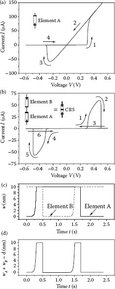
FIGURE 23.6 Spice simulation for nonlinear model. (From E. Linn et al., Modeling complementary resistive switches by nonlinear memristive system, Proceedings of the 11th IEEE Conference on Nanotechnology, Portland, OR, pp. 1474–1478, © (2011) IEEE. With permission.)
For realistic simulations, physics-based nonlinear memristive models must be applied. By applying a physics-based nonlinear model for ECM elements, it is possible to simulate the correct CRS behavior for antiserially combined elements. However, the results show that it is not feasible to model a CRS cell by two antiserially connected linear current-controlled memristive elements. Therefore, simple linear memristive models, which are often used in the literature, are inapplicable for simulation. Since CRS behavior should result for all bipolar resistive switches connected antiserially, the occurrence of CRS behavior is a good indicator for model consistency.
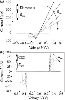
FIGURE 23.7 Variation of series resistance for a resistive switch (a) and CRS (b), simulated with the phys-ical-based model from Figure 23.5. (From E. Linn et al., Modeling complementary resistive switches by nonlinear memristive system, Proceedings of the 11th IEEE Conference on Nanotechnology, Portland, OR, pp. 1474–1478, © (2011) IEEE. With permission.)
1. R. Waser, S. Menzel, and R. Bruchhaus, Nanoelectronics and Information Technology (3rd edition), Wiley-VCH, Weinheim, Germany, 2012.
2. V. V. Zhirnov, R. Meade, R. K. Cavin, and G. Sandhu, Scaling limits of resistive memories, Nanotechnology, 22, 254027/1–21, 2011.
3. A. Flocke and T. G. Noll, Fundamental analysis of resistive nano-crossbars for the use in hybrid Nano/CMOS-memory, Proceedings of the 33rd European Solid-State Circuits Conference, Munich, Germany, 2007, pp. 328–331.
4. J.-J. Huang, Y. -M. Tseng, C.-W. Hsu, and T.-H. Hou, Bipolar nonlinear Ni/TiO2/Ni selector for 1S1R crossbar array applications, IEEE Electron Device Lett., 32, 1427–1429, 2011.
5. E. Linn, R. Rosezin, C. Kügeler, and R. Waser, Complementary resistive switches for passive nanocrossbar memories, Nat. Mater., 9, 403–406, 2010.
6. R. Rosezin, E. Linn, L. Nielen, C. Kügeler, R. Bruchhaus, and R. Waser, Integrated complementary resistive switches for passive high-density nanocrossbar arrays, IEEE Electron Device Lett., 32, 191–193, 2011.
7. R. Rosezin, E. Linn, C. Kügeler, R. Bruchhaus, and R. Waser, Crossbar logic using bipolar and complementary resistive switches, IEEE Electron Device Lett., 32, 710–712, 2011.
8. S. Tappertzhofen, E. Linn, L. Nielen, R. Rosezin, F. Lentz, R. Bruchhaus, I. Valov, U. Böttger, and R. Waser, Capacity based nondestructive readout for complementary resistive switches, Nanotechnology, 22, 395203/1–7, 2011.
9. L.O. Chua and S.M. Kang, Memristive devices and systems, Proc. IEEE, 64, 209–223, 1976.
10. L.O. Chua, Resistance switching memories are memristors, Appl. Phys. A-Mater. Sci. Process., 102, 765–783, 2011.
11. D. B. Strukov, G. S. Snider, D. R. Stewart, and R. S. Williams, The missing memristor found, Nature, 453, 80–83, 2008.
12. E. Linn, S. Menzel, R. Rosezin, U. Böttger, R. Bruchhaus, and R. Waser, Modeling complementary resistive switches by nonlinear memristive system, Proceedings of the 11th IEEE Conference on Nanotechnology, Portland, OR, 2011, pp. 1474–1478.
13. I. Valov, R. Waser, J. R. Jameson, and M. N. Kozicki, Electrochemical metallization memories—Fundamentals, applications, prospects, Nanotechnology, 22, 254003/1–22, 2011.
14. S. Shin, K. Kim, and S. M. Kang, Compact models for memristors based on charge-flux constitutive relationships, IEEE Trans. Comput-Aided Des. Integr. Circuits Sys., 29, 590–598, 2010.
15. S. Menzel, B. Klopstra, C. Kügeler, U. Böttger, G. Staikov, and R. Waser, A simulation model of resistive switching in electrochemical metallization memory cells, Mater. Res. Soc. Symp. Proc., 1160, 101–106, 2009.
16. S. Menzel, U. Böttger, and R. Waser, Simulation of multilevel switching in electrochemical metallization memory cells, J. Appl. Phys., 111, 014501, 2012.