
Hybrid Design of a Memory Cell Using a Memristor and Ambipolar Transistors |
CONTENTS
24.1 Introduction
24.2 Memristor
24.3 Ambipolar Transistor
24.4 Proposed Memory Cell
24.4.1 WRITE Operation
24.4.1.1 WRITE a “1”
24.4.1.2 WRITE a “0”
24.4.2 READ Operation
24.5 Simulation Results
24.5.1 WRITE Operation
24.5.2 READ Operation
24.5.3 Refresh
24.5.4 Transistor Sizing
24.5.5 Comparison
24.5.6 Power
24.6 Comparative Discussion
24.7 Conclusion
References
With the scaling of complementary metal oxide semiconductor (CMOS) in the nano ranges, the technology roadmap predicted by Moore’s law is becoming difficult to meet. The so-called emerging technologies have been widely reported to supersede or complement CMOS. Integration of significantly different technologies such as spintronics [1], carbon nanotube field effect transistor [2], metananomaterial-based optical circuits [3], and, more recently, the memristor [4] have gained attention, thus creating new possibilities for designing innovative circuits and systems. This type of design style is commonly referred to as “hybrid” because it exploits different characteristics of emerging technologies (provided they show compatible features, inclusive of manufacturing and fabrication). A hybrid approach relies on partially utilizing CMOS, while introducing emerging technologies as needed for performance improvement. This is very attractive for memories in which the modular cell-based organization of these systems is well suited to new technologies and innovative paradigms for design.
In this chapter, the memristor is utilized as a storage element; the memristor shows many advantageous features for memory design, such as nonvolatility, linearity, lower power dissipation, and good scalability. The hybrid cell proposed in this chapter also utilizes ambipolar transistors; the ambipolar (p and n) characteristics of this type of transistor allow for the fast and accurate control of the memristance in the proposed memory cell. The hybrid memory cell is analyzed with respect to the two memory operations (READ and WRITE) and the characteristics of the memristor range for its on/off states. It is shown that as the voltage across the memristor is low, a refresh operation could be required for multiple consecutive READ operations. This operational feature is also related to the substantial difference in the READ and WRITE times (nearly two orders of magnitude) and the memristance range. Extensive simulation results using HSPICE are provided to substantiate the performance of the proposed memory cell; metrics (READ time, WRITE time, power dissipation) are assessed under different operating conditions (such as by varying the feature size and supply voltage).
This chapter is organized as follows. Section 24.2 provides a brief review of the memristor while Section 24.3 discusses the operational features of an ambipolar transistor and introduces the macroscopic model used in this manuscript for simulation. Section 24.4 presents the operational features of the proposed memory cell inclusive of the WRITE and READ operations. In Section 24.5, extensive simulation results are presented to assess the performance of the proposed memory cell. In Section 24.6, a comparative discussion is pursued with respect to other memristor-based memory cells. Section 24.7 concludes this chapter.
In circuit theory, the memristor (or memory resistor) is the fourth fundamental element that utilizes for its operation the relationship between flux and electric charge. This element was postulated by Chua in 1971 [5] based on the concept of symmetry with other circuit elements, such as the resistor, inductor, and capacitor (Figure 24.1). However, it remained of theoretical interest for more than 30 years till HP Labs provided a physical implementation [4] based on a nano-scale thin film of titanium dioxide for fabrication. The relationship between the flux and the electric charge of a memristor is given by [6]
(24.1) |
where M is the memristance or memristor value (in Ω), ϕ is the flux through the magnetic field, and q is the electric charge, that is, the electric charge moving through the memristor is proportional to the flux of the magnetic field that flows through the material. Therefore, the magnetic flux between the terminals is a function of the amount of charge (i.e., q) that flows through the device. Equation 24.1 is equivalent to V = MI, where V and I are the voltage and current across the memristor, respectively [6].
A memristor operates as a variable resistor whose value depends on the direction of the current or the voltage across it, that is, if there is a positive voltage across the memristor, its memristance reduces to a small value (given by RON); if there is a negative voltage across the memristor, its memristance increases to a high value (given by ROFF). Hereafter, the memristor is considered as a switching resistance device; as applicable to the HP Labs implementation [4], the rate of change for the memristance is usually linear provided its value is not close to the extreme values. If the memristance value is close to the extreme values, nonlinearity is likely to occur for its rate of change. As physical implementation of a memristor, HP Labs has fabricated a device based on a titanium dioxide film sandwiched between two platinum electrodes (Figure 24.2) [8]. As shown in Figure 24.2, the memristor consists of two parts (or regions), the doped region and the undoped region. The widths of the doped region (w) and the undoped region (L–w) change depending on the direction of the current or voltage across it. Let RON be the resistance for a completely doped memristor and ROFF be the resistance for a completely undoped memristor; then the current–voltage relationship of a memristor is given as follows:
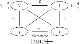
FIGURE 24.1 Relationship between fundamental circuit elements. (P. Junsangsri, F. Lombardi, Design of a hybrid memory cell using memristance and ambipolarity, IEEE Transactions on Nanotechnology, 12(1), 71–80. © (2013) IEEE. With permission.)
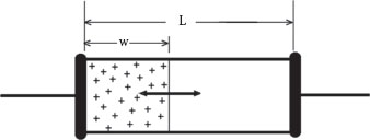
FIGURE 24.2 TiO2 film sandwiched between two Pt electrodes. (P. Junsangsri, F. Lombardi, Design of a hybrid memory cell using memristance and ambipolarity, IEEE Transactions on Nanotechnology, 12(1), 71–80. © (2013) IEEE. With permission.)
(24.2) |
where w(t) is the width of the doped region and L is the TiO2 thickness [4]. As a function of time, the width of the doped region is given by
(24.3) |
where μv represents the average dopant mobility (~10−10 cm2/s/V). By differentiating w(t) in (24.3) with respect to time, the rate of change for the width of the doped region is given by
(24.4) |
To model the characteristics of a memristor, different HSPICE models have been proposed in the technical literature [9, 10 and 11]. These HSPICE models are based on various window functions to simulate behaviorally and macroscopically a memristor according to its physical model. In this chapter, the memristor model of Ref. [9] is used because it has been shown to closely resemble the HP Labs memristor parameters and operation [5].
The memristor has received considerable attention over the last few years. For circuit design, the memristor has been widely advocated as a memory element, mostly for multilevel storage operation [12]. This is accomplished by using a reference (resistive) array, whose resistance values are predetermined and fixed. In this design, a comparator is used to compare the resistance of the memristor with a resistor in the array. As a memristor can attain a very high resistance, the required resistive array may cause a large power dissipation; moreover, the provision of a comparator in the cell may result in a considerable area overhead. In Ref. [13], the fundamental electrical properties of memristors are encapsulated into a set of compact closed-form expressions for characterizing nonvolatile memory operation. Moreover, the design, basic (READ and WRITE) operations, data integrity, and noise tolerance of these memory circuits are also established. In the design of Ref. [13], a memristor is read or written by directly forcing the input voltage source into the memristor itself and comparing it with the reference; so this memory requires three voltage levels (0, VDD, and VDD/2), and therefore an additional voltage line is needed. Area and power dissipation are considerably increased. In Ref. [6], a memristor-based content addressable memory (MCAM) is proposed; also, in this case, two levels of supply voltage (0, VDD and VDD/2) are required, thus incurring the same disadvantages in terms of area and power dissipation as in Ref. [13].
As opposed to a traditional (unipolar silicon CMOS) device whose behavior (either p-type or n-type) is determined at fabrication, ambipolar devices can be operated in a switched mode (from p-type tontype, or vice versa) by changing the gate bias [14,15]. Ambipolar conduction is characterized by the superposition of electron and hole currents; this behavior has been experimentally reported in different emerging technologies, such as carbon nanotubes [16], graphene [17], silicon nanowires [14,18], organic single crystals [19], and organic semiconductor heterostructures [20]. An ambipolar transistor can be used to control the direction of the current based on the voltage at the so-called polarity gate. In this chapter, a four-terminal ambipolar transistor (double gate MOSFET or DG-FET) is utilized. The second gate (referred to as the polarity gate, PG) controls its polarity, that is, when PG is “0,” the ambipolar transistor behaves like an N-channel metal oxide semiconductor (NMOS); when PG is “1,” it behaves like a P-channel metal oxide semiconductor (PMOS) [21]. The symbol and the modes of operation of the ambipolar transistor used in this chapter are shown in Figure 24.3.
In the technical literature and to the best knowledge of the authors, there is no HSPICEcompatible model to simulate the behavior of an ambipolar transistor; therefore, in this chapter, the model of Figure 24.4 is utilized at a macroscopic level for simulating the characteristics of an ambipolar transistor by using the transmission gates and MOSFETs. From this model, the characteristics of an ambipolar transistor that behaves like an NMOS or PMOS (based on the voltage at PG) are simulated. Figure 24.5 shows the relationship between the ambipolar current (ID) and the voltage across the drain and source of the ambipolar transistor (VDS) of Figure 24.4 as found by simulation at 32 nm feature size.
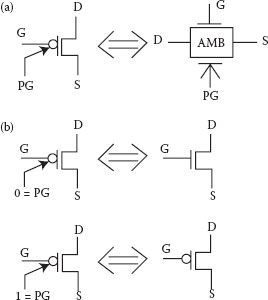
FIGURE 24.3 Ambipolar transistor. (a) Symbol. (b) Characteristic. (P. Junsangsri, F. Lombardi, Design of a hybrid memory cell using memristance and ambipolarity, IEEE Transactions on Nanotechnology, 12(1), 71–80. © (2013) IEEE. With permission.)
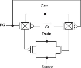
FIGURE 24.4 Model of an ambipolar transistor. (P. Junsangsri, F. Lombardi, Design of a hybrid memory cell using memristance and ambipolarity, IEEE Transactions on Nanotechnology, 12(1), 71–80. © (2013) IEEE. With permission.)
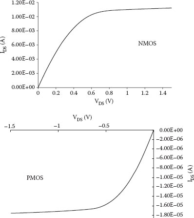
FIGURE 24.5 ID and VDS of an ambipolar transistor using the model of Figure 24.4 when biased as PMOS and NMOS.
By exploiting the characteristics of a memristor, a novel design of a memory cell is proposed in this section; as shown in Figure 24.6, a memristor is used as a storage element, while the ambipolar transistors are used as control elements. The new memory cell is obtained by connecting the memristor and two ambipolar transistors in series (Figure 24.6). In the proposed memory cell, data are sent through the bit line (BL) and the inverse bit line (BL′), while the word line (WL) is used for line selection. When the memory cell is selected, the voltage at WL is set to VDD and data are sent through BL and BL′. BL′ and L2 are connected by the transistor NT2; L2 is also connected to the PG of the ambipolar transistors. Therefore, in the proposed design, BL′ is used for polarity selection during the READ/WRITE operation. When BL′ is “0,” the ambipolar transistors behave as NMOS, and the current flows from node A to B (Figure 24.6), or from the drain side to the source side of the ambipolar transistors (node A is the source of AMB1 and node B is the drain of AMB2). If BL′ is “1,” the ambipolar transistors behave as PMOS. The current flows from node B to node A, or from the source to the drain of the ambipolar transistors. Hence, the memristor is written along both directions, that is, the WRITE operation is bidirectional. To understand the characteristics of the circuit in Figure 24.6, assume that WL is high (logic “1”) when selecting the memory cell. The memristance is equal to RON when the boundary of the TiO2 film in the memristor moves to the right side; this is accomplished by forward biasing the voltage across the memristor. For ROFF memristance, it is accomplished by reverse biasing the voltage across the memristor to move the boundary of the TiO2 film in the memristor to the left side. The READ and WRITE operations of the proposed memory cell are as follows.
In the proposed cell, the memristor is written with the data on BL and BL′. Owing to the symmetric conductance of the n and p types of the ambipolar transistors, the currents that flow in and out of the memristor are equal.
To WRITE a “1,” the memristance must be biased to RON, that is, BL and BL′ are set to VDD and ground (GND), respectively. The NMOS transistors (NT1 and NT2) can pass the GND value with no significant voltage drop across them, so the GND voltage from BL′ is passed to line L2. L2 is connected to the polarity gate of the ambipolar transistors; so when the voltage at L2 is GND, both ambipolar transistors behave as NMOS. For BL, owing to the voltage drop across the transistor NT1, the voltage at line L1 (VL1) is given by
(24.5) |
where VDD is the supply voltage and VNT1 is the threshold voltage of the transistor NT1.
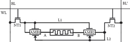
FIGURE 24.6 Proposed memory cell design. (P. Junsangsri, F. Lombardi, Design of a hybrid memory cell using memristance and ambipolarity, IEEE Transactions on Nanotechnology, 12(1), 71–80. © (2013) IEEE. With permission.)
Consider the ambipolar transistor AMB1; in Figure 24.6, the gate and drain of AMB1 are connected together by L1, and VGS and VDS of AMB1 are equal; therefore, AMB1 operates in the saturation region (VDS ≥ VGS − VT and VGS > VT). The voltage at node A of the memory cell in Figure 24.6 (VA) is
(24.6) |
where VDS1 is the voltage between the drain and the source of AMB1.
Next, consider the ambipolar transistor AMB2; assume the memristor holds as data a “0” (ROFF) prior to the WRITE “1” operation. The memristance ROFF is relatively high, so the voltage drop across the memristor (Vmem) is also high, thus resulting in a high voltage difference between nodes A and B, where VA is given in Equation 24.6 and VB is nearly GND. For AMB2, VGS2 is also relatively high (nearly VL1), while VDS2 is relatively low (nearly zero); so AMB2 operates in the linear region. Owing to the voltage drop across the memristor, the boundary of the memristor changes and its memristance is reduced during the WRITE “1” operation. When the memristance is reduced, Vmem is also reduced. The voltage at node B increases when reducing the voltage difference across the memristor. The voltage at node B increases until AMB2 operates in the saturation region (VDS2 ≥ VGS2 – VT2), where VDS2 is the voltage difference between node B and L2, VGS2 is the voltage difference between L1 and L2, and VT2 is the threshold voltage of AMB2. So the total current that passes through AMB1, AMB2, and the memristor suddenly increases; then VB (VA) increases (decreases) at a higher rate as shown in Figure 24.7. Figure 24.7 shows the plot of the voltage at nodes A and B, and the memristance of the memory cell versus time (ns). As explained previously, the voltage at node A (B) slightly decreases (increases) first; when the memristance reduces till VDS2 ≥ VGS2 – VT2, AMB2 operates in the saturation region, and the voltage at node A (B) suddenly decreases (increases).
The process for writing a “0” is similar to the one for writing a “1,” but with the inverted logic value. For writing a “0,” the memristor must be in the ROFF state. BL is at GND (i.e., 0), while BL′ is at VDD (i.e., 1). As BL′ is at VDD, the ambipolar transistors behave as PMOS and are ON (BL is “0”). Then the memristor is in the ROFF state because the voltage at node B is higher than at A (or the current flows from L2 to the drain of AMB2).
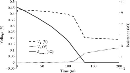
FIGURE 24.7 Plot of voltage, resistance (y-axis), and time (x-axis) for the proposed memory cell.
Consider next the READ operation. Recall that the memristor will change its memristance value if there is a current or voltage across it. To prevent this from happening, the READ operation must be fast; in particular, it should be faster than the time required for reaching the threshold time of the memristor (given by 12 ns [6]). In the proposed cell, the READ operation occurs by precharging the bit lines (BL and BL′) to VDD and GND, respectively, and WL is then set. Similar to the WRITE “1” operation, both AMB1 and AMB2 are ON during the first part of the READ operation. The voltages of the bit lines are precharged to their appropriate value; when connected through the ambipolar transistors and memristor, the voltages of the bit lines tend to balance their values, that is, the voltage of BL is transferred to BL′. When the voltage of BL′ is increased up to a value higher than the threshold voltage of the ambipolar transistors, the ambipolar transistors behave as PMOS, that is, L1 and L2 are disconnected. So the voltage difference between BL and BL′ is dependent on the data in the memory cell, that is, the memristance value. When the memristance of the memory cell is RON, the voltage across the memristor is very low. The voltage difference between BL and BL′ is lower than when the memristance is ROFF because the voltage from BL is better transferred to BL′ and the voltage difference between the bit lines for RON is less than for ROFF. Consider the voltage difference across the memristor during a READ operation; the ambipolar transistors are OFF, so the voltage difference across the memristor drops to zero. As both ambipolar transistors are OFF, the voltage difference between the bit lines does not affect the memristance of the memory cell.
HSPICE [22] has been used to simulate the characteristics of the proposed memory cell; the memristor model from Ref. [8] (with a memristance range of 100–19 kΩ) is employed. The macroscopic model of Figure 24.4 is utilized for an ambipolar transistor; the transistor sizes are then adjusted to generate the symmetric conduction between the PMOS and NMOS behaviors. In this chapter, the NMOS and PMOS transistors of the macroscopic model of Figure 24.4 have a feature size of 32 nm [23]. The circuit is then designed by setting Leff = 12.6 nm, Vth = 0.16 V (NMOS) or −0.16V (PMOS), VDD = 0.9 V, and Tox = 1 nm. The WRITE driver of Figure 24.8 [24] is utilized for the two memory operations (WRITE and READ).
In this section, the WRITE operation is simulated. Recall that the memristor retains its value when the timing of the voltage difference across the memristor is less than 12 ns [6]. To simulate the WRITE operation, the WRITE time of a memristor can be found by considering the memristance of the memory cell. The WRITE time is the time to fully bias the memristor to its desired state, so this is a function of the value of the memristance. Figure 24.9 shows the plot of the memristance range (x-axis) versus the WRITE time (y-axis) of the proposed memory cell when using the model of Ref. [9]. Figure 24.9 shows that by increasing the memristance range, the WRITE time is increased too; the WRITE time is 219 ns for the considered memristor (with a memristance range of 100–19 kΩ).
FIGURE 24.8 Driver circuit for WRITE operation. (P. Junsangsri, F. Lombardi, Design of a hybrid memory cell using memristance and ambipolarity, IEEE Transactions on Nanotechnology, 12(1), 71–80. © (2013) IEEE. With permission.)
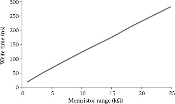
FIGURE 24.9 Plot of WRITE time (ns) versus memristance range (kΩ).
Using the driver circuit in Figure 24.8, when WE is ON, BL and BL′ are precharged to VDD and GND, respectively, prior to the READ operation. So the voltage at node IN in Figure 24.8 is VDD. Next, WE is OFF to isolate the input voltage from node IN and the bit lines (BL and BL′). So WL is ON to start the READ process. Simulation of the READ operation shows that the voltage differences between BL and BL′ for the “1” (RON) and “0” (ROFF) states are not the same; for a 1 ns READ operation, the voltage difference between BL and BL′ in the “1” state (RON) is about 0.1205 V, while it is 0.5817 V for the “0” state (ROFF). Moreover, the proposed memory cell is similar in behavior to an SRAM because the voltage is kept within L1 and L2 when there is no READ/WRITE operation. By opening only WL, the voltages from L1 and L2 are sent to BL1 and BL2, respectively; then the memristor is read without disturbing its current state.
Even though the memristance of the memory cell does not cause a state change, in some cases (such as if selecting the wrong threshold voltage for the ambipolar transistor when it is operating as a PMOS), the memristance may slightly change its value during a read “0” (ROFF) operation. Following the precharging of BL and BL′, every time the memory cell is read, it is biased to the RON state, that is, if it is already in the RON state, its value must be unchanged. The READ time is established by considering the rate of change in memristance from ROFF to RON. Hence, multiple WRITE operations with alternating values are simulated. As shown in Figure 24.10, two WRITE operations are used, that is, the memristor changes from ROFF to RON (write “1”), and from RON to ROFF (write “0”).
As shown in Figure 24.11, the shaded region corresponds to the WRITE time (TW) when the memristor is changed from ROFF to RON. By considering the slight memristance rate of change in value every time a READ operation occurs, a state change (i.e., from ROFF to RON) can occur after multiple and consecutive READ operations. Therefore, a refresh operation is required. Let the memristance value (given by ROFF/2) be the threshold level for the READ operation; when this value is reached, a refresh operation must take place to prevent the memristor from changing its state. So the READ time is given by
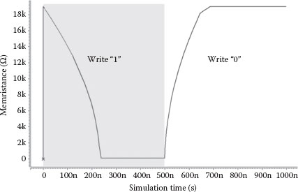
FIGURE 24.10 Memristance of the proposed memory cell (y-axis) versus time (x-axis) for consecutive WRITE “1” and “0” operations.
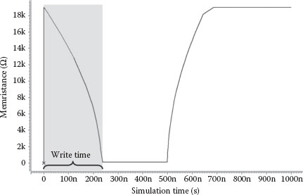
FIGURE 24.11 Memristance of the proposed memory cell (y-axis) versus time (x-axis) for consecutive WRITE “1” and “0” operations.
(24.7) |
where TR is the READ time, TW is the WRITE time, and N is the number of consecutive READ operations. By considering ROFF/2 as the threshold level of the memristance, half of the WRITE time (TW/2) corresponds to the time to reach the threshold level, that is, when the memristance of the proposed memory cell reaches this threshold level, a refresh operation is required.
As mentioned previously in the ROFF state, the READ operation slightly changes the memristance value up to a possible change of state, that is, from ROFF to RON. To avoid this state change from occurring, a refresh operation is required. For detecting the voltage difference between BL and BL′ (VDIFF), a comparison circuit is needed; if the memristor is in the ROFF state and VDIFF is lower than the voltage difference between the bit lines (when the memristance is equal to half of ROFF), the refresh operation must start by rewriting “0” to the memory cell. In the proposed memory cell, the READ operation is affected only for “0” (i.e., the ROFF state), because the voltage difference between the bit lines biases the memristor to RON.
Consider next the size of the transistors; there are some trade-offs between the transistor size (NT1, NT2, and the ambipolar transistors in Figure 24.6), the WRITE time, and the number of READ operations for assessing the impact of the change in memristance. For a large transistor size, the voltage from BL or BL′ will be transferred faster to the memristor, thus resulting in a low WRITE time. However, the number of READ operations is also small, because there is a high voltage across the memristor, that is, a high rate of change is applicable to the memristance.
Figure 24.12 shows the plots of the WRITE and READ times (ns) versus the transistor size (nm). This graph shows that if the transistor size increases, the WRITE time decreases because the NMOS transistors allow a higher bias from the bit lines (BL and BL′) to the memristor. As for the READ time, it is more than 200 times less than the WRITE time, but it shows the same dependency versus the transistor size. Moreover, for the READ time, by increasing the transistor size, the voltage across the memristor will increase, and the rate of change for the memristance will also be high. Therefore, by considering that the memory cell must be read nearly 100 times consecutively before changing its state, the utilization of small-sized transistors will result in a slower WRITE time. By having a fast READ time, the data in the memory cell can be read more times prior to the point at which the memristor changes its state.
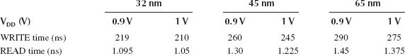
In this section, the proposed memory cell is analyzed with respect to its CMOS feature size; designs using 32, 45, and 65 nm [23] have been simulated. Two values for the supply voltage (i.e., 0.9 and 1.0 V) have been used. The results are given in Table 24.1. Table 24.1 shows that when the feature size is reduced, the WRITE and READ times decrease significantly too; moreover, the supply voltage significantly affects the WRITE and READ times. In Table 24.1, the READ time corresponds to the maximum value found over 100 consecutive READ operations (so without incurring in a change of state). By increasing the supply voltage, the WRITE time decreases; at a lower supply voltage, the voltage across the memristor is also lower and the change of memristance state occurs at a slower rate. So the WRITE time is also slower. The READ time reported in Table 24.1 corresponds to the maximum value for a READ operation as performed at least 100 times prior to reaching the threshold and changing the state of the memristance; hence, if the READ time is faster than the value given in Table 24.1, then the number of consecutive READ operations for state change (i.e., from ROFF to RON) is also larger.
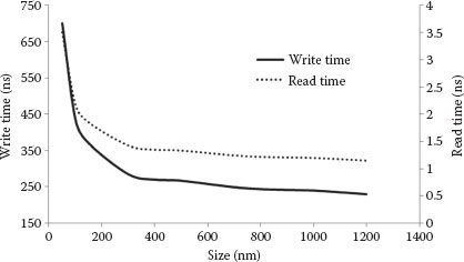
FIGURE 24.12 Plot of WRITE and READ times versus transistor size (NMOS).
TABLE 24.1
WRITE/READ Times at Different Supply Voltages and Feature Sizes
Next, consider the power dissipation of the proposed memory cell circuit; the memory cell consists of a small number of transistors (i.e., two NMOS transistors and two ambipolar transistors, so 4T). Based on the number of transistors, the capacitance of the proposed memory cell is less than a traditional RAM cell (requiring 6T). Also, the proposed circuit does not require standby power to retain the memristance value, and there is no direct path connecting VDD to GND. However, leakage power due to switching is still present, thus causing dynamic dissipation. This type of power dissipation is dependent on the clock frequency and is given by the well-known equation
(24.8) |
where PDyn denotes the dynamic power dissipation, V is the supply voltage (denoted by VDD), C is the capacitance, and fclk is the clock frequency. To reduce power dissipation, VDD as well as the clock frequency must be decreased. While technology scaling (such as 32 nm) operates at a low supply voltage, the reduction in frequency also implies degradation in performance. HSPICE has been used to simulate the power dissipation of the proposed memory cell using the macroscopic model presented previously. The simulation results show that the average power of the proposed memory cell is only 5.9% of the power in the MCAM cell of Ref. [6] also based on a memristor; the main reason for the reduction in power dissipation compared with Ref. [6] is that the supply voltage of the proposed memory cell (0.9 V) is significantly less than that of the MCAM cell (3 V).
In this section, a comparative discussion between the proposed memory cell and the MCAM of Ref. [6] is pursued. It should be noted that in Ref. [6], the MCAM has a different functionality as the search data operation is available to compare the stored data during the READ operation, that is, if the stored data is matched with the search data, the match line will be discharged, or else the original state will be preserved. As the proposed memory cell is binary, then for a READ operation, the stored value shows as a voltage difference between the two bit lines.
Ref. [6] requires two voltage sources, VDD and VDD/2 (and a VDD of 3 V). This is significantly higher than the supply voltage of the proposed cell (based on CMOS scaling). Simulation also shows that at the same supply voltage (i.e., 0.9 V), the proposed memory cell requires only 33.037% of the power of Ref. [6]. This is a direct result of the nonstatic power dissipation source in the proposed memory cell and the lower number of components in the circuit, that is, four transistors and one memristor, while Ref. [6] uses seven transistors and two memristors for a 7T NOR type, and five transistors and two memristors for the 5T NOR type.
As for the memory operations, simulation results show that the WRITE time of the proposed memory cell is slower than that of Ref. [6] because the voltage across the memristor of Ref. [6] (1.5 V) is higher than that of the proposed memory cell (0.9 V), that is, the rate of change of the memristor in the MCAM is faster than in the proposed memory cell. However, at the same supply voltage (0.9 V), the simulation results show that for WRITE, the proposed memory cell is slightly slower than the MCAM [6]. This occurs because in the proposed memory cell, the voltage drop across the transistors during a WRITE operation is high; so the voltage across the memristor in the proposed memory cell is less than half of the supply voltage. In the MCAM, the supply voltage (VDD/2) is directly forced to the memristor for a WRITE operation; so the WRITE time of the MCAM [6] is not affected by the voltage drop across the transistor. By reducing the voltage drop across the transistors, the WRITE time of the proposed memory cell can be improved with respect to the MCAM of Ref. [6]. As for the READ time, this operation is significantly faster in the proposed cell (1 ns) than in Ref. [6] (12 ns) because in Ref. [6] the search time is dependent on the discharging process of the match line.
This chapter presented a novel memory cell whose circuit consists of a memristor, two NMOS, and two ambipolar transistors, and hence its hybrid nature. In this cell, the memristor is utilized as a storage element due to the excellent features such as nonvolatility, linearity, low power consumption, and good scalability. The proposed hybrid cell also utilizes ambipolar transistors for the control of the memristance in the operation of the memory cell. The hybrid memory cell has been analyzed with respect to the two memory operations (READ and WRITE) and the characteristics of the memristor range for its on/off states.
Macroscopic models are utilized to characterize the nonvolatile feature of the memory cell. In the proposed memory cell, during the READ operation, the voltage across the memristor is low; so a refresh operation may be required when multiple consecutive READ operations occur. This operational feature is also related to the substantial difference in the READ and WRITE times (nearly two orders of magnitude) and the memristance range. Extensive simulation results using HSPICE have been provided to substantiate the performance of the proposed memory cell; different metrics (READ time, WRITE time, power dissipation) have also been assessed under different operating conditions (such as by varying the feature size and supply voltage).
1. G.I. Bourainoff, P.A. Gargini, D.E. Nikonov, Research directions beyond CMOS computing, Solid-State Electronics, 51(11–12), 1426–1431, 2007.
2. D. Akinwande, S. Yasuda, B. Paul, S. Fujita, G. Close, H.S.P. Wong, Monolithic integration of CMOS VLSI and CNT for hybrid nanotechnology applications, Proceedings of the 38th European Solid-State Device Research Conference, ESSDERC’08, pp. 91–94, 2008.
3. N. Engheta, Circuit with light at nanoscales: Optical nanocircuits inspired by metamaterials, Science, 317(5845), 1698–1702, 2007.
4. D.B. Strukov, G.S. Snider, D.R. Stewart, R.S. Williams, The missing memristor found, Nature, 453, 80–83, 2008.
5. L.O. Chua, Memristor—The missing circuit element, IEEE Transactions on Circuit Theory, CT-18(5), 507–519, 1971.
6. K. Eshraghian, K.R. Cho, O. Kavehei, S.K. Kang, D. Abbott, S.M. Steve Kang, Memristor MOS content addressable memory (MCAM): Hybrid architecture for future high performance search engines, IEEE Transactions on VLSI Systems, 19(8), 1407–1417, 2011.
7. P. Junsangsri, F. Lombardi, Design of a hybrid memory cell using memristance and ambipolarity, IEEE Transactions on Nanotechnology, 12(1), 71–80, 2013.
8. S. Williams, How we found the missing memristor, IEEE Spectrum, 45(12), 28–35, 2008.
9. D. Batas, H. Fiedler, A memristor SPICE implementation and a new approach for magnetic flux controlled memristor modeling, IEEE Transactions on Nanotechnology, 99, 1–1, 2009.
10. Z. Biolek, D. Biolek, V. Biolova, SPICE model of memristor with nonlinear dopant drift, Radioengineering, 18(2), pt. 2, 210–214, 2009.
11. A. Rak, G. Cserey, Macromodeling of the memristor in sPICE, IEEE Transactions on Computer-Aided Design of Integrated Circuits and Systems, 29(4), 632–636, 2010.
12. H. Kim, M. Pd. Sah, C. Yang, L.O. Chua, Memristor-based multilevel memory, 12th International Workshop on Cellular Nanoscale Networks and Their Applications (CNNA), 2010.
13. Y. Ho, G.M. Huang, P. Li, Nonvolatile memristor memory: Device characteristics and design implications, ICCAD’09, November 2–5, 2009, San Jose, California, USA.
14. S. Koo et al., Enhanced channel modulation in dual-gated silicon nanowire transistors, Nano Letters, 5(12), 2519–2523, 2005.
15. Y. -M. Lin et al., High-performance carbon nanotube field-effect transistor with tunable polarities, IEEE Transactions on Nanotechnology, 4, 481–489, 2005.
16. S. Heinze et al., Unexpected scaling of the performance of carbon nanotube Schottky-barrier transistors, Physical Review B, 68, 235418, 2003.
17. K.S. Novoselov et al., Electric field effect in atomically thin carbon films, Science, 306(5696), 666–669, 2004.
18. A. Colli et al., Top-gated silicon nanowire transistors in a single fabrication step, ACS Nano, 3(6), 1587–1593, 2009.
19. A. Dodabalapur et al., Organic heterostructure field-effect transistors, Science, 269(5230), 1560–1562, 1995.
20. J.H. Schön et al., Ambipolar pentacene field-effect transistors and inverters, Science, 287(5455), 1022–1023, 2000.
21. M.H. Ben Jamaa et al., Novel library of logic gates with ambipolar CNTFETs: Opportunities for multilevel logic synthesis, DATE2009, 2009, pp. 622–627.
22. Star-Hspice User Guide, Avant! Corporation, Release 2002. 2 June 2002.
24. CMOSSRAM Circuit Design and Parametric Test in Nano-Scaled Technologies Frontiers in Electronic Testing, 2008, Volume 40, 13–38.