
Low-Stress Transfer of Graphene and Its Tunable Resistance by Remote Plasma Treatments in Hydrogen |
CONTENTS
In this chapter, a novel, low-stress process for transferring thermal chemical vapor deposition (CVD) single-layer graphene from copper foils to destination substrates is demonstrated. An efficient transfer of graphene by directly fishing up the graphene with the target substrate rather than by using the “poly(methyl methacrylate) (PMMA)-based transfer” method is reported. Electrical and optical characteristics of the as-transferred graphene and the hydrogen remote-plasma-modified graphene are presented. Although graphene is mechanically very strong considering its atomically thin structure, a large-area, single-layer graphene is practically very fragile, especially during handling and transfer from one substrate to another. Handling of a large-area freestanding graphene is even more challenging. The combination of effective transfer and surface treatment of graphene by hydrogenation allows the fine-tuning of its electrical resistivity for practical applications.
Since the isolation and confirmation of a stable, atomically thin graphene of a 2D graphite-like carbon network, many means of synthesizing and a wide variety of applications of graphene and modified graphene have been proposed or demonstrated. Graphene film has been attracting much attention because of its exceptional properties, such as extremely high electron mobility [1], low resistivity [2], high thermal conductivity [3,4], and high mechanical strength [5]. Graphene is a promising material for advanced device applications in the future.
Graphene film can be synthesized on catalyst layers such as copper [6,7] and nickel foil [8] by using CVD. For future applications of graphene, the large-scale growth and transfer of graphene from the catalyst are required, and the graphene film must be exfoliated from the catalyst to be integrated to the appropriate surface for further applications. Graphene film might need to be placed on a substrate that is not compatible with the synthesis conditions for graphene. Therefore, an effective transfer process is needed to remove graphene from where it is grown and transfer it to where it will be used. The extremely thin, single-layer graphene of one atom thickness makes a damage-free transfer process even more challenging. Besides, the removal of substance between the transferred graphene and the destination substrate must start from the center toward the edges of the graphene. Otherwise, the trapping of undesired substance between the transferred graphene and the destination substrate will be an issue. For some applications, it is also desirable for more than one graphene film to be transferred to the same destination substrate to form a stacked structure of graphene films of the same or different characteristics.
A few transfer processes have been reported. Generally, coatings on graphene, such as PMMA, have been used as a mechanical support to transfer graphene after the underlying catalyst is etched away with acid solution (e.g., HCl, NHO3, and FeCl3) [9, 10 and 11] for several hours. PMMA is then etched away after the graphene is transferred and placed on top of the destination substrate. Stress is induced in the graphene during the transfer and curing process of PMMA. A second coating of PMMA was found to dissolve the first coating and help relax the stress on the graphene. The suggested multiple coatings of PMMA and the need to etch it for exposing the graphene add three more process steps and consume additional chemicals. For applications, that require the transfer of multiple graphene films of the same or different properties, the process is even more complicated and tedious because PMMA needs to be coated and etched repetitively. Furthermore, the graphene film showed strong n-type doping after using PMMA to support and transfer to substrate. Perhaps the residual of PMMA remaining on the graphene, which induced the charge transfer, evidently occurs at the interface between graphene and PMMA, the residual still left on the graphene surface even when the PMMA has been removed by acid solution [12]. However, a “direct transfer method” has been reported by the Ruoff group [7,13], and the graphene process method not only shows more easier transfers and shorttime consumption but also it reduces the chemical damage of graphene from the solvent.
As reported in previous research works [14, 15 and 16], when graphene is fully terminated by hydrogen, the electrically conductive graphene is converted into electrically insulating graphane, which has direct band gaps with Eg = 3.5 eV for the chair form and with Eg = 3.7 eV for the boat form. The calculated graphane C–C bond length of 1.52 Å is similar to the sp3 bond length of 1.53 Å in diamond and is much greater than the 1.42 Å characteristics of sp2 carbon in graphene [17]. So the atomic structure is also different from that of graphene. Graphene has a 2D flat plane structure, whereas graphane has an extended 2D covalently bonded structure [17]. Moreover, what if only one side of the graphene carbon atoms is terminated with hydrogen atoms? It is called graphone, which has been calculated to have an indirect band gap of 0.46 eV. And it is ferromagnetic while graphene and graphane are nonmagnetic [18]. Therefore, it is possible to tune the electronic and magnetic properties of graphene by hydrogenation. The possibility of band gap engineering with hybrid graphane–graphene nanostructures is desirable and promising [19]. To achieve this, a novel handling and transfer process for synthesized graphene is necessary.
Here, we report a transfer process that is easy and of low stress to graphene; the number of layers and quality of the as-grown graphene and hydrogen-terminated graphene were evaluated by Raman spectroscopy. We also show that the resistance of graphene can be tuned by exposure to remote hydrogen plasma for different periods of time. The Raman spectra of as-transferred and modified graphene are compared to show the structural modification of graphene by the hydrogen plasma.
Graphene was grown by thermal CVD on copper foils of 50 μm thickness in a gas mixture of methane and hydrogen at a temperature about 1000°C at 1 Torr gas pressure or lower. A transfer process with minimized stress to graphene without requiring the coating of PMMA on graphene has been developed. Because the graphene film is one carbon atom thick, the thickness of graphene is only ~0.34 nm; to protect and locate the graphene, we stuck a Teflon tape to the edge of the graphene before we carried out the chemical etching process. The schematic and flowchart for the transfer process are shown in Figure 27.1a and b. Instead of using PMMA coatings, the graphene on copper remains floating on the surface of the aqueous chemicals and deionized (DI) water until the copper is completely etched away and the graphene is placed on top of a destination substrate. During the entire process, graphene is not picked up by any stressful process, but instead remains floating on the surface of the liquids. The destination substrate is placed in the liquid to accept the graphene when the liquid is drained and the graphene is lowered toward the substrates. A variety of modified transferring processes allows the graphene to be transferred in different kinds of supporting substrates, including various kinds of grids. Graphene with both sides exposed can be modified before being placed on another substrate.
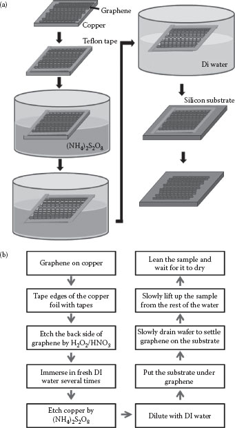
FIGURE 27.1 (a) Schematic diagrams, and (b) a flow chart representing a low-stress graphene transfer process.
Transferred graphene was subjected to remote microwave plasma generated in hydrogen at 1 Torr gas pressure as shown in Figure 27.2a. The distance between graphene and the plasma ball was about 10 cm with a metal screen between the plasma and the graphene. After exposing the remote plasma species for 10 min, the sample was taken out to measure its resistance. The electrical resistance of graphene was measured by depositing gold contacts on two sides of a nearly squareshaped graphene sheet. The geometry is shown in Figure 27.2. An ohmmeter was used to measure the resistance between these two gold contacts as shown in Figure 27.2b at a different time of the hydrogenation process. All experiments were executed at room temperature. Graphene and hydrogenated graphene were characterized by resistance measurements, optical microscopy, scanning electron microscopy (SEM), and Raman spectroscopy.
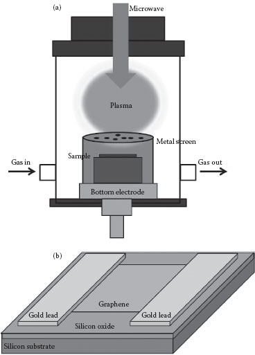
FIGURE 27.2 (a) Schematic diagram showing the remote hydrogenation plasma; and (b) Schematic diagram showing the geometry of graphene and electrodes for resistance measurements. (W. Chen et al., Low-stress transfer of graphene and its tuneable resistance by remote plasma treatments in hydrogen, 11th IEEE International Conference on Nanotechnology, Portland, Oregon, August 15–18. © (2011) IEEE. With permission.)
Figure 27.3a shows an optical photo of a single-layer graphene floating on DI water. There is a circle on the graphene. This graphene is successfully transferred from a copper foil to a silicon oxide/silicon substrate shown in Figure 27.3b. The graphene floating on liquids was in a relaxed state with minimum applied stress during the whole transferring process. Neither the protective coatings nor the mechanical handling tools were in touch with the graphene. This novel process makes it very useful for the graphene to be safely transferred from one substrate to another. It also allows further modification of the graphene in the middle of the transferring process. Therefore, stacking of multiple layers of graphene and modified graphene can be implemented effectively for a variety of innovative applications. Figure 27.3c is an SEM image showing the graphene after transfer.
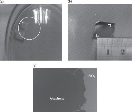
FIGURE 27.3 (a) Optical image showing graphene marked by a circle floating on DI water, (b) Optical photo of a transferred graphene on a destination substrate. (c) SEM image of a transferred graphene on an SiO2/Si substrate. The scale bar is 300 μm.
Figure 27.4 shows one example of the hydrogen-plasma-treated single-layer graphene. The optical micrograph shows the boundary between graphene and hydrogen-plasma-modified graphene. The different colors of graphene and hydrogen-plasma-modified graphene are due to the interference of these films of different atomic structure and thickness (graphene is about 0.34 nm thick, and when fully hydrogenated, graphane is about 2.62 nm thick). Part of the graphene was covered by an aluminum foil when the sample was treated by remote hydrogen plasma.
The resistance shown in Figure 27.5a was measured immediately after every hydrogen plasma treatment was completed for a fixed time period. At first, the resistance increased slowly from 0.90 kΩ. It increased to 200 kΩ abruptly at the last treatment. It can be speculated that when one hydrogen atom attacks one carbon atom to break the π bond, one unpaired electron will be released simultaneously. Owing to the π-bonding network breaking and the p-electron associated with the unhydrogenated carbon atoms being localized and unpaired, the energy of hydrogen bonding to the rest of the carbon atoms is lowered. As the amount of the broken π-bonding network increased, the trend is accelerated, and the resistance increases abruptly until carbon sites available for bonding to hydrogen reach saturation.
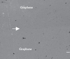
FIGURE 27.4 Optical micrograph showing the boundary between as-grown graphene and hydrogenated graphene as pointed by an arrow. The scale bar is 100 μm. (W. Chen et al., Low-stress transfer of graphene and its tuneable resistance by remote plasma treatments in hydrogen, 11th IEEE International Conference on Nanotechnology, Portland, Oregon, August 15–18. © (2011) IEEE. With permission.)
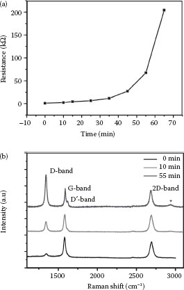
FIGURE 27.5 (a) Electrical resistance of a single-layer graphene as a function of exposure time to a remote hydrogen plasma. (b) The evolution of Raman spectra (633 nm laser excitation) with increasing exposure time to a remote microwave plasma in hydrogen. (0 min bottom; 55 min top.) (W. Chen et al., Low-stress transfer of graphene and its tuneable resistance by remote plasma treatments in hydrogen, 11th IEEE International Conference on Nanotechnology, Portland, Oregon, August 15–18. © (2011) IEEE. With permission.)
To investigate the transformation of graphene to graphane, the evolution of Raman spectra at different stages of hydrogen plasma treatment was monitored. These spectra are characterized by the presence of three typical bands in graphene and graphane. They are the disorder-induced D band at around 1344 cm−1, the radial breathing mode G band at around 1580 cm−1, and the second order of zone boundary phonons 2D band at around 2680 cm−1. As the plasma treatment time increased, the intensities of the two bands rose. A shoulder peak of the G band, called the D′ band, originating from an intervalley double resonance Raman process, where the associated phonons have small wave vectors in the vicinity of Γ point, can be observed. Another featured band assigned to the combination of the D band and the G band can be found at around 2924 cm−1, as pointed out by a star mark in Figure 27.5b. The appearance of the D′ band and the D + G peak indicates that graphene is turning into graphane by hydrogen termination. An increase in the ID/IG ratio was also examined.
These are all related to an increase in the amount of sp3 bonding. Thus, from the above data, we can know that the increase in resistance is a result of the hydrogenation of graphene.
A novel process for transferring thermal CVD-grown graphene on copper foils to destination substrates for practical applications is reported. The transferred graphene is subjected to reactions with remote microwave plasma in hydrogen. The electrical resistance of modified graphene as a function of plasma treatment parameters is reported.
We gratefully acknowledge the financial support by the Ministry of Education and the National Science Council in Taiwan via grants 99-2120-M-006-004 and 99-2911-I-006-504.
1. X. Du, I. Skachko, A. Barker, and E. Y. Andrei, Approaching ballistic transport in suspended graphene, Nature Nanotechnology 3, 491–495, 2008.
2. J. H. Chen, C. Jang, S. Xiao, M. Ishigami, and M. S. Fuhrer, Intrinsic and extrinsic performance limits of graphene devices on SiO2, Nature Nanotechnology 3, 206–209, 2008.
3. W. W. Cai, A. L. Moore, Y. Zhu, X. Li, S. Chen, L. Shi, and R. S. Ruoff, Thermal transport in suspended and supported monolayer graphene grown by chemical vapor deposition, Nano Letters 10, 1645–1651, 2010.
4. S. Chen, L. Brown, M. Levendorf, W. Cai, S.-Y. Ju, J. Edgeworth, X. Li et al., Oxidation resistance of graphene-coated Cu and Cu/Ni alloy, ACS Nano 5, 1321–1327, 2011.
5. F. Schedin, A. K. Geim, S. V. Morozov, E. W. Hill, P. Blake, M. I. Katsnelson, and K. S. Novoselov, Detection of individual gas molecules adsorbed on graphene, Nature Materials 6, 652–655, 2007.
6. X. Li, W. Cai, I. H. Jung, J. H. An, D. Yang, A. Velamakanni, R. Piner, L. Colombo, and R. S. Ruoff, Synthesis, characterization and properties of large-area graphene films, ECS Transactions 19, 41–52, 2009.
7. X. Li, W. Cai, L. Colombo, and R. S. Ruoff, Evolution of graphene growth on Ni and Cu by carbon isotope labelling, Nano Letters 9, 4268, 2009.
8. K. S. Kim, Y. Zhao, H. Jang, S. Y. Lee, J. M. Kim, K. S. Kim, J.-H. Ahn, P. Kim, J.-Y. Choi, and B. H. Hong, Large-scale pattern growth of graphene films for stretchable transparent electrodes, Nature Nanotechnology 457, 706–710, 2009.
9. X. Li, Y. Zhu, W. Cai, M. Borysiak, B. Han, D. Chen, R. D. Piner, L. Colombo, and R. S. Ruoff, Transfer of large-area graphene films for high-performance transparent conductive electrodes, Nano Letters 9, 4359–4363, 2009.
10. W. Regan, N. Alem, B. Aleman, B. Geng, C. Girit, L. Maserati, F. Wang, M. Crommie, and A. Zettl, A direct transfer of layer-area graphene, Applied Physics Letters 96, 113102, 2010.
11. X. Li, Y. Zhu, W. Cai, M. Borysiak, B. Han, D. Chen, R. D. Piner, L. Colombo, and R. S. Ruoff, Transfer of large-area graphene films for high-performance transparent conductive electrodes, Nano Letters 9(12), 4359–4363, 2009.
12. Geringer, D. Subramaniam, A. K. Michel, B. Szafranek, D. Schall, A. Georgi, T. Mashoff, D. Neumaier, M. Liebmann, and M. Morgenstern, Electrical transport and low-temperature scanning tunneling microscopy of microsoldered graphene, Applied Physics Letters 96, 082114, 2010.
13. X. Li, W. Cai, J. An, S. Kim, J. Nah, D. Yang, R. Piner et al., Large-area synthesis of high-quality and uniform graphene films on copper foils, Science 324, 1312, 2009.
14. D. C. Elias, R. R. Nair, T. M. G. Mohiuddin, S. V. Morozov, P. Blake, M. P. Halsall, A. C. Ferrari et al., Control of graphene’s properties by reversible hydrogenation: Evidence for graphane, Science 323, 610, 2008.
15. A. Gupta, G. Chen, P. Joshi, S. Tadigadapa, and P. C. Eklund, Raman scattering from high-frequency phonons in supported n-graphene layer films, Nano Letters 6(12), 2667–2673, 2006.
16. M. E. Kompan and D. S. Krylov, Detecting graphene–graphane reconstruction in hydrogenated nanoporous carbon by Raman spectroscopy, Technical Physics Letters 36, 1140–1142, 2010.
17. J. O. Sofo, A. S. Chaudhari, and G. D. Barber, Graphane: A two-dimensional hydrocarbon, Physical Review B 75, 153401, 2007.
18. J. Zhou, Q. Wang, Q. Sun, X. S. Chen, Y. Kawazoe, and P. Jena, Ferromagnetism in semihydrogenated graphene sheet, Nano Letters 9, 3867–3870, 2009.
19. Y. H. Lu and Y. P. Feng, Band-gap engineering with hybrid graphane–graphene nanoribbons, The Journal of Physical Chemistry C113, 20841–20844, 2009.
20. W. Chen, C.-H. Tu, K.-C. Liang, C.-Y. Liu, C.-P. Liu, and Y. Tzeng, Low-stress transfer of graphene and its tuneable resistance by remote plasma treatments in hydrogen, 11th IEEE International Conference on Nanotechnology, Portland, Oregon, August 15–18, 2011.