
High-Yield Dielectrophoretic Deposition and Ion Sensitivity of Graphene |
CONTENTS
28.2 Device Design and Fabrication
28.3 Dielectrophoresis Deposition of Graphene
28.4 Electrical Characteristics of Graphene
28.5 Ion Sensitivity of Graphene
Graphene research has attracted enormous attention since the discovery of the material in 2004 [1]. Graphene can be viewed as a two-dimensional (2D) honeycomb lattice that is constructed with a single layer of carbon atoms. It not only provides a unique structure for fundamental research but is also an ideal material for future nanoelectronics and sensor applications [2,3]. Graphene has demonstrated fascinating chemical, mechanical, and electrical properties. For example, when exposed to different gases, graphene can be chemically doped to either p-type or n-type [4]. A nanoindentation measurement of a freestanding monolayer graphene membrane using atomic force microscopy (AFM) shows that the material has an ultrahigh Young’s modulus of 1.0 TPa, which makes graphene one of the strongest materials ever measured [5]. Depending on the number of layers in the sheet, the electrical properties of graphene alter accordingly, changing it from a semiconductor to a metal, or vice versa [6].
However, owing to the single-atom thickness, the handling of graphene has become a major bottleneck in this field, especially in the development of practical devices. The most common method to generate graphene is mechanical exfoliation of bulk graphite [1,7]. Single- or double-atomic-layer graphene can be obtained after repeatedly peeling layers off the highly oriented pyrolytic graphite using scotch tapes. However, the process is time-consuming, unscalable, and has low yield and low repeatability. Consequently, this technique has been used primarily to create individual devices for the study of novel physics of graphene; it is not suitable for large-scale device fabrication. Alternatively, graphene can be directly grown on substrates with chemical vapor deposition (CVD) and epitaxy methods [8,9]. However, these methods have a limited choice of substrates, which are not entirely compatible with traditional semiconductors and insulators in electronic device fabrication. Recently, chemical methods have been developed to produce stable, homogeneous graphene solutions in large quantities [10]. Depositing graphene from the solutions provides an effective approach to integrate graphene into device fabrication.
Owing to the small dimensions of graphene, the fabrication of graphene-based devices usually relies on expensive and time-consuming electron-beam lithography systems. The seriesstyle fabrication and time-consuming processes used in the electron-beam lithography are not suitable for mass production of such devices. The CVD- and epitaxy-grown graphene can be processed using the traditional lithography-based techniques. However, further modifications are needed to enhance the compatibility of the related materials to the standard substrates used in the semiconductor industry. By contrast, dielectrophoresis, a simple electrical approach using alternating current (AC) signals can not only deposit nanoscale materials inexpensively, but also it can achieve large-scale assembly of materials over large areas [11]. This method has been successfully used in the controlled assembly of nanowires, carbon nanotubes, and graphene [11, 12 and 13]. Furthermore, it is a solution-based method that can fully utilize the latest advances in the production of graphene solutions.
Here, we demonstrate the controlled assembly of graphene sheets on a substrate with high precision and high yield. Prefabricated electrodes are used to generate strong electric fields in the solution. The dispersed graphene sheets are attracted by the fields and land on the substrate to bridge the electrodes. A thermal annealing step is carried out to enhance the adhesion between the graphene and the substrate. Electrical characterization of the deposited graphene is conducted by using it as a semiconducting material in a liquid-gated field-effect transistor (FET). The assembled graphene sheets demonstrate high sensitivity toward pH values in an aqueous environment with excellent reversibility and repeatability. The ion sensing mechanism of the graphene-based device is described and discussed in the chapter. Our study demonstrates that the dielectrophoresis process is an effective approach to fabricate graphene-based electronics and sensors for practical applications.
28.2 DEVICE DESIGN AND FABRICATION
The electrodes used for graphene assembly are fabricated on a 4-inch silicon wafer with a 200-nm-thick surface thermal oxide layer. They are fabricated with traditional optical lithography and metal wet etching to maintain low costs and scalability. The detailed fabrication process can be found in our previous reports [14, 15, 16 and 17]. Figure 28.1a illustrates an electrode design that contains arrays of tips on both sides. Each electrode contains 21 comb fingers on the edge. The designed width and length of each finger are w = 3 μm and l = 10 μm, respectively. The gap between the two opposite fingers is g = 3 μm. The comb-shaped electrodes enable strong and directional electric fields between the tips. Figure 28.1b shows a scanning electron microscopy (SEM) image of a pair of fabricated electrodes. The scale bar shown in the image is 100 μm.
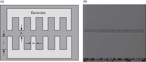
FIGURE 28.1 (a) Schematic illustration of an electrode design. (b) SEM image of a pair of fabricated electrodes.
The graphene solution is obtained from NanoIntegris (Skokie, IL, USA) with the single- to triple-atomic-layer graphene making up approximately 56% of the content. The sample has a concentration of 0.05 mg/mL and it is utilized as is without further chemical or physical modifications. During the dielectrophoresis process, a small drop of the graphene solution is placed on the substrate to cover the electrodes. The process takes 30–60 s with an instant voltage drop of 1–2 V observed from the oscilloscope during the graphene-capturing event. The dielectrophoretic assembly of graphene is based on the spatial redistribution of charges inside the material. The polarized graphene is subject to a net force and can be moved to follow the electric field direction. After removing the dispersion with a pipette, the deposited graphene is bonded to the substrate based on van der Waals forces. The use of electrodes in the graphene deposition process produces ready-to-use devices, and no further processing steps for electrical contacts are needed.
28.3 DIELECTROPHORESIS DEPOSITION OF GRAPHENE
The schematic diagram of the dielectrophoresis process is shown in Figure 28.2. A function generator is used as the AC source and an oscilloscope is used to monitor the voltage change during the graphene deposition process. The frequency and the peak-to-peak voltage of the AC signal are set as 5 MHz and 10 V, respectively. These parameters are selected based on our previous experimental studies on carbon nanotubes and analytical results from other groups [14, 15 and 16]. Because the capturing event of graphene on the device can cause a slight voltage drop across the electrodes, the voltage change displayed on the oscilloscope indicates the landing moment of the material.
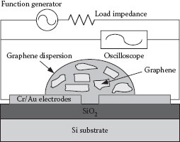
FIGURE 28.2 The experimental system for the dielectrophoretic deposition of graphene. (P. Li et al., High-yield dielectrophoretic deposition and ion sensitivity of graphene, in 2011 11th IEEE International Conference on Nanotechnology, Portland, OR, pp. 1327–1330. © (2011) IEEE. With permission.)
The dielectrophoretically assembled graphene sheets are inspected with SEM. Figure 28.3 shows the assembled graphene sheets on the electrodes. Multiple sheets are deposited between the electrodes to form conductive channels. Such graphene sheets can only be observed in between the electrode tips where the electric field has the highest magnitude during the dielectrophoresis process. This proves that dielectrophoresis is an “active” approach to assemble graphene and is suitable for device integration. On this particular device, we find that 13 out of 21 pairs of fingers are connected by graphene (marked as ellipses) with no graphene observed on the remaining 8 pairs (marked as X). This is because the graphene deposited in the early stage decreases the potential across the electrodes, changing the electric field distribution in the solution. Consequently, the dielectrophoretic forces on the dispersed graphene are weakened to a level where they are not able to drag the graphene sheets to the electrodes for further deposition. Nevertheless, the number of deposited graphene sheets is adequate for the graphene-based device to be functional. We believe that the yield of the graphene deposition on the electrode fingers can be improved by further optimization of the electrode design.
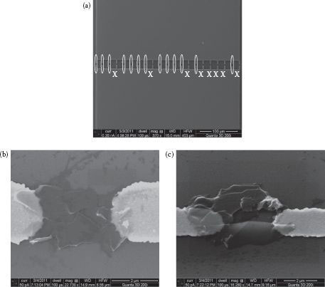
FIGURE 28.3 SEM images of the dielectrophoretically deposited graphene sheets. (a) Top view of a device with 21 electrode fingers. (b) Top view and (c) tilted view of the deposited graphene. (P. Li et al., High-yield dielectrophoretic deposition and ion sensitivity of graphene, in 2011 11th IEEE International Conference on Nanotechnology, Portland, OR, pp. 1327–1330. © (2011) IEEE. With permission.)
The deposited graphene sheets are then treated with a thermal annealing step at 200°C for 10 min on a hot plate. This step serves two purposes. First, it can reduce the contact resistance between the graphene and the electrode, resulting in an improved contact [11]. The electrical characteristics of the graphene sheets before and after the annealing step are illustrated in Figure 28.4. The resistance of this particular device decreases by 41%, from 345.13 to 202.17 Ω. Although not all the devices demonstrate the same trend of decreased resistance, previous investigations by other groups have proven that the effective electrical contact can be improved [18,19]. Second, we discover that the thermal annealing step can dramatically increase the adhesion between the graphene and the substrate. In our pH sensing experiments that involve intensive solution placing and removing steps, the thermally annealed devices demonstrate much higher repeatability than the nonannealed counterparts. Based on the fact that the nonannealed devices often show sudden, irreversible increase in resistance, we believe that the loosely bonded graphene sheets can be washed away in the solution removing steps. Although similar phenomena have occasionally been observed in thermally annealed devices, they are rare and the corresponding resistance decrease shows much smaller values. Therefore, we believe that the discrepancy between the two groups of devices originates from the bonding strength of the graphene and the substrate.
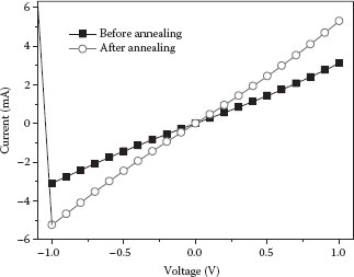
FIGURE 28.4 Current–voltage (I–V) characteristics of deposited graphene before and after thermal annealing at 200°C for 10 min. (P. Li et al., High-yield dielectrophoretic deposition and ion sensitivity of graphene, in 2011 11th IEEE International Conference on Nanotechnology, Portland, OR, pp. 1327–1330. © (2011) IEEE. With permission.)
28.4 ELECTRICAL CHARACTERISTICS OF GRAPHENE
The deposited graphene is electrically characterized using a liquid-gated FET configuration. The measurement system setup for the graphene-based transistor is shown in Figure 28.5. The two electrodes, previously used for the nanomaterial deposition, now serve as source and drain terminals. A droplet of distilled water is place on the substrate to cover the graphene. It is used as the liquid gating medium, as suggested by previous research reports [20,21]. A standard Ag/AgCl reference probe, serving as the gate electrode, is immersed in the water droplet. The suspended end is approximately 2 mm away from the graphene. A semiconductor device analyzer is used to apply the drain (Vd) and gate (Vg) voltage, and record the induced drain current (Id) at the same time.
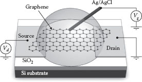
FIGURE 28.5 Schematic of a graphene-based field-effect transistor with an Ag/AgCl reference probe as the gate electrode.
The output characteristics (Id–Vd) of the graphene-based device are shown in Figure 28.6a. The drain voltage Vd is swept from −1 to 1 V with a 0.01 V step and the gate voltage is swept from −0.4 to 0.4 V with a 0.2 V step. The relationship between the drain current and drain voltage is highly linear in the measured range of −1 V to 1 V. This range is selected to protect the device from burning out by high current. Although drain current saturation is not observed, the field effect is apparent from the figure. Furthermore, we notice that when the gate voltage is shifted from a positive region to a negative region, the drain current becomes higher. This phenomenon indicates that graphene is a p-type material and a majority of its carriers are positively charged holes. During operation, the negative voltage can accumulate more holes into the channel area, leading to the higher drain current.
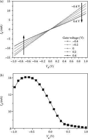
FIGURE 28.6 (a) Output characteristics of a graphene device with the reference gate voltage ranging from −0.4 to 0.4 V in 0.2 V steps. (b) Transfer characteristics of the same device with the gate voltage ranging from −1 to 1 V in 0.1 V steps. The drain current is fixed at −1 V.
The transfer characteristics (Id–Vg) of the same device are shown in Figure 28.6b. The drain voltage is fixed at −1 V and the gate voltage is swept from −1 to 1 V with a 0.1 V step. The smallest current obtained in this curve is 8.08 mA at Vg = 1 V and the highest current of 14.07 mA is observed at a gate voltage of −0.7 V. On the right side of the highest point (or Vg from −0.7 to 1.0 V), the current decreases as the gate voltage increases. This means that fewer holes are involved in the current conductance at a higher voltage, proving the p-type characteristics of the deposited graphene. On the other side of this point, as Vg decreases from −0.7 to −1 V, the current is decreased. This can be explained by the depletion of the minority carriers, electrons, from the graphene channel by the decreased negative gate voltage. In addition, when Vg is in the high, positive range of 0.5–1 V, the current plot is relatively flat with a saturation current of 8.1–8.3 mA. This indicates that graphene is a highly conductive material, which cannot be completely switched off using the current device configuration.
28.5 ION SENSITIVITY OF GRAPHENE
To investigate its potential in sensing applications, the deposited graphene is characterized for its response toward pH values in solutions. The electrodes initially used for dielectrophoresis are now used as electrical contacts. Figure 28.7 shows the system layout for the ion sensitivity measurement. The electrodes initially used for dielectrophoresis are now used as electrical contacts. A bias voltage V0 is applied across the electrode pair and the current I0 is monitored with a data acquisition system. Solutions with various pH values, ranging from 5 to 9 (standard buffer solutions from Fisher Scientific, Pittsburgh, PA, USA), are sequentially dropped on the device to cover the graphene. The assembled graphene is used as a two-terminal pH-sensitive resistor and its real-time resistance R in different solutions can be measured.
The graphene device shows a stable response toward pH values in liquid. Figure 28.8a shows the recorded data in a resistance–time (R–t) plot from the real-time data acquisition. The resistance of graphene is highly sensitive to pH values with the highest resistance (~475 Ω) at pH 5 and the lowest resistance (~405 Ω) at pH 9. A near-equal amount of decrement in the resistance of graphene can be observed when the pH value is changed from 5 to 9, and a similar amount of increment can be observed with increasing pH values. In addition, the graphene-based pH sensors show high repeatability among devices. The measurement of three different devices demonstrates that all sensors show similar electrical and ion-sensitive characteristics, as illustrated in Figure 28.8b. The normalized resistance, defined as
(28.1) |
is used to evaluate the sensor performance, where ΔR, Rr, Rmax, and Rmin are the real-time sensor resistances relative to its lowest value, the range of resistance in the entire measurement, the highest resistance, and the lowest resistance, respectively. Our measurement shows that the normalized resistance and the pH value have a relatively linear relationship, which can be expressed as
(28.2) |
As a result, the assembled graphene demonstrates reversible and repeatable pH sensitivity, enabling its potential in chemical- and bio-sensing applications.
The pH sensing mechanism of graphene can be explained by the electrolyte-induced capacitive gating principles that involve the adsorption of ions and the creation of an electrical double layer at the liquid–solid interface [22,23]. The hydroxonium ions (H3O+) and hydroxyl ions (OH−) from the pH buffer solution can be adsorbed on the graphene surface and create an electric double layer at the liquid–graphene interface. It is a nonfaradaic (or capacitive) process, which means the ions cannot transmit through the electric double layer directly. Instead, the energy transfer is achieved through the charging and discharging of this layer. The surface-adsorbed ions can attract mobile carriers with opposite charges from the graphene to the liquid–graphene interface, changing the conductance of the material. In our experiments, the surface-adsorbed ions in acidic solutions are primarily H3O+ ions, which can partially deplete the holes—the majority carriers—from the graphene. As a result, the resistance has a relatively high value in the pH 5 solution. In alkaline solutions, the surface-adsorbed ions are primarily OH− ions, which can accumulate extra holes in the graphene. Therefore, the resistance is decreased accordingly.
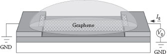
FIGURE 28.7 Testing scheme of deposited graphene in an aqueous environment. (P. Li et al., High-yield dielectrophoretic deposition and ion sensitivity of graphene, in 2011 11th IEEE International Conference on Nanotechnology, Portland, OR, pp. 1327–1330. © (2011) IEEE. With permission.)
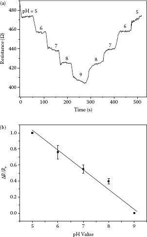
FIGURE 28.8 (a) Recorded real-time pH response of the assembled graphene. (b) Relationship between the normalized resistance and pH values. (P. Li et al., High-yield dielectrophoretic deposition and ion sensitivity of graphene, in 2011 11th IEEE International Conference on Nanotechnology, Portland, OR, pp. 1327–1330. © (2011) IEEE. With permission.)
Our research investigates the inherent pH sensitivity of graphene because the tested devices are configured as two-terminal resistors. The devices can also be configured as FET sensors with an additional terminal added to the device as a gate electrode. With the ability to control the amount of charge carriers in graphene through accumulation or depletion, the sensors may show enhanced performance. Two recent reports investigated the pH sensitivity of graphene using a liquid-gated transistor configuration [24,25]. Although their research was based on CVD- and epitaxy-grown graphene samples, the measurement technology can be easily extended to dielectrophoretically assembled graphene. Their results demonstrated enhanced pH sensitivity with nonzero gate voltages. One interesting effect presented in both reports is that the resistance–pH (R–pH) relationship switches its trend at a gate voltage of approximately −0.1 V. We expect that a similar phenomenon can be observed in the devices using dielectrophoretically assembled graphene. Additional experiments will be conducted to investigate the performance of the graphene transistor-based pH sensors.
In conclusion, we report a high-yield method to actively deposit graphene on prefabricated electrodes using dielectrophoresis. The electrode design enables highly concentrated electric fields to apply strong dielectrophoretic forces on graphene sheets in dispersion. The graphene sheets were precisely deposited on a substrate at the desired locations. Thermal annealing was used to improve the contact between the graphene and the electrodes as well as to enhance the adhesion between the graphene and the substrate. The use of electrodes in the deposition process enables the direct development of ready-to-use graphene devices, and no further processing steps for electrical contacts are needed. The deposited graphene demonstrated p-type characteristics when measured in a liquid-gated FET. The deposited graphene devices were used as sensors and they demonstrated satisfactory performance toward pH sensing. The electrical double layer at the liquid–graphene interface created by the capacitive gating effect was considered as the primary sensing mechanism. Our investigation shows that dielectrophoresis is a low-cost, simple, and fast method to deposit graphene and has great potential for device integration. We believe that the graphene-based sensors fabricated with this approach can be developed and applied to a wide range of areas in the near future.
1. K. S. Novoselov, A. K. Geim, S. V. Morozov, D. Jiang, Y. Zhang, S. V. Dubonos, G. IV, and A. A. Firsov, Electric field effect in atomically thin carbon films, Science, 306, 666–669, 2004.
2. P. Avouris, Graphene: Electronic and photonic properties and devices, Nano Lett., 10, 4285–4294, 2010.
3. A. K. Geim and K. S. Novoselov, The rise of graphene, Nat. Mater., 6, 183–191, 2007.
4. X. Wang, X. Li, L. Zhang, Y. Yoon, P. K. Weber, H. Wang, J. Guo, and H. Dai, N-doping of graphene through electrothermal reactions with ammonia, Science, 324, 768–771, 2009.
5. C. Lee, X. Wei, J. W. Kysar, and J. Hone, Measurement of the elastic properties and intrinsic strength of monolayer graphene, Science, 321, 385–388, 2008.
6. A. H. Castro Neto, F. Guinea, N. M. R. Peres, K. S. Novoselov, and A. K. Geim, The electronic properties of graphene, Rev. Mod. Phys., 81, 109–162, 2009.
7. N. Lei, P. Li, W. Xue, and J. Xu, Simple graphene chemiresistors as pH sensors: Fabrication and characterization, Meas. Sci. Technol., 22, 107002, 2011.
8. X. Li, W. Cai, J. An, S. Kim, J. Nah, D. Yang, R. Piner et al., Large-area synthesis of high-quality and uniform graphene films on copper foils, Science, 324, 1312–1314, 2009.
9. P. W. Sutter, J.-I. Flege, and E. A. Sutter, Epitaxial graphene on ruthenium, Nat. Mater., 7, 406–411, 2008.
10. S. Park and R. S. Ruoff, Chemical methods for the production of graphenes, Nat. Nanotechnol., 4, 217–224, 2009.
11. A. Vijayaraghavan, S. Blatt, D. Weissenberger, M. Oron-Carl, F. Hennrich, D. Gerthsen, H. Hahn, and R. Krupke, Ultra-large-scale directed assembly of single-walled carbon nanotube devices, Nano Lett., 7, 1556–1560, 2007.
12. A. Vijayaraghavan, C. Sciascia, S. Dehm, A. Lombardo, A. Bonetti, A. C. Ferrari, and R. Krupke, Dielectrophoretic assembly of high-density arrays of individual graphene devices for rapid screening, ACS Nano, 3, 1729–1734, 2009.
13. B. R. Burg, J. Schneider, S. Maurer, N. C. Schirmer, and D. Poulikakos, Dielectrophoretic integration of single- and few-layer graphenes, J. Appl. Phys., 107, 034302, 2010.
14. P. Li and W. Xue Selective deposition and alignment of single-walled carbon nanotubes assisted by dielectrophoresis: From thin films to individual nanotubes, Nanoscale Res. Lett., 5, 1072–1078, 2010.
15. P. Li, C. M. Martin, K. K. Yeung, and W. Xue, Dielectrophoresis aligned single-walled carbon nanotubes as pH sensors, Biosensors, 1, 23–35, 2011.
16. P. Li, N. Lei, J. Xu, and W. Xue, High-yield fabrication of graphene chemiresistors with dielectrophoresis, IEEE Trans. Nanotechnol., 11, 751–759, 2012.
17. P. Li, N. Lei, J. Xu, and W. Xue, High-yield dielectrophoretic deposition and ion sensitivity of graphene, in 2011 11th IEEE International Conference on Nanotechnology, Portland, OR, 2011, pp. 1327–1330.
18. D. Joung, A. Chunder, L. Zhai, and S. I. Khondaker, High yield fabrication of chemically reduced graphene oxide field effect transistors by dielectrophoresis, Nanotechnology, 21, 165202, 2010.
19. B. R. Burg, F. Lutolf, J. Schneider, N. C. Schirmer, T. Schwamb, and D. Poulikakos, High-yield dielectrophoretic assembly of two-dimensional graphene nanostructures, Appl. Phys. Lett., 94, 053110, 2009.
20. S. Rosenblatt, Y. Yaish, J. Park, J. Gore, V. Sazonova, and P. L. McEuen, High performance electrolyte gated carbon nanotube transistors, Nano Lett., 2, 869–872, 2002.
21. D. W. Kim, G. S. Choe, S. M. Seo, J. H. Cheon, H. Kim, J. W. Ko, I. Y. Chung, and Y. J. Park, Selfgating effects in carbon nanotube network based liquid gate field effect transistors, Appl. Phys. Lett., 93, 243115, 2008.
22. A. B. Artyukhin, M. Stadermann, R. W. Friddle, P. Stroeve, O. Bakajin, and A. Noy, Controlled electrostatic gating of carbon nanotube FET devices, Nano Lett., 6, 2080–2085, 2006.
23. J. H. Back and M. Shim, pH-dependent electron-transport properties of carbon nanotubes, J. Chem. Phys. B, 110, 23736–23741, 2006.
24. P. K. Ang, W. Chen, A. T. S. Wee, and K. P. Loh, Solution-gated epitaxial graphene as pH sensor, J. Am. Chem. Soc., 130, 14392–14393, 2008.
25. I. Heller, S. Chatoor, J. Männik, M. A. G. Zevenbergen, C. Dekker, and S. G. Lemay, Influence of electrolyte composition on liquid-gated carbon nanotube and graphene transistors, J. Am. Chem. Soc., 132, 17149–17156, 2010.