
Nanotransistors Using Graphene Interfaced with Advanced Dielectrics for High-Speed Communication |
CONTENTS
30.2 Graphene Preparation and Device Fabrication
30.3 Device Electrical Measurements
30.4 Small-Signal Analysis and Discussion
Graphene is emerging as a wonder material for future radiofrequency electronics and is mechanically compatible with the ubiquitous integration on arbitrary substrates—rigid [1,2], flexible [3], stretchable [4], and transparent [5]. Several studies have been performed demonstrating GHz unity-gain frequency (ft) in graphene transistors [2]; however, there are minimal reports that also achieve GHz maximum oscillation frequency (fmax) [6]. Achieving power gain requires high-performance device characteristics in addition to well-designed device layouts in low-loss configurations. Achieving both high-frequency ft and fmax is critical for the realization of graphene-based advanced active radio-frequency (RF) circuits such as amplifiers and oscillators. In this chapter, transistors are constructed and examined based on chemical vapor deposited (CVD) graphene. Transistors incorporate scaled (~10 nm) plasma-assisted atomic-layer-deposited (ALD) gate dielectrics and use an RF layout designed for targeting improved RF performance. An extrinsic ft and fmax in the GHz regime are both achieved under suitable bias conditions that favor large transconductance and low output resistance due to the onset of an observed saturation-like behavior. The dependence of the gain on the applied gate and drain voltages is measured and examined. Increasing ft and fmax are consistent with bias conditions that correspond to increased gm and Id. Simple, small-signal RF models are used to extract the small-signal capacitances and to determine the performance-limiting factors.
30.2 GRAPHENE PREPARATION AND DEVICE FABRICATION
Top-gated, gate-last RF transistor structures in the G–S–G layout configuration are constructed using the process flows reported in Refs. [2,7]. Starting substrates are Cu-catalyzed CVD graphene transferred to 300 nm SiO2/n+ Si [1,2,5]. The starting materials for graphene growth are Alfa Aesar Cu foils. The foils are annealed in hydrogen at 975°C/325 mtorr for 35 min. Next, the foils are exposed to 18 sccm of methane at a total pressure of 1.5 torr. The wafers are cooled for 10–15 min at 325 mtorr with 12 sccm of hydrogen. The graphene/Cu foil is coated with polymethyl methacrylate (PMMA) (8%). The back-side graphene on Cu is etched with a direct O2 plasma (20-sccm O2/70 W). The Cu foil is etched using a Transene Inc. ferric-chloride-based Cu etchant. An HCl etch is used to remove the remnant iron particles. The PMMA/graphene film is placed on the SiO2/n+ Si substrates; the PMMA is dissolved in acetone, and a 475°C Ar/H2 anneal is used to remove the residual PMMA. SiO2 is produced by dry/wet/dry oxidation, and the breakdown voltage is ~150 V. The Raman signatures of the graphene are characteristic of largely mono/bilayer graphene.
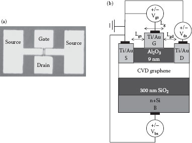
FIGURE 30.1 (a) RF transistor device micrograph in the G–S–G configuration. (b) Cross-sectional schematic and biasing conditions. Lg = Lsd = 1.5 mm and W = 75 mm.
Graphene on SiO2 substrates are cleaned with acetone/methanol/isopropanol, followed by a deionized water rinse and N2 dry. Samples are baked for 5 min at 125°C to accelerate the removal of solvent. AZ5214 photoresist is coated, and source/drain contact regions are patterned by image reversal. Then, the 5-nm Ti/100-nm Au is evaporated, and the substrates are soaked for 24 h in acetone, followed by liftoff using rinses in acetone/methanol/IPA/H2O. To minimize damage, lift-off is performed with gentle pipette rinsing and no ultrasonication. Following source/drain formation, graphene channels are patterned with AZ5214 and defined using a direct plasma etch (20-sccm O2/70 W). Substrates are solvent-cleaned, and an ~9 nm gate dielectric is deposited by plasma-assisted atomic layer deposition as reported in Ref. [7] directly into the graphene. The film thicknesses are determined from the spectroscopic ellipsometry and capacitance–voltage measurements of the identical films deposited on Si. Top gates are formed identical to the process for a source/drain. Figure 30.1a shows a top-down optical image of a constructed two gate-finger field-effect-transistor (FET) and Figure 30.1b shows a cross-sectional schematic of the device.
30.3 DEVICE ELECTRICAL MEASUREMENTS
The DC characteristics of constructed devices with a gate length Lg = 1.5 μm, gate-source/drain length Lsd = 1.5 μm, and width W = 75 μm are measured using a Keithley 4200 semiconductor parametric analyzer. Figure 30.2a shows representative transfer (Id vs. Vgs) characteristics, and Figure 30.2b shows output characteristics (Id vs. Vds). The characteristics are typical of devices produced using this CVD graphene and that incorporate the plasma-assisted Al2O3 gate dielectric, producing with a positive dirac point voltage Vdp that corresponds to an effectively heavily p-type “oxygen doped” film [7]. The transconductance gm = dId/dVgs and is shown in Figure 30.2c along with the total conductance gd = dId/dVds in Figure 30.2d. The FETs operate normally on “depletion mode,” and with increasing Vgs, there is gate-controlled modulation of the Fermi level that reduces the effective channel charge (hole) density and the overall Id. Owing to a density-dependent carrier mobility [2,3] observed for graphene synthesized by this method and using this dielectric [7], gm also increases with increasing Vgs and is 28 mS/mm with Vgs = 0 V/Vds = 4 V to 72 mS/mm with Vgs = 6 V/Vds = 4 V. With low Vds, the output characteristics are near ohmic due to good quality contacts. With increasing Vds, gds decreases from 260 to 160 mS/mm. The reduction in gds is due to the onset of saturation-like behavior. The origin of this behavior is still under examination and could be due to the slight band-gap opening with this dielectric. Strong saturation is required to significantly decrease gds and obtain significant intrinsic voltage gain for the devices [6].
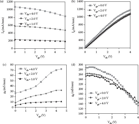
FIGURE 30.2 Measured (a) transfer Id versus Vgs characteristics representative of heavily p-type doped graphene due to the PA-ALD gate-dielectric process and (b) output (Id vs. Vds) characteristics showing signs of saturation with Vds + 3 V. (c) Extracted transconductance gm versus Vgs with weak modulation for 0 < Vgs < 2 V. (d) Conductance gd that increases with Vds due to onset of saturation-like effects.
Two-port RF measurements were taken in the ground–signal–ground (G-S-G) configuration and collected using an Agilent PNA sampling in the 10 MHz–50 GHz range. The current amplification h21, unilateral power gain (U), and Mason’s power gain (MSG) versus frequency are extracted from the collected S parameters for stable conditions and are shown in Figure 30.3a. The h21 and U characteristics follow a near-ideal −20 dB/dec behavior expected for good-quality ideal RF transistors. ft/fmax are ~3.2 GHz/1.8 GHz for Vgs = 5 V/Vds = 5 V, demonstrating both GHz current gain and maximum oscillation frequency. The increased frequency performance with increased Vgs is consistent with the increased gm observed in the DC measurements.
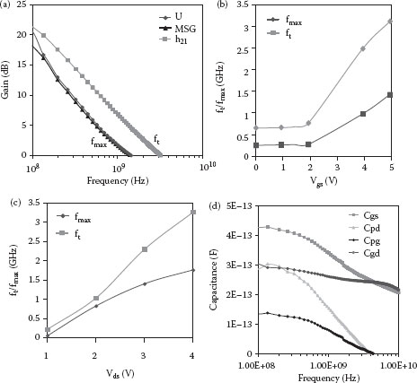
FIGURE 30.3 Measured (a) Mason’s unilateral gain (U), transducer gain (MAG), and current gain (h21) characteristics versus frequency. (b) The extracted ft and fmax as a function of Vgs in agreement with the gm characteristics and nearly constant over a 2 V range. (c) ft and fmax as a function of Vds. (d) Relevant extracted small-signal capacitances.
Figure 30.3b shows the dependence of ft and fmax as a function of Vgs. The behavior is consistent with the gm behavior. While the ft and fmax are not completely linear across the full 6 V window, there is not an apparent gm collapse that severely diminishes the frequency response due to graphene being able to sustain a significant charge density >1013 cm2/Vs. In fact, we find near-linear characteristics over the 2–3 V range, which could be favorable for linear RF circuits. Also, with reduced Vds, there is a more linear gm, which corresponds to less modulation of ft/fmax with Vgs.
30.4 SMALL-SIGNAL ANALYSIS AND DISCUSSION
The ft and fmax can depend significantly on the capacitances of both the intrinsic and extrinsic (including parasitic) parts of the transistor. To obtain further insight into performance-limiting factors and how to achieve an increased frequency performance device, conventional transistor small-signal models are used to extract the small-signal parameters of the intrinsic components Cgs, Cgd, as well as the extrinsic (parasitic) Cpg, Cpd. The small-signal gm, gd, and Rds are also extracted for comparison with the DC data. The capacitances are presented as a function of the frequency and are shown in Figure 30.3d. The parasitic elements are extracted using the admittance (Y) parameters obtained by converting from the scattering (S) parameters. Using the Y parameters, the following expressions are used that are derived from the equivalent conventional FET small-signal circuit [8]. As can be seen, the dominant capacitance is the intrinsic Cgs; however, the parasitic gate/drain pad capacitances are still large enough to limit the overall frequency/power performance.
Radiofrequency transistors based on CVD graphene and incorporating plasma-assisted atomic layer-deposited gate dielectric are constructed and examined. The DC characteristics for this process are representative of a heavily p-type doped graphene. The RF extrinsic ft (unity-gain frequency) and fmax (maximum oscillation frequency) are both in the GHz regime. The dependency of ft/fmax as a function of Vgs and Vds are consistent with the gm and Id dependencies. ft/fmax are near linear over a 2 V Vgs range, consistent with a near-constant gm for this operating region. The small-signal capacitances are extracted from conventional FET circuit models to determine the performance-limiting factors.
1. R. Piner, I. Velamakanni, E. Jung, E. Tutuc, S.K. Banerjee, L. Colombo, and R.S. Ruoff, Large-area synthesis of high-quality and uniform graphene films on copper foils, Science Express Reports, 324(5932), 1312–1314, 2009.
2. O.M. Nayfeh, Radio-frequency transistors using chemical-vapor-deposited monolayer graphene: Performance, doping, and transport effects, IEEE Transactions on Electron Devices, 58(9), 2847–2853, 2011.
3. O.M. Nayfeh, Graphene transistors on mechanically flexible polyimide incorporating atomic-layer-deposited gate dielectric, IEEE Electron Device Letters, 32(10), 1349–1351, 2011.
4. S-Ki Lee, B.J. Kim, H. Jang, S.C. Yoon, C. Lee, B.H. Hong, J.A. Rogers, J.Ho Cho, and J.-H. Ahn, Stretchable graphene transistors with printed dielectrics and gate electrodes, Nano Letters, 11(11), 4642–4646, 2011.
5. S. Bae, H.K. Kim, Y. B. Lee, X.F. Xu, J.S. Park, Y. Zheng, J. Balakrishnan et al., Roll-to-roll production of 30-inch graphene films for transparent electrodes, Nature Nanotechnology, 5, 574–578, 2010.
6. K. Kim, J-Y. Choi, T. Kim, S-H. Cho, and H-J. Chung, A role for graphene in silicon-based semiconductor devices, Nature, 479, 338–344, 2011.
7. O.M. Nayfeh, T. Marr, and M. Dubey, Impact of plasma-assisted atomic-layer-deposited gate dielectric on graphene transistors, IEEE Electron Device Letters, 32(4), 473–475, 2011.
8. J.G. Dambrine, A. Cappy, D. Heliodore, and E. Playez, A new method for determining the FET small-signal equivalent circuit, IEEE Transactions on Microwave Theory, 36(7), 1151–1159, 1988.