
Graphene-on-Diamond Devices and Interconnects Carbon sp2-on-sp3 Technology |
|
CONTENTS
31.2 Selection of Substrate Materials
31.4 Graphene Preparation and Characterization
31.5 Graphene Device Fabrication
31.6 Characteristics of Graphene-on-Diamond Devices
31.7 Thermal Breakdown in Graphene Devices
Graphene is a promising material for future electronics owing to its extremely high carrier mobility [1, 2 and 3], thermal conductivity [4,5], saturation velocity [2,3], and ability to integrate with almost any substrate [6]. The most feasible are applications that do not require a bandgap but can capitalize on graphene’s superior current-carrying capacity. Graphene field-effect transistors (FETs) and interconnects built on SiO2/Si substrates reveal the breakdown current density, JBR, of ~1 μA/nm2 [7, 8 and 9], which is ~100 × larger than the fundamental electromigration limit for the metals [10]. However, the current-carrying capacity of graphene-on-SiO2/Si devices is still smaller than the maximum achieved in carbon nanotubes (CNTs) [11, 12 and 13]. In this chapter, we outline the graphene-on-diamond technology, which enables the fabrication of graphene-on-diamond devices and interconnects with a substantially enhanced breakdown current density. The discussion in this chapter follows our report of a systematic study of the current-induced breakdown in graphene-on-diamond devices [14]. The study demonstrated that by replacing SiO2 with a synthetic diamond, one can solve the early-graphene-device-failure problem and increase JBR of graphene by an order of magnitude to above ~10 μA/nm2 [14]. We used recent advances in the chemical vapor deposition (CVD) and processing of diamond for fabricating >40 graphene devices on ultra-nanocrystalline diamond (UNCD) and single-crystal diamond (SCD) substrates with a surface roughness below δH ≈ 1 nm. It was found that not only SCD but also UNCD with a grain size D ~ 5–10 nm can improve JBR, owing to the increased thermal conductivity of UNCD at higher temperatures. The obtained results are important for graphene applications in interconnects [7,15] and radio-frequency transistors [16], and can lead to the new planar sp2-on-sp3 carbon-on-carbon technology.
31.2 SELECTION OF SUBSTRATE MATERIALS
Graphene devices are commonly fabricated on Si/SiO2 substrates with an SiO2 thickness of H ≈ 300 nm [1, 2 and 3]. Owing to optical interference, graphene becomes visible on Si/SiO2 (300-nm) substrates, which facilitates its identification. It was discovered that graphene has excellent heat conduction properties with the intrinsic thermal conductivity, K, exceeding 2000 W/mK at room temperature (RT) [4,5]. However, in typical device structures, for example, FETs or interconnects, most of the heat propagates directly below the graphene channel in the direction of the heat sink, that is, the bottom of the Si wafer [17,18]. For this reason, the highly thermally resistive SiO2 layers act as the thermal bottleneck, not allowing one to capitalize on graphene’s excellent intrinsic thermal properties. Theoretical considerations suggest that the breakdown mechanism in sp2-bonded graphene should be similar to that in sp2-bonded CNTs. Unlike in metals, the breakdown in CNTs was attributed to the resistive heating or local oxidation, assisted by defects [11, 12, 13 and 14]. Thermal conductivity of SiO2 K = 0.5–1.4 W/mK at RT [19] is more than 1000-times smaller than that of Si, K = 145 W/mK, which indicates that the use of materials with higher K, directly below graphene, can improve graphene’s JBR and reach the maximum values observed for CNTs.
Synthetic diamond is a natural candidate for use as a bottom dielectric in graphene devices, which can perform the function of a heat spreader. Recently, there was a major progress in CVD diamond growth performed at low temperature, T, compatible with Si complementary metal–oxide–semiconductor (CMOS) technology [20, 21 and 22]. There are other potential benefits of utilizing diamond thin films as substrates for graphene devices instead of SiO2. The energy of the optical phonons in diamond, Ep = 165 meV, is much larger than that in SiO2, Ep = 59 meV. The latter can improve the saturation velocity in graphene when it is limited by the surface electron—phonon scattering [23]. The lower trap density achievable in diamond, compared to SiO2, indicates a possibility of reduction of the 1/f noise in graphene-on-diamond devices [24], which is essential for applications in r.f. transistors and interconnects. It was also demonstrated that replacing SiO2 with diamond-like carbon (DLC) helps to substantially improve the radio frequency characteristics of the graphene transistors [16]. However, DLC is an amorphous material with K = 0.2–3.5 W/mK at RT [25], which is a low value even when compared to SiO2. Depending on the H content, as-deposited DLC films have high internal stress, which needs to be released by annealing at higher T ~ 600°C [26]. These facts provide strong motivations for the search of other carbon materials, which can be used as substrates for graphene devices.
Synthetic diamond can be grown in a variety of forms from UNCD films with the small grain size, D, and, correspondingly low K, to SCD, with the highest K among all bulk solids. Microcrystalline diamond (MCD) has larger D than UNCD but suffers from unacceptable surface roughness, δH, and high thermal boundary resistance, RB [5]. Up to date despite attempts in many groups to fabricate graphene devices on diamond with acceptable characteristics, no breakthrough was reported. The major stumbling blocks for the development of viable graphene-on-diamond sp2-on-sp3 technology are the high δH of synthetic diamond, difficulty of visualization of graphene on diamond, and problems with the top-gate fabrication—no bottom gates are possible on SCD substrates. The study reported in Ref. [14] used the most recent advances in CVD diamond growth and polishing as well as our experience of graphene device fabrication to prepare a large number of test structures, and study the current-carrying and thermal characteristics of graphene-on-diamond devices in the practically relevant ambient conditions. In this chapter, we discuss two main forms of diamond—UNCD and SCD—which represent two extreme cases in terms of D and K.
The examined UNCD films were grown on Si substrates in the microwave plasma chemical vapor deposition (MPCVD) system at the Argonne National Laboratory [14]. Figure 31.1a,b shows the MPCVD system used for the growth inside a clean room and schematic of the process, respectively. The growth conditions were altered to obtain a larger D, in the range 5–10 nm, instead of the typical grain sizes D ≈ 2–5 nm in UNCDs. This was done to increase K of UNCD without strongly increasing the surface roughness. In our investigation, we intentionally did not increase D beyond 10 nm or used MCD in order to keep δH in the range suitable for polishing. The inset shows a 100-mm UNCD/Si wafer.
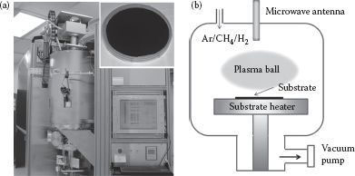
FIGURE 31.1 Synthetic diamond growth and characterization. (a) Large-area MPCVD system used for the synthetic diamond growth. The inset shows a 100-mm Si/UNCD wafer. (b) Schematics describing the UNCD growth in the MPCVD system.
The surface roughness of the synthetic diamond substrate plays an important role in reducing electron scattering at the graphene—diamond interface and increasing the electron mobility, μ. We performed the chemical mechanical polishing (CMP) to reduce the as-grown surface roughness from δH ≈ 4–7 nm to below δH ≈ 1 nm, which resulted in a corresponding reduction of the thickness, H, from the as-grown H ≈ 1 μm to ~700 nm. The H value was selected keeping in mind conditions for graphene visualization on UNCD, together with the thermal management requirements. The SCD substrates were type IIb (100) grown epitaxially on a seed diamond crystal and then laser cut from the seed. For graphene devices fabrication, the SCD substrates were acid washed, solvent cleaned, and put through the hydrogen termination process [27]. The near-edge x-ray absorption fine-structure spectroscopy (NEXAFS) of the grown UNCD film confirms its high sp3 content and quality (Figure 31.2a). The strong reduction of δH is evident from the atomic force microscopy (AFM) images of the as-grown UNCD and UNCD after CMP presented in Figure 31.2b and c, respectively.
31.4 GRAPHENE PREPARATION AND CHARACTERIZATION
Graphene and few-layer graphene (FLG) were prepared by exfoliation from the bulk highly oriented pyrolytic graphite (HOPG) to ensure quality and uniformity in thickness. We selected flakes of the rectangular-ribbon shape with the width W ≥ 1 μm, which is larger than the phonon mean free path (MFP) Λ in graphene [5]. The condition W > Λ ensured that K does not undergo additional degradation due to the phonon-edge scattering. The length, L, of graphene ribbons was in the range 10–60 μm. We selected ribbons with the small aspect ratio γ = W/L ~ 0.03–0.1 to imitate interconnects. Raman spectroscopy was used for determining the number of atomic planes, n, in FLG, although the presence of sp2 carbon at the grain boundaries in UNCD made the spectrum analysis more difficult. Figure 31.3a shows spectra of the graphene-on-UNCD/Si and UNCD/Si substrate. One can see the 1332 cm−1 peak, which corresponds to the optical vibrations in the diamond crystal structure. The peak is broadened due to the small D in UNCD. The bands at ~1170, 1500, and 1460 cm−1 are associated with the presence of trans-poly-acetylene and sp2 phase at grain boundaries [28,29]. The graphene G peak at 1582 cm−1 and 2D band at ~2700 cm−1 are clearly recognizable. Figure 31.3b presents spectra of the graphene-on-SCD and SCD substrate and the difference between the two. The intensity and width of the 1332 cm−1 peak confirms that we have a single-crystal diamond.
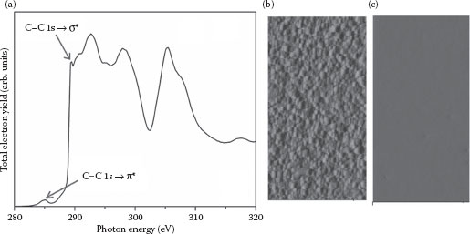
FIGURE 31.2 Material characterization of a synthetic diamond. (a) NEXAFS data for a deposited UNCD thin film revealing its high sp3 content and quality. The exciton peak at ~289.3 eV corresponds to 1s → σ* resonance from sp3 carbon. The peak at ~285 eV corresponds to 1s → π* resonance from sp2 carbon at grain boundaries. The revealed sp2 fraction is 2%, which is lower than the typical 5% sp2 content, owing to larger D in our UNCD. (b) and (c) AFM images of the as-grown and chemical–mechanical polished UNCD, respectively.
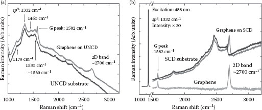
FIGURE 31.3 Micro-Raman spectroscopic analysis of graphene-on-diamond samples. (a) Raman spectra of graphene-on-UNCD (upper curve) and UNCD substrate (lower curve). (b) Raman spectra of graphene-on-SCD and SCD substrate. The difference in spectra (lower curve) was used to determine the number of atomic planes, n. The specific example shows a single-layer graphene. The data indicate that micro-Raman spectroscopy can be used for identification of graphene on synthetic diamond samples, which contain sp2 phase on grain boundaries.
31.5 GRAPHENE DEVICE FABRICATION
We focused our discussion on devices made of FLG with n ≤ 5. FLG supported on substrates or embedded between dielectrics preserves its transport properties better than single-layer graphene. Two-terminal (i.e., interconnects) and three-terminal (i.e., FETs) devices were fabricated on both UNCD/Si and SCD substrates. The electron-beam lithography (EBL) was used to define the source, drain contacts, and gate electrodes. The contacts consisted of a thin Ti film covered by a thicker Au film. The top-gate HfO2 dielectric was grown by the atomic layer deposition (ALD). The novelty in our design, as compared to the graphene-on-SiO2/Si devices, was the fact that the gate electrode and pad were completely separated by the HfO2 layer to avoid oxide lift-off sharp edges, which can affect the connection of the gate electrode.
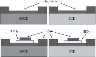
FIGURE 31.4 Schematic of the graphene-on-diamond devices showing the two-terminal and three-terminal devices fabricated for testing on UNCD/Si and SCD substrates.
Figure 31.4 shows schematics of the fabricated devices. For testing the breakdown current density in FLG, we used two-terminal devices in order to minimize extrinsic effects on the current and heat conduction. Three-terminal devices were utilized for μ measurements. We also fabricated conventional graphene-on-SiO2/Si devices as references. Figure 31.5 is an optical microscopy image of two-terminal graphene-on-SCD devices. Figures 31.6a and b show the scanning electron microscopy (SEM) images of the two-terminal and three-terminal graphene-on-UNCD devices, respectively. We electrically characterized >40 graphene-on-diamond devices and +10 graphene-on-SiO2/Si reference devices [14]. To understand the origin of the breakdown, we correlated JBR values with the thermal resistances of the substrates. We measured the effective K of the substrates and determined their thermal resistance as RT = HS/K, where HS is the substrate thickness.
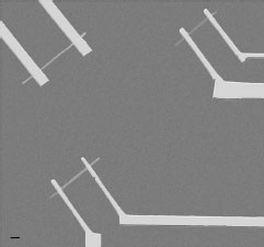
FIGURE 31.5 Optical microscopy image of the two-terminal graphene devices—prototype interconnects—on a single-crystal synthetic diamond.
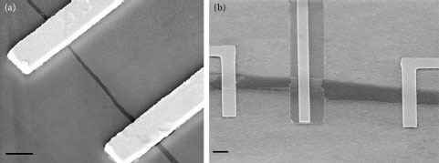
FIGURE 31.6 SEM images of the two-terminal (i.e., interconnects) and three-terminal (i.e., transistors) graphene-on-UNCD/Si devices. (a) The two-terminal devices were used for the breakdown current density testing. (b) The three-terminal devices were utilized to measure the mobility. The scale bar is 2 μm.
31.6 CHARACTERISTICS OF GRAPHENE-ON-DIAMOND DEVICES
Figure 31.7a shows RT for the UNCD/Si and Si/SiO2 (300 nm) substrates as a function of T. Note that RT for Si increases approximately linearly with T, which is expected because the intrinsic thermal conductivity of crystalline materials decreases as K ~ 1/T for T above RT. The T dependence of RT for UNCD/Si is completely different, which results from the interplay of heat conduction in UNCD and Si. In UNCD, K grows with T owing to the increasing inter-grain transparency for the acoustic phonons that carry heat [5]. UNCD/Si substrates, despite being more thermally resistive than Si wafers at RT, can become less thermally resistive at high T. The RT value for SCD substrate is ~0.25 × 10⁻⁶ m2K/W, which is more than an order of magnitude smaller than that of Si at RT. The thermal interface resistance, RB, between FLG and the substrates is RB ≈ 10−8 m2K/W, and it does not depend strongly on either n or the substrate material [5]. For this reason, RB does not affect the RT trends.
Figure 31.7 shows the current–voltage (I −V) characteristics of graphene-on-SCD FET at low source–drain voltages for different top-gate, VTG, bias. The inset demonstrates a high quality of the HfO2 dielectric and metal gate deposited on top of the graphene channel. The linearity of I–Vs confirms that the contacts are Ohmic. Figure 31.8a presents the source–drain, ISD, current as a function of VTG for graphene-on-UNCD FET. In the good top-gate graphene-on-diamond devices, the extracted μ was ~1520 cm2/V/s for the electrons and ~2590 cm2/V/s for the holes. These mobility values are acceptable for applications in downscaled electronics. In Figure 31.8b, we show results of the breakdown testing. For graphene-on-UNCD, we obtained JBR ≈ 5 × 10⁸ A/cm2 as the highest value, while the majority of devices broke at JBR ≈ 2 × 10⁸ A/cm2. The reference graphene-on-SiO2/Si had JBR ≈ 108 A/cm2, which is consistent with the literature [7, 8 and 9]. The maximum achieved for graphene-on-SCD was as high as JBR ≈ 1.8 × 10⁹ A/cm2. This is an important result, which shows that via improved heat removal from graphene channel one can reach, and even exceed, the maximum current-carrying capacity of ~10 μA/nm2 (= 1 × 10⁹ A/cm2) reported for CNTs [11, 12, 13 and 14]. The surprising improvement in JBR for graphene-on-UNCD is explained by the reduced RT at high T where the failure occurs. At this temperature, RT of UNCD/Si can be lower than that of Si/SiO2.
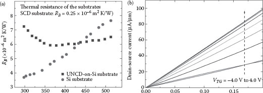
FIGURE 31.7 Electrical and thermal characteristics of graphene-on-diamond. (a) Thermal resistance of a UNCD/Si substrate and a reference Si wafer. Note that the thermal resistance of the composite UNCD/Si substrate decreases at the high temperature. (b) Low-field I −V characteristics of top-gate graphene-on-SCD devices. (The figure is based on the experimental data reported in Yu J. et al., Nano Lett., 12, 1603, 2012.)
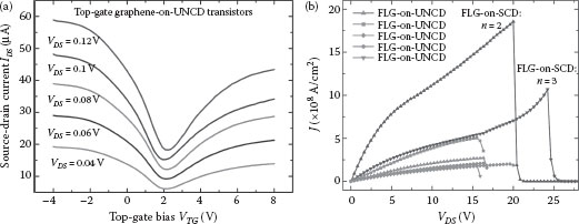
FIGURE 31.8 Breakdown current testing of graphene-on-diamond devices. (a) The source–drain current in the three-terminal graphene-on-UNCD devices as a function of the top-gate bias. (b) The breakdown current density in the two-terminal graphene-on-UNCD and graphene-on-SCD devices. Note an order of magnitude improvement in the current-carrying ability of graphene devices and interconnects fabricated on the single-crystal synthetic diamond. (The figure is based on the experimental data reported in Yu J. et al., Nano Lett., 12, 1603, 2012.)
31.7 THERMAL BREAKDOWN IN GRAPHENE DEVICES
The location of the current-induced failure spot and JBR dependence on electrical resistivity, ρ, and length, L, can shed light on the physical mechanism of the breakdown. The failures in the middle of CNTs and JBR ~ 1/ρ were interpreted as signatures of the electron diffusive transport, which resulted in the highest Joule heating in the middle [11, 12 and 13]. The failures at the CNT-metal contact were attributed to the electron ballistic transport through CNT and energy release at the contact. There is a difference in contacting CNT with the diameter d ~ 1 nm and graphene ribbons with W ≥ 1 μm. It is easier to break CNT-metal than the graphene-metal contact thermally. In our study, we observed the failures both in the middle and near the contact regions (see Figure 31.9). The difference between these two types was less pronounced than that in CNTs. The failures occurred not exactly at the graphene–metal interface but at some distance, which varied from sample to sample. We attributed it to the width variations in graphene ribbons leading to breakdowns in the narrowest regions, or in the regions with defects, which are distributed randomly. We did not observe scaling of JBR with ρ as we did in the case of CNTs.
The breakdown current density, JBR, for graphene scaled well with ρL. Figure 31.9 shows data for graphene-on-UNCD with a similar aspect ratio. From the fit to the experimental data, we obtained JBR = α(ρL)−β, where α = 1.3 × 10⁻⁶ and β = 0.73. For graphene-on-SCD, the slope is β = 0.51. Previously, the scaling with (ρL)−β (where β = 0.6–0.7) was observed in carbon nanofibers (CNF) [30], which had a similar aspect ratio. Such JBR(ρL) dependence was explained from the solution of the heat-diffusion equation, which included thermal coupling to the substrate. However, the thermally induced JBR for CNF was ~106 A/cm2—much smaller than the record JBR ≈ 1.8 × 10⁹ A/cm2 we obtained for graphene-on-SCD.
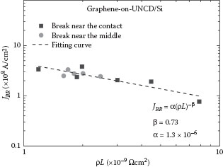
FIGURE 31.9 Scaling of the breakdown current density. JBR as a function of the electrical resistance and length of graphene interconnects. The device failures close to the middle of the graphene channel and to the graphene—metal contact are indicated with the circles and rectangles, respectively. (The figure is based on the experimental data reported in Yu J. et al., Nano Lett., 12, 1603, 2012.)
We described a possibility of a substantial increase in the current-carrying capacity of graphene devices and interconnects via their fabrication on synthetic diamond substrates. The obtained results are important for the proposed graphene applications in interconnects and radiofrequency transistors, and can eventually lead to the new planar sp2-on-sp3 carbon-on-carbon technology.
The work at the University of California at Riverside was supported by the Office of Naval Research (ONR) through award N00014-10-1-0224, Semiconductor Research Corporation (SRC) and Defense Advanced Research Project Agency (DARPA) through the FCRP Center on Functional Engineered Nano Architectonics (FENA), and DARPA Defense Microelectronics Activity (DMEA) under agreement number H94003-10-2-1003. The work at the Argonne National Laboratory was supported by the U.S. Department of Energy (DOE), Office of Science and Office of Basic Energy Sciences under Contract DE-AC02-06CH11357. NEXAFS studies were performed at the University of Wisconsin Synchrotron Radiation Center.
1. Novoselov, K. S. et al. Electric field effect in atomically thin carbon films. Science 306, 666–669, 2004.
2. Novoselov, K. S. et al. Two-dimensional gas of massless Dirac fermions in graphene. Nature 438, 197–200, 2005.
3. Zhang, Y. B., Tan, Y. W., Stormer, H. L., and Kim, P. Experimental observation of the quantum Hall effect and Berry’s phase in graphene. Nature 438, 201–204, 2005.
4. Ghosh, S. et al. Dimensional crossover of thermal transport in few-layer graphene. Nat. Mat. 9, 555, 2010.
5. Balandin, A. A. Thermal properties of graphene and nanostructured carbon materials. Nat. Mat. 10, 569–581, 2011.
6. Palacios, T. Graphene electronics: Thinking outside the silicon box. Nat. Nano. 6, 464–465, 2011.
7. Murali, R. et al. Breakdown current density of graphene nanoribbons. Appl. Phys. Lett. 94, 243114, 2009.
8. Yu, T. et al. Bilayer graphene system: Current-induced reliability limit. IEEE Electron Device Lett. 31, 1155–1157, 2010.
9. Lee, K. J., Chandrakasan, A. P., and Kong, J. Breakdown current density of CVD-grown multilayer graphene interconnects. IEEE Electron Device Lett. 32, 557–559, 2011.
10. Christou, A. Electromigration and Electronic Device Degradation (Wiley-Interscience, New York, NY, 1994).
11. Collins, P. G., Hersam, M., Arnold, M., Martel, R., and Avouris, P. Current saturation and electrical breakdown in multiwalled carbon nanotubes. Phys. Rev. Lett. 86, 3128, 2001.
12. Tsutsui, M. et al. Electrical breakdown of short multiwalled carbon nanotubes. J. Appl. Phys. 100, 094302, 2006.
13. Huang, J. H. et al. Atomic scale imaging of wall-by-wall breakdown and concurrent transport measurements in multiwall carbon nanotubes. Phys. Rev. Lett. 94, 236802, 2005.
14. Yu, J., Liu, G., Sumant, A. V., Goyal, V., and Balandin, A. A. Graphene-on-diamond devices with increased current-carrying capacity: Carbon sp2-on-sp3 technology. Nano Lett., 12, 1603, 2012.
15. Shao, Q., Liu, G., Teweldebrhan, D., and Balandin, A. A. High-temperature quenching of electrical resistance in graphene interconnects. Appl. Phys. Lett. 92, 202108, 2008.
16. Wu, Y. et al. High-frequency scaled graphene transistors on diamond-like carbon. Nature. 472, 74–78, 2011.
17. Freitag, M. et al. Energy dissipation in graphene field-effect transistors. Nano Lett. 9, 1883–1888, 2009.
18. Subrina, S., Kotchetkov, D., and Balandin, A. A. Heat removal in silicon-on-insulator integrated circuits with graphene lateral heat spreaders. IEEE Electron Device Lett. 30, 1281, 2009.
19. Yamane, T. et al. Measurement of thermal conductivity of silicon dioxide thin films using a 3Ω method. J. Appl. Phys. 91, 9772, 2002.
20. Sumant, A. V. et al. Ultrananocrystalline and nanocrystalline diamond thin films for MEMS/NEMS applications. MRS Bull. 35, 281, 2010.
21. Sumant, A. V. et al. Large area low temperature ultrananocrystalline diamond films and integration with CMOS devices for monolithically integrated MEMS/NEMS-CMOS systems. Proc. SPIE 7318, 17, 2009.
22. Goldsmith, C. et al. Charging characteristics of ultrananocrystalline diamond in RF-MEMS capacitive switches. IEEE Intl. Microwave Symp. Dig. 1246–1249, 2010. DOI: 10.1109/MWSYM.2010.5517781.
23. Meric, I. et al. Current saturation in zero-bandgap, top-gated graphene field-effect transistors. Nat. Nanotechnol. 3, 654–659, 2008.
24. Liu, G. et al. Low-frequency electronic noise in the double-gate single-layer graphene transistors. Appl. Phys. Lett. 95, 033103, 2009.
25. Shamsa, M. et al. Thermal conduction in diamond-like carbon thin films. Appl. Phys. Lett. 89, 161921, 2006.
26. Friedmann et al. Thick stress-free amorphous tetrahedral carbon films with hardness near that of diamond. Appl. Phys. Lett. 71, 3820, 1997.
27. Sumant, A. V. et al. Correlation between surface chemistry and nanotribology for ultrananocrystalline diamond, and application to micro- and nanomechanical systems. Phys. Rev. B 76, 235429, 2007.
28. Ferrari, A. C. and Robertson, J. Origin of the 1150-cm−1 Raman mode in nanocrystalline diamond. Phys. Rev. B 63, 121405, 2001.
29. Shamsa, M. et al. Thermal conductivity of nitrogenated ultrananocrystalline diamond films on silicon. J. Appl. Phys. 103, 083538, 2008.
30. Suzuki, M. et al. Current-induced breakdown of carbon nanofibers. J. Appl. Phys. 101, 114307, 2007.