
Graphene Band Gap Modification via Functionalization with Metal-Bis-Arene Molecules |
CONTENTS
32.3.2 Possible Synthesis Strategy
Graphene continues to draw immense interest because of its unusual electronic and spin properties resulting from a simple structure composed of a single layer of carbon atoms arranged in a two-dimensional honeycomb pattern [1,2]. These properties, including the ballistic carrier transport and quantum Hall effect, make it a promising candidate as a building block of future nanoelectronic devices and as a possible replacement for silicon [3,4]. In spite of graphene’s amazing properties, there are some obstacles that need to be overcome before it can be considered as a viable candidate to replace silicon. The main barrier is the absence of a band gap. Therefore, producing a band gap is probably one of the most important challenges that must be addressed before graphene can ultimately enable practical applications ranging from digital electronics to infrared nanophotonics.
A number of possible solutions have been proposed and demonstrated for producing band gaps in single- and double-layered graphene. One of the more straightforward methods involves the growth of epitaxial graphene on a lattice-matched (SiC) substrate to induce a stress and, as a result, open up a band gap of about 0.26 eV [5]. Alternatively, a somewhat more successful method utilizes quantum confinement to open a band gap in graphene by the fabrication of nanoscale structures, that is, quantum dots and nanoribbons, where the band gap varies inversely with the nanoscale structure dimension [6, 7 and 8]. However, the nonuniform edges of these structures play a major role in degrading their electrical properties [9]. For example, with graphene nanoribbon of widths less than 10 nm, a band gap of about 0.4 eV has been reported; however, associated electron motilities are between 100 and 200 cm2/V.s. Mobility is believed to be degraded by edge scattering [10].
A graphene bilayer shares many of the interesting properties of a single-layered film and provides a richer band structure, albeit without a band gap. Theoretical studies have predicted that a significant band gap could be induced by breaking the inversion of the two layers through the application of a perpendicular electric field [11, 12 and 13]. Using a single or double (top and bottom) gates to apply a strong electric field, a tunable band gap of up to about 250 meV has been created in graphene field effect transistors [14,15].
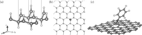
FIGURE 32.1 View of the molecular structures of functionalized graphene. (a) Hydrogenated graphene. (Adapted from K. Suggs, D. Reuven and X.-Q. Wang, Journal of Physical Chemistry C, 115, 3313–3317, 2011.) (Adapted from D. K. Samarakoon and X.-Q. Wang, ACS Nano, 4, 4126–30, 2010.) (b) With metal adatom (Fe). (Adapted from A. V. Krasheninnikov et al., Physical Review Letters, 102, 126807, 2009.) (c) Perfluorophenylazide (PFPA)-functionalized graphene.
Chemical modification of graphene by covalently functionalizing its surface potentially allows a wider flexibility in engineering electronic structure, in particular the local density of states of the carbon atoms bound to the modifier that can result in the opening of the band gap. Such binding can involve covalent hydrogenation of graphene to modify hybridization of carbon atoms from sp2 to sp3 geometry as shown in Figure 32.1a [16, 17 and 18]. Methods have also been developed to functionalize graphene covalently with molecular species and adatoms (Figure 32.1b) [19, 20, 21, 22, 23 and 24]. Among these, perfluorophenylazide (PFPA) functionalization of graphene is well developed using a nitrene intermediate (Figure 32.1c). We have utilized films of this molecule to act as adhesion layers to produce long ribbons of exfoliated graphene [21, 22, 23 and 24].
To minimize the effects of edge scattering of carriers, wider strips of graphene would be required for the fabrication of devices; however, these wider strips will be semimetallic. Therefore, our objective is to identify molecules that, when covalently bonded to graphene, can break its conical band structure and open up an energy gap. To achieve this goal, we have examined the electronic structure of metal-arene (MA)-functionalized graphene and report below our results based on the first-principles density-functional calculations of the band gap-functionalized graphene (MA-Gr). It is shown that the MA covalently binds at the π-conjugation of graphene and changes the electronic properties from metallic to semiconducting. We also show that the energy gap can be tuned by adjusting the number of bound MA adducts.
During our previous investigation of utilizing PFPA as an adhesion layer, it was determined that PFPA was covalently bonded to graphene [21]. Hence, we first simulated the covalent binding energy and the resulting induced band gap in graphene of PFPA and its derivatives. (For the calculation methods, see below.) Derivatives that were considered were obtained by substituting the nitrogen in the nitrene radical by the element listed in Table 32.1. It can be seen that the widest gap of 0.24 eV induced in graphene is when it is functionalized with a single PFPA molecule per 6 × 6 graphene supercell. Functionalization with two molecules slightly increases the gap to 0.28 eV. This gap is not wide enough for the fabrication of practical devices. Therefore, we next focused on MA-functionalized graphene.
TABLE 32.1
Band Gaps of PFPA-Functionalized Graphene
![]()
a Nonzero values below 0.001 Ha (~0.027 eV) cannot be calculated exactly and are therefore set to approximate zero.
The calculations were conducted within the framework of the density functional theory (DFT) as implemented in the DMol3 package [27]. The generalized gradient approximation (GGA) in BLYP [28,29] exchange-correlation parameterization was used for both final geometry optimization and band structure calculation. Initial geometry optimization was performed using the local density approximation (LDA) with the Vosko–Wilk–Nusair (VWN) [30] correlation function. A 6 × 6 graphene supercell with a vacuum space of 11.5 Å normal to the graphene plane was used. The geometry optimization convergence criterion was satisfied when the total energy change was less than 3 × 10⁻⁵ Ha. Only one k-point (gamma) was used throughout the calculations since the distance between neighboring k-points was only 0.077 1/Å due to a large supercell choice. For the band structure computation, the k-path selected was Γ–M–K–Γ, with 24, 20, and 40 k-points on each segment correspondingly. Although the GGA approach systematically underestimates the band gaps, we are primarily interested in the mechanism of a gap opening. For that purpose, the GGA approach is expected to provide qualitatively correct information. A more precise GW approach is very costly with this system, consisting of a total of 94 atoms. The DMol3 package utilizes a numerical orbital basis set for the radial part of the wave function centered on the atoms. This allows one to include a thick vacuum layer into the model without increase of the computation time.
To pursue the effect of adduct concentration on the electronic structures, we have considered two configurations by adding one or four MA molecules onto a 6 × 6 rhombus cell, respectively. The cell constitutes 72 carbon atoms of graphene and 1 metal, 6 carbon, and 6 hydrogen atoms of each MA molecule.
Various studies conducted on adatoms of transition metals on graphene and CNTs have demonstrated a broad potential for modifying the electronic structure of graphene [25,26,31,32]. Partially filled d-shells can play the role of electron donors [33], disturbing the π-conjugated system and thus possibly opening a gap. However, it was found that a single transition element adatom produces an insignificant charge transfer of ~0.01 electrons per carbon atom from the transition metal to the graphene sheet, and thus hardly changes the band structure [34]. Even so, “sandwich compounds” such as metallocenes and bis-arenes have long been known and are of great interest in inorganic chemistry. Moreover, it is well known that ligand aromaticity is preserved in these compounds; therefore, replacing one of the aromatic ligands with a graphene sheet would seem to be an attractive method for functionalization since
1. Metallocenes and metal-bis-arene compounds are known to be good electronic donors [35] and graphene shows the strongest interaction with electron donor and acceptor molecules via molecular charge transfer [36].
2. The geometrical structure of η6 compounds is similar to the honeycomb structure of graphene.
Based on these observations, we undertook a study of MA-functionalized graphene for the following 3d metals: Ti, V, Cr, Mn, and Fe (Zn and Cu have a closed 3d shell and are therefore ignored) in two different configurations—one and four MA molecules per 6 × 6 graphene supercell (Figure 32.2).
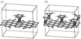
FIGURE 32.2 Ball-and-stick presentation of optimized structures of MA-functionalized graphene (top view) with one (a) and four (b) MA adducts per 6 × 6 graphene supercell.
MA produces very strong bonds with the graphene sheet. The binding energy of Cr-MA was found by extrapolating to 0 K of the binding energies obtained by Hess’s law for different values of thermal occupancy smearing. A quite high value of this energy of −4.72 eV (455.41 kJ/mol), which is about 25 kJ/mol per electron, indicates strong bonding and presents a solid evidence for the real existence of such compounds.
32.3.2 POSSIBLE SYNTHESIS STRATEGY
MA complexes are known to exist for all transition metals [37], and their structure and chemistry resemble that of metallocenes. One of the many possible ways of synthesis is condensation of metal vapors on graphene, followed by aromatic molecules such as benzene at low temperature and pressure. Elschebroich and Kündig [38,39] have successfully applied this strategy to polyaromatics, which leads us to believe that this conventional synthesis approach may allow us to produce MA-functionalized graphene sheets. Varying the concentration of metal vapor and aromatic molecules could provide a means to achieve a different degree of functionalization.
We summarize in Table 32.2 the optimized configuration of MA-functionalized graphene.
TABLE 32.2
Geometrical Parameters of Free MA Molecules and MA Molecules Bound to the Graphene Sheet
Metal atom |
Ti |
V |
Cr |
Mn |
Fe |
∠(C–M–C) (°) (MA) |
103.477 |
101.397 |
99.76 |
101.285 |
104.353 |
M–C(a) (A) |
2.312 |
2.255 |
2.211 |
2.244 |
2.314 |
∠(C–M–C) (°) (1 mol) |
105.411 |
101.433 |
101.183 |
99.748 |
97.475 |
M–C(a)/M–C(g) (A) |
2.361/2.368 |
2.295/2.310 |
2.235/2.266 |
2.171/2.266 |
2.186/2.358 |
∠(C–M–C) (°) (4 mol) |
105.346 |
102.886 |
100.991 |
100.198 |
102.835 |
M–C(a)/M–C(g) (A) |
2.335/2.391 |
2.26/2.334 |
2.216/2.274 |
2.161/2.298 |
2.198/2.394 |
Source: (P. Plachinda, D. Evans, and R. Solanki, Modification of graphene band structure by haptic functionalization, 2011 11th IEEE Conference on Nanotechnology (IEEE-NANO), Aug. 15–18, pp.1187–1192. © (2011) IEEE. With permission.)
TABLE 32.3
Electronic Configuration of the Metal Atoms in the MA, and the Corresponding Energy Gap Opening in the MA-Gr as a Result of Functionalization
Metal atom |
Ti |
V |
Cr |
Mn |
Fe |
Number of valence electrons |
16 |
17 |
18 |
19 |
20 |
Electronic configuration: |
|||||
↑ |
↑↑ |
||||
↑ |
↓↑ |
↓↑ |
↓↑ |
||
e2g (x²–y², xy) |
↓↑↓↑ |
↓↑↓↑ |
↓↑↓↑ |
↓↑ ↓↑ |
↓↑↓↑ |
Number of unpaired electrons |
0 |
1 |
0 |
1 |
2 |
Eg (1 molecule) (eV) |
0.40815 |
0.10884 |
0.38094 |
0.29931 |
0 |
Eg (4 molecule) (eV) |
0.32652 |
0.78909 |
0.8163 |
0 |
0.48978 |
Source: (P. Plachinda, D. Evans, and R. Solanki, Modification of graphene band structure by haptic functionalization, 2011 11th IEEE Conference on Nanotechnology (IEEE-NANO), Aug. 15–18, pp.1187–1192. © (2011) IEEE. With permission.)
As can be seen from Table 32.2, the bonding to an “infinite” graphene sheet changes the structural features with respect to the free M[η6-(arene)2] molecule. General trends in the bonding lengths demonstrate the following features: the M–C (graphene) bond lengths remain about 3% longer than the one in the free molecule; the M–C (arene) bonds, however, remain almost unchanged with respect to the free molecules for Ti–Cr metals and become about 3% shorter for Mn and Fe. The reason for the extreme behavior of the bond lengths can be explained by considering a molecular orbital representation of the MAs. The usage of molecular orbitals (instead of Wannier functions as for a periodic system) is justified because we assume little interaction between the molecules from the neighboring cells. In the Cr[η6-(arene)2], electrons fully occupy the a1g binding orbital, whereas adding additional electrons, as happens in Mn and Fe, leads to partial population of the antibonding, twice degenerate orbital, which is composed of the 4p and 4s atomic orbitals of the metal and antibonding π*-orbitals of graphene and arene (see Table 32.3).
The conjugated π-system of the graphene sheet can effectively redistribute additional electron density donated by the metal atom, and thus decrease the number of electrons on the M–C (graphene) bond, thus weakening it. Deviation from the single-molecule behavior for the M–C (arene) bond (Figure 32.3a) is hardly observed for Ti, V, and Cr. Mn and Fe compounds, as mentioned above, demonstrate about 3% shortening of the bond. We relate this distortion to the Jahn–Teller effect: unpaired electrons in the Mn and Fe compounds occupy a doubly degenerate level, and therefore the Mn and Fe compounds undergo geometrical distortion that removes degeneracy. This asymmetry in bond length also leads to the difference in the C (arene)–M–C (graphene) angles: for Ti–Cr, they exceed those for the free molecule, but for Mn–Fe, they are less. This phenomenon results in less mixing of the localized atomic d-orbitals and leads to the creation of narrow bands in the band structure of MA-Gr, decreasing the band gap compared to the corresponding Ti–Cr compounds.
The graphene–metal interaction in haptic functionalization has direct consequences on the electronic properties of graphene. As previously reported, the functionalization of graphene with radical (primarily hydrogen, epoxide, and nitrene) groups locally disrupt the planarity of the graphene sheet, changing the local hybridization from sp2 to sp3 geometry [16, 17 and 18], which induces an sp3-type defectlike state near the Fermi level. (Hereinafter, under the Fermi level in insulators, we understand the top of the valence band, where it is conventionally put by the majority of the DFT programs.) In our case, however, the graphene sheet is not distorted in the z-direction and thus rehybridization of carbon atoms does not occur. The local bonding configuration is, however, significantly affected by the electronic structure of the functionalizing atom, and especially its d-electrons that were found to lie close to the Fermi level. This is similar to the situation with sp3-type “impurity” states for radical functionalization. Partially occupied, highly localized d-orbitals near the Fermi level cause repulsion of the π-bands, causing the energy band of pristine graphene to be shifted away from the Fermi level due to the π–d interaction.
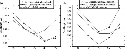
FIGURE 32.3 Geometrical parameters of the MA-Gr. (a) M–C (arene) bond length. (b) M–C (graphene) bond length. (P. Plachinda, D. Evans, and R. Solanki, Modification of graphene band structure by haptic functionalization, 2011 11th IEEE Conference on Nanotechnology (IEEE-NANO), Aug. 15–18, pp. 1187–1192. © (2011) IEEE. With permission.)
The calculated band structures for CrBA-functionalized graphene are compared with pristine graphene in Figure 32.4. It is readily observable that after haptic functionalization, the linear dispersion law of pristine graphene at the Dirac point is entirely broken. Since the calculations were conducted using a 6 × 6 supercell, the K point maps to the Γ point, due to the folding of the reciprocal space. The π- and π*-bands in the Γ direction in pristine graphene have a separation of about 11.26 eV. The bands that were previously intersecting at the Dirac point are now shifted together at the new Γ point of the supercell. The π- and π*-bands preserve their arrangement in the functionalized graphene; however, the distance between them grows from about 1 eV in 1-MA-Gr to 1.25 eV in 4-MA-Gr. (This growth is attributed to the shift of the π*-band by +0.25 eV relative to the 1-MA-Gr.) As the analysis of the density of states calculated for different atoms and projected on different angular momenta demonstrates, a system of pure (with no π-admixture) localized d-bands of the metal is now located between the π- and π*-bands of graphene, preventing them from crossing. These d-bands cause a strong repulsion and are responsible for the opening of the gap now between the bands produced by the metal. These electronic properties of MA-functionalized products are in contrast to the sp3 rehybridization and loss of π-electrons found upon the addition of acceptor chemical groups or metals in other functionalization schemes [15,25,40]. The fact that the band gap strongly depends on the nature of the functionalizing metal atom confirms our idea about the importance of the number of d-electrons or the modification of the band structure. Both occupied and empty d-levels of the metal form flat bands close to the Fermi level. These “impurity” states are probably responsible for bringing the strongest contribution to the band repulsion, more than the d-admixture of the former pure π- and π*-bands. Additional flat d-bands produced by the localized electrons of the metal atoms in the MA-Gr can be successfully utilized to mimic dopant levels of conventional semiconductors.
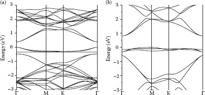
FIGURE 32.4 Calculated band structures for one single-molecule CrBA-functionalized graphene (a) and four-molecule CrBA-functionalized graphene (b). (P. Plachinda, D. Evans, and R. Solanki, Modification of graphene band structure by haptic functionalization, 2011 11th IEEE Conference on Nanotechnology (IEEE-NANO), Aug. 15–18, pp. 1187–1192. © (2011) IEEE. With permission.)
An important property of the MA-induced perturbation of the band structure is that alteration in the electronic structure of graphene increases with the increasing MA functionalization concentration. We have investigated the functionalization of graphene at a higher adduct concentration by including three more MA functional groups in the unit cell (see Figure 32.2). Owing to the limitations imposed by the nature of the DFT calculations, we cannot study the variation of the electronic properties imposed by continuously changing the concentration of functionalizing molecules. This would require dealing with huge supercells. Two aforementioned geometries correspond to one functionalizing molecule per 6 × 6 and 3 × 3 graphene supercells. An important idea is to demonstrate the ability to tweak the band gap by varying the concentration, possibly even in the broader limits than discussed here. This corresponds to one MA molecule per 3 × 3 graphene supercell. The exact positions of functionalizing molecules inside the unit cell are not important since there are many ways to redefine the lattice. This geometry is further labeled as 4-MA-Gr unlike 1-MA-Gr with only one MA per 6 × 6 graphene supercell. As the concentration of functionalizing molecules increases (i.e., by transition from 1-MA-Gr to 4-MA-Gr), repulsion between the π-bands (graphene) increases as well, leading to a wider band opening. The extracted energy gap is 0.44 and 0.98 eV for one and four CrBA adducts (i.e., CrBA-Gr and 4-GrBA-Gr), respectively, on a graphene unit cell consisting of 72 graphene-carbon atoms. A higher number of d-bands complicates the picture. The distance between the π-bands in 1-VBA-Gr at the Γ-point is about 0.8 eV but “impurity” levels decrease it 10 times to 0.08 eV. The distance between the d-levels in 1-MnBA-Gr is about 2.7 eV, which is much more than the distance between the π-bands; thus, the highest occupied molecular orbital (HOMO) and the lowest unoccupied molecular level (LUMO) of 1-MnBA-Gr line up with the π- and π*-bands of graphene. As the number of electrons in the system increases, the Fermi level drifts up, causing a transition from a semiconducting to a metallic state. The band alignments of 1-MnBA-Gr and 1-FeBA-Gr are almost the same; however, owing to the extra electron of Fe, the Fermi level becomes coincident with the former π*-band, making the iron compound semimetallic. The same trend is observed in transition from 4-MnBA-Gr to 4-FeBA-Gr. The latter becomes metallic for the very same reason: since the Fermi level is located higher in the iron compound, it becomes metallic despite its very close similarity to the band alignment between 4-MnBA-Gr and 4-FeBA-Gr. The band diagrams of all substances under consideration are presented in Figure 32.5.
A closer analysis of band alignment demonstrates that a gap opening can be primarily attributed to the interaction of the d-electrons with the π-conjugated system. Although the carbon atoms on graphene connecting to MA essentially retain a flat band configuration corresponding to sp2 hybridization, additional π–d interaction is nevertheless present. Local modification of the original π-conjugation in the vicinity of the metal atom is manifested by rehybridization, that is, the HOMO and the LUMO of MA-Gr now are formed by the π-backbonding [41] mechanism. This rehybridization, however, is in contrast to conventional sp2 → sp3 rehybridization because it occurs without a major geometrical distortion of the underlying graphene sheet. Accordingly, carrier scattering can be substantially regarded as being due to electrostatic interaction similar to that observed for ionized dopant impurities in conventional semiconductors rather than due to localized defect states. As a consequence, it is to be expected that mobility degradation will be much less in MA-Gr than in covalently functionalized graphene for which significant nonplanarity of the graphene sheet is unavoidable. Indeed, this is a crucial difference and was the original motivation for considering this type of functionalization since it seems rather obvious that the preservation of aromaticity, viz., sp2 hybridization, should result in less degradation of carrier transport properties. Of course, this must be confirmed experimentally and work in that direction is in progress.
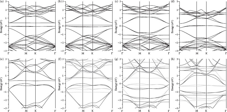
FIGURE 32.5 Band structures of 1-MA-Gr (a–d) and 4-MA-Gr (e–h), where M = Ti (a,e), V (b,f), Mn (c,g), and Fe (d,h). Solid and dashed lines correspond to the spin-up and spin-down bands. Energy reference level coincides with the position of the Fermi level. (P. Plachinda, D. Evans, and R. Solanki, Modification of graphene band structure by haptic functionalization, 2011 11th IEEE Conference on Nanotechnology (IEEE-NANO), Aug. 15–18, pp. 1187–1192. © (2011) IEEE. With permission.)
The charge densities of the corresponding HOMO/LUMO at the band center (the Γ point) are shown in Figure 32.5. Different atoms demonstrate different mixing of atomic orbitals that take part in the formation of HOMO and LUMO. The HOMO of 1-CrBA-Gr and 1-MnBA-Gr (not shown) are constructed by the σ-type donation mechanism (empty d-orbital is interacting with the filled π-orbital). The LUMO of these compounds and 1-VBA-Gr, in turn, demonstrate π-type back-donation behavior (filled d-orbital interacts with an empty π*-orbital). The HOMO of 1-VBA-Gr is entirely represented by the orbital of the metal atom. The MO picture of the 1-iron is somewhat different from that of the other atoms: π-type back-donation for HOMO and the σ-type donation for LUMO. This is to be contrasted with 4-MA functionalization. As can be seen in Figure 32.6, an increase of adduct concentration impedes the donation mechanism causing the HOMOs of 4-Cr to consist of the unhybridized orbitals of the metal atom and the LUMO of the π-type back-donation MOs.
Molecular orbitals of other MA-Gr structures are not shown here due to space limitations. However, the donation mechanism changes depending on the number and energy of the filled d-orbitals of the central atom. A proportional increase of functionalizing molecules causes a change in the amount of π-conjugated bonds broken due to the backbonding mechanism. This correlates with the associated increase of the band gap and thus provides support for the suggested scenario of the d-level-induced band gap opening.
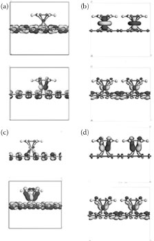
FIGURE 32.6 Molecular orbitals (HOMO—top row, LUMO—bottom row) for 1-CrBA-Gr (a), 4-CrBA-Gr (b), 1-FeBA-Gr (c), and 4-FeBA-Gr (d).
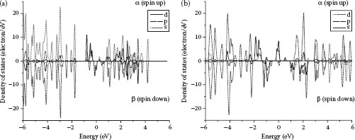
FIGURE 32.7 (a) Spin-resolved density of states in 4-VMB-Gr. (b) Spin-resolved density of states in 4-FeMB-Gr.
As was previously demonstrated, graphene functionalized with transition metal atoms can demonstrate profound magnetic properties [25]. Band structures of 4-VBA-Gr and 4-FeBA-Gr (Figures 32.7a and 32.7b) demonstrate strong spin polarization. Spin-unrestricted calculations reveal significant differences between the spin-up (α) and spin-down (β) densities of states (DoS) pointing to ferromagnetic behavior of 4-VMB-Gr and 4-FeMB-Gr.
Iron demonstrates an even stronger difference in the DoS for the spin-up and spin-down electrons. Band structures for compounds with different central metal atoms having paired electrons obviously do not demonstrate any ferromagnetic behavior. However, owing to the presence of unpaired electrons, the manganese compound can exist in both ferromagnetic and antiferromagnetic states. A closer analysis of the magnetic properties of the MA-Gr will be published separately. The presence of a nontrivial magnetic structure suggests wide possible applications of the MA-functionalized graphene in spintronics.
We have studied the electronic characteristics of MA-functionalized graphene and have shown that the MA adducts mainly preserve the sp2 hybridization network of the carbons on graphene away from the functionalizing groups. However, the π-conjugation of graphene near the Fermi level is greatly modified by the π-backbonding process, caused by d-orbitals of the metal atom in the functionalizing molecule, which leads to the opening of a substantial band gap dependent upon the adduct concentration and number of the occupied d-orbitals. Band gaps vary from 0.81 eV for 4-CrBA-Gr to 0.11 eV for 1-VBA-Gr, and to zero for 1-FeBA-Gr and 4-MnBA-Gr. Moreover, the electronic structure of the functionalizing metal in the MA molecules allows the possibility of controlled modification of both the band gap itself and the position of the Fermi level with respect to the “d-impurity” levels and native graphene bands. Some functionalizing molecules result in a ferromagnetic behavior along with the opening of the band gap. Such dependence of the electronic properties on the type of functionalizing metal suggests a novel tunable approach for the “band engineering” of graphene. Our findings on the nature of an MA-functionalization-induced band gap provide useful guidelines for enabling the flexibility and optimization of graphene-based nanodevices.
1. A. K. Geim and K. S. Novoselov, The rise of graphene, Nature Materials, 6, 183–91, 2007.
2. M. J. Allen, V. C. Tung, and R. B. Kaner, Honeycomb carbon: A review of graphene, Chemical Reviews, 110, 132–145, 2010.
3. C. Rao, A. Sood, K. Subrahmanyam, and A. Govindaraj, Graphene: The new two-dimensional nanomaterial, Angewandte Chemie International Edition, 48, 7752–7777, 2009.
4. A. H. C. Neto, F. Guinea, N. M. R. Peres, K. S. Novoselov, and A. K. Geim, The electronic properties of graphene, Review of Modern Physics, 81, 109–162, 2009.
5. V. M. Pereira, A. H. Castro Neto, and N. M. R. Peres, Tight-binding approach to uniaxial strain in graphene, Physical Review B, 80, 045401, 2009.
6. B. Trauzettel, D. V. Bulaev, D. Loss, and G. Burkard, Spin qubits in graphene quantum dots, Nature Physics, 3, 192–196, 2007.
7. K. Nakada, M. Fujita, G. Dresselhaus, and M. S. Dresselhaus, Edge state in graphene ribbons: Nanometer size effect and edge shape dependence, Physical Review B, 54, 17954, 1996.
8. L. Brey and H. A. Fertig, Electronic states of graphene nanoribbons studied with the Dirac equation, Physical Review B, 73, 235411, 2006.
9. K. A. Ritter and J. W. Lyding, The influence of edge structure on the electronic properties of graphene quantum dots and nanoribbons, Nature Materials, 8, 235–242, 2009.
10. X. Li, X. Wang, L. Zhang, S. Lee, and H. Dai, Chemically derived, ultrasmooth graphene nanoribbon semiconductors, Science, 319, 1229–1232, 2008.
11. E. V. Castro, K. S. Novoselov, S. V. Morozov, N. M. R. Peres, J. M. B. L. dosSantos, J. Nilsson, F. Guinea, A. K. Geim, and A. H. CastroNeto, Biased bilayer graphene: Semiconductor with a gap tunable by the electric field effect, Physical Review Letters, 99, 216802, 2007.
12. E. McCann, Asymmetry gap in the electronic band structure of bilayer graphene, Physical Review B, 74, 161403, 2006.
13. Y. Zhang, T.-T, Tang, C. Girit, Z. Hao, M. C. Martin, A. Zettl, M. F. Crommie, Y. R. Shen, and F. Wang, Direct observation of a widely tunable bandgap in bilayer graphene, Nature, 459, 820–823, 2009.
14. K. F. Mak, C. H. Lui, J. Shan, and T. F. Heinz, Observation of an electric-field-induced band gap in bilayer graphene by infrared spectroscopy, Physical Review Letters, 102, 256405, 2009.
15. D. K. Samarakoon and X.-Q. Wang, Tunable band gap in hydrogenated bilayer graphene, ACS Nano, 4, 4126–30, 2010.
16. D. C. Elias, R. R. Nair, T. M. G. Mohiuddin, S. V. Morozov, P. Blake, M. P. Halsall, A. C. Ferrari et al., Control of graphene’s properties by reversible hydrogenation: Evidence for graphane, Science, 323, 610–613, 2009.
17. O. Leenaerts, B. Partoens, and F. M. Peeters, Hydrogenation of bilayer graphene and the formation of bilayer graphane from first principles, Physical Review B, 80, 245422, 2009.
18. M. Z. S. Flores et al., Graphene to graphane: A theoretical study, Nanotechnology, 20, 465704, 2009.
19. J. Choi, K.-j. Kim, B. Kim, H. Lee, and S. Kim, Covalent functionalization of epitaxial graphene by azidotrimethylsilane, The Journal of Physical Chemistry C, 113, 9433–9435, 2009.
20. M. Quintana, K. Spyrou, M. Grzelczak, W. R. Browne, P. Rudolf, and M. Prato, Functionalization of graphene via 1,3-dipolar cycloaddition, ACS Nano, 4, 3527–3533.
21. L.-H. Liu and M. Yan, Simple method for the covalent immobilization of graphene, Nano Letters, 9, 3375–3378, 2009.
22. L.-H. Liu, G. Zorn, D. G. Castner, R. Solanki, M. M. Lerner, and M. Yan, A simple and scalable route to wafer-size patterned graphene, Journal of Materials Chemistry, 20, 5041–5046, 2010.
23. L.-H. Liu, M. M. Lerner, and M. Yan, Derivitization of pristine graphene with well-defined chemical functionalities, Nano Letters, 10, 3754–3756.
24. L.-H. Liu, G. Nandamuri, R. Solanki, and M. Yan, Electrical properties of covalently immobilized single-layer graphene devices, Journal of Nanoscience and Nanotechnology, 11, 1288–1292, 2011.
25. A. V. Krasheninnikov, P. O. Lehtinen, A. S. Foster, P. Pyykko, and R. M. Nieminen, Embedding transition-metal atoms in graphene: Structure, bonding, and magnetism, Physical Review Letters, 102, 126807, 2009.
26. K. Suggs, D. Reuven, and X.-Q. Wang, Electronic properties of cycloaddition-functionalized graphene, Journal of Physical Chemistry C, 115, 3313–3317, 2011.
27. DMol3. San Diego, CA: Accelrys Software Inc., 2010.
28. A. D. Becke, Density-functional exchange-energy approximation with correct asymptotic behavior, Physical Review A, 38, 3098, 1988.
29. C. Lee, W. Yang, and R. G. Parr, Development of the Colle-Salvetti correlation-energy formula into a functional of the electron density, Physical Review B, 37, 785, 1988.
30. S. H. Vosko, L. Wilk, and M. Nusair, Accurate spin-dependent electron liquid correlation energies for local spin density calculations: A critical analysis Canadian Journal of Physics, 58, 1200–1211, 1980.
31. Ishii, M. Yamamoto, H. Asano, and K. Fujiwara, DFT calculation for adatom adsorption on graphene sheet as a prototype of carbon nanotube functionalization, Journal of Physics: Conference Series, 100, 052087, 2008.
32. K. Suggs, D. Reuven, and X.-Q. Wang, Electronic properties of cycloaddition functionalized graphene, The Journal of Physical Chemistry C, 115(8), 3313–3317, 2011.
33. V. Zólyomi, Á. Rusznyák, J. Koltai, J. Kürti, and C. J. Lambert, Functionalization of graphene with transition metals, Physica Status Solidi (B), 247(11–12), 2920–2923, 2010.
34. O. Leenaerts, B. Partoens, and F. M. Peeters, Paramagnetic adsorbates on graphene: A charge transfer analysis, Applied Physics Letters, 92, 243125, 2008.
35. R. L. Brandon, J. H. Osiecki, and A. Ottenberg, The reactions of metallocenes with electron acceptors 1a, The Journal of Organic Chemistry, 31, 1214–1217, 1966.
36. C. N. R. Rao, K. S. Subrahmanyam, H. S. S. Ramakrishna Matte, B. Abdulhakeem, A. Govindaraj, B. Das, P. Kumar, A. Ghosh, and D. J. Late, A study of the synthetic methods and properties of graphenes, Science and Technology of Advanced Materials, 11, 054502, 2010.
37. D. Astruc, Chapter 11: Metallocenes and sandwich complexes, in Organometallic Chemistry and Catalysis Berlin: Springer, 2007, pp. 251–288.
38. C. Elschenbroich and R. Möckel, Bis(η6-naphthalin)chrom(0), Angewandte Chemie, 89, 908–909, 1977.
39. E. P. Kundig and P. L. Timms, Metal atom preparation and ligand displacement reactions of bisnaphthalenechromium and related compounds, Journal of the Chemical Society, Chemical Communications, pp. 912–913, 1977.
40. S. M.-M. Dubois, Z. Zanolli, X. Declerck, and J.-C. Charlier, Electronic properties and quantum transport in Graphene-based nanostructures, The European Physical Journal B, 72, 1–24, 2009.
41. A. D. McNaught and A. Wilkinson, IUPAC. Compendium of Chemical Terminology, 2nd ed. (The Gold Book). Oxford: Blackwell Scientific Publications, 2006.
42. P. Plachinda, D. Evans, and R. Solanki, Modification of graphene band structure by haptic functionalization, 2011 11th IEEE Conference on Nanotechnology (IEEE-NANO), Aug. 15–18, pp. 1187–1192.