
CONTENTS
34.2 Current-to-Voltage Conversion Method
34.2.1 Resistor-Based Current Readout Method
34.2.2 Capacitor-Based Current Readout Method
34.3 Design of Sensor Readout System
34.3.1 Zero Bias Current-to-Voltage Conversion
34.4.1 Hardware Setup of Testing System
34.5 Application of Readout System
34.5.1 Readout in Single Pixel Camera
An optoelectronic device includes all studies and applications on electronic devices that source, detect, and control light. Through the detectors, light signal will be converted to an electrical signal and then be processed by a voltage monitoring or current monitoring circuit. In wide bandwidth light, infrared (IR) light was extensively used from military to nonmilitary purposes. There are thousands of commercialized applications in industrial, scientific, and medical areas, including hyperspectral imaging in biological and mineralogical measurements; target acquisition and tracking, night vision in military applications [1]; IR data communications by standards published by IrDA; IR telescope in astronomy; environment monitoring in meteorology, and so on. It is also closely related to the human body, because humans at normal temperature can radiate around 12 μm wavelength IR light based on Wien’s displacement law.
In all IR imaging systems, it was mainly composed of optical components, including lens, mirrors, and IR sensors. The typical IR sensors, including the FPA, QD, and QW structures [2,3], are temperature dependent and work under very low temperatures in order to maintain high efficiency. Experimentally, it is shown that carbon nanotube (CNT)-based IR sensors perform well at room temperature [4]. Our group studied the noncryogenic cooled CNT-based IR imaging system in detail.
However, the photocurrent is from a pico-ampere to a nano-ampere in a CNT IR sensor [5,6] and it is bias dependent. To read photocurrent in the CNT IR sensor and to integrate the sensor into the imaging system, a low-noise, high-gain readout circuit is needed. As shown in Figure 34.1, a fully current readout system for the CNT-based IR sensor includes a sensor, a current-to-voltage module, and a digital signal processing module (DSP).
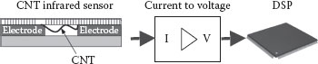
FIGURE 34.1 Current readout system for the CNT IR sensor.
To distinguish the voltage difference on the photodetector, it must generate at least a millivoltscale voltage when light irradiates on the detector. While the photovoltaic effect is not as great as a silicon photodiode in a CNT-based IR detector [6, 7 and 8], it can generate a nanoampere-scale photocurrent without voltage changes. However, in current monitoring circuits, for the purpose of reducing the bias voltage influence on photodetectors, it requires that readout circuits implement zero input impedance. In a in CNT-based IR detector especially, the photocurrent characteristic greatly depends on the applied bias voltage [7,8]. There are two requirements of readout circuits of a CNT-based IR detector: one relates to the high resolutions to the picoamperescale, the other is no bias application on the detector. To get a good resolution, a high-performance current-to-voltage amplifier (also named the trans-impedance amplifier) becomes the most important module in the readout system.
34.2 CURRENT-TO-VOLTAGE CONVERSION METHOD
There are two types of CNT detector signal monitoring, including voltage monitoring and current monitoring. Voltage monitoring requires a great voltage difference (at least mV scale) on the detector, when light irradiates on the detector. In CNT detector experiments [9], the CNT photovoltaic effect is not like a silicon photodiode; it generates a nanoampere scale photocurrent while the voltage does not change much. However, current monitoring requires that the readout circuits present zero input impedance to the detector, and the readout circuit absorbs the detector’s current without producing a voltage across the detector, especially for a CNT-based detector, in which the photocurrent characteristic of a CNT detector depends on the applied bias voltage. It is the best way to use zero bias for current monitoring on the CNT detector.
34.2.1 RESISTOR-BASED CURRENT READOUT METHOD
To convert pA/nA photocurrent to voltage, a current-to-voltage amplifier (also named a trans-impedance amplifier) becomes the most important module in a readout system; then a microprocessor can be used to process the photocurrent. The basic principle of a current-to-voltage converter (IV converter) is to use photocurrent (Ip) multiplied by a resistor. These circuits, shown in Figure 34.2, need very large (approximately GΩ) and precise resistors to detect pA currents [10]. The thermal noise of a large resistor will also limit the resolution of the circuit. The deep negative feedback of the amplifier (OPA1) makes the negative node (−) and positive node (+) work in the same potential, so the CNT detector is at zero bias in this condition.
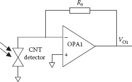
FIGURE 34.2 Schematic of the R type IV converter.
34.2.2 CAPACITOR-BASED CURRENT READOUT METHOD
A capacitive trans-impedance amplifier (CTIA) works as a current-to-voltage converter (IV converter) and it also can be designed to have high charge-to-voltage conversion ratios and low read noise [10,11]. Figure 34.3 is the basic circuit of a CTIA using a switch capacitor as the adjust resistor. There are two working phases in Figure 34.3. In phase 1, switch S is high, a OPA2 works like a voltage follower. The CNT detector forms a circular loop with current source in OPA2 and the photocurrent is a partial current of the current source. In phase 2, switch S is low in Toff seconds, the photocurrent (Ip) will charge a negative node (−) of OPA2, and the charge will redistribute in it. Q = Ip*Toff. VO2 = Q/C0 (Toff represents switch S off time). This circuit can detect as low current as possible based on the noise process in the input and was used in our readout system. It also achieves a large power supply rejection ratio (PSRR), a high open-loop gain, and a large dynamic range. The CTIA gain is given by G = Q/C0, QIN being the input charge integrated on the CTIA’s feedback capacitor.
34.3 DESIGN OF SENSOR READOUT SYSTEM
34.3.1 ZERO BIAS CURRENT-to-VOLTAGE CONVERSION
There are two requirements of readout circuits of a CNT-based IR detector: one is the high resolution to a picoampere scale; the other is no bias or bias modulation on the detector. To reduce noise and read such low current of an MWCNT detector, a capacitive transimpedance amplifier, shown in Figure 34.3, was designed in this IR readout system, because CTIA have high charge-to-voltage conversion ratios and low read noise [11].
The amplifier works in deep negative feedback control, which will make bias on a CNT detector modulated by the positive input of OPA2 as shown in Figure 34.3. The circuit can detect low currents because of the input noise reduction.
In high-resolution ADC, Delta-sigma (ΔΣ; or sigma-delta, ΣΔ) modulation is a method for encoding high-resolution signals into lower-resolution signals using pulse-density modulation. A high performance, 24-bit Σ-Δ analog-to-digital converter (ADC) was used in our experiments. It combines wide input bandwidth and high speed with the benefits of Σ-Δ conversion with a performance of 106 dB SNR at 625 kSPS, making it ideal for high-speed data acquisition. A wide dynamic range, combined with significantly reduced anti-aliasing requirements, simplifies the design process. In addition, the device offers programmable decimation rates, and the digital FIR filter can be adjusted if the default characteristics are not appropriate to the application. It is ideal for applications demanding high SNR without a complex front-end signal processing design. Figure 34.4 shows the ADC part in a readout system, including the ADC control part, ADC chip, input, and out interface [9].
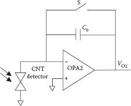
FIGURE 34.3 Schematic of the C type IV converter. (L. Chen et al., Readout system design for MWCNT infrared sensors, IEEE Nano Conference, Portland, Oregon, pp. 1635–1638. © (2011) IEEE. With permission.)
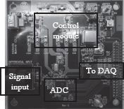
FIGURE 34.4 ADC PCB board in a readout system. (L. Chen et al., Readout system design for MWCNT infrared sensors, IEEE Nano Conference, Portland, Oregon, pp. 1635–1638. © (2011) IEEE. With permission.)
34.4.1 HARDWARE SETUP OF TESTING SYSTEM
In this section, the hardware setup and some experiment results of ROIC are presented. For the sake of reducing the noise after CTIA, a low-pass filter (LPF) was used to limit the bandwidth and optimize the thermal noise contribution on CTIA. Meanwhile, the LPF can weaken all highfrequency noise, including the power frequency noise. The readout system also includes ADC circuits, which were used to convert analog current to digital values. Figure 34.5 is the experimental PCB of a readout system.
On the basis of this readout system, a group of experiments were conducted to verify the performance of stability. In Figure 34.6, the x-axis corresponds to laser intensity. The digital output at T = 1 h maintains almost the same value at T = 0 with a different laser input. Meanwhile, the readout was also compared with a Curve Tracer (Agilent 4155C Semiconductor Analyzer) measurement in Figure 34.7. The results show that the readout system can reach pA resolution and has good stability performance [9].
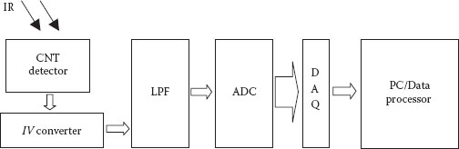
FIGURE 34.5 Diagram of a readout system.
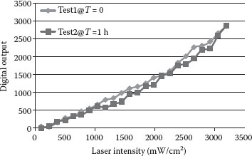
FIGURE 34.6 Readout test on CNT-based IR detector.
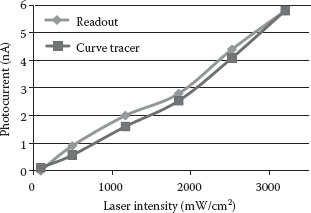
FIGURE 34.7 Compare readout system with Curve Tracer. (L. Chen et al., Readout system design for MWCNT infrared sensors, IEEE Nano Conference, Portland, Oregon, pp. 1635–1638. © (2011) IEEE. With permission)
34.5 APPLICATION OF READOUT SYSTEM
34.5.1 READOUT IN SINGLE PIXEL CAMERA
At last the readout system was also integrated in an MWCNT-based single pixel imaging system [12]. The hardware setup was shown in Figure 34.8, IR irradiation was controlled by DMD, and a lens was used to focus all IR light on the detector [9].
Based on the hardware, three groups of experiments were conducted. A rectangle bar was moved from the top to the bottom, where the recovery image can follow an objective image. The result shows that the lower left corner is destructive. From these results, we find that the readout system can work in the MWCNT IR single imaging system (Figure 34.9).
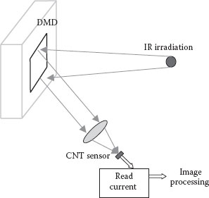
FIGURE 34.8 CNT-based single pixel IR imaging system.
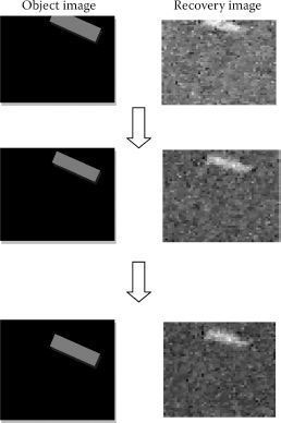
FIGURE 34.9 Recovery image based on a single MWCNT detector.
The design and experimental results of an MWCNT-based IR detector ROIC system are presented in this study. By this system, we can use it to test the low current to a sub-nanoampere in the CNT-based IR detector; it also works in the CNT-based single pixel IR imaging system. Although in our readout system it can work at a hundred Hertz, it is not enough for high-resolution image recovery. Meanwhile, an ultra-fast readout method is also a challenge project in nanoelectronics.
This research study is partially supported under NSF Grants IIS-0713346 and ONR Grants N00014-04-1-0799 and N00014-07-1-0935.
1. F. Szmulowicz, G. J. Brown, H. C. Liu et al., GaAs/AlGaAs p-type multiple quantum wells for infrared detection at normal incidence: Model and experiment, Opto Electronics Review, 9, 164–173, 2001.
2. M. Kolahdouz, A. A. Farniya, L. D. Benedetto, and H. H. Radamson. Improvement of infrared detection using Ge quantum dots multilayer structure, Applied Physics Letters, 96, 2135161–2135163, 2010.
3. A. Dehe, H. L. Hartnagel, D. Pavlidis, K. Hong, and E. Kuphal. Properties of InGaAs/InP thermoelectric and surface bulk micro machined infrared sensors, Applied Physics Letters, 69, 3039–3041, 1996.
4. I. A. Levitsky and W. B. Euler, Photoconductivity of single-wall carbon nanotubes under continuouswave near infrared illumination, Applied Physics Letters, 83, 1857–1859, 2003.
5. J., N. Xi, H. Chen, K. W. C. Lai, G. Li, and U. C. Wejinya, Design, manufacturing, and testing of single carbon nanotube based infrared sensors, IEEE Transactions on Nanotechnology, 8(2), 245–251, 2009.
6. J. Zhang, N. Xi, K. W. C. Lai, H. Chen, and Y. Luo, Single carbon nanotube based photodiodes for infrared detection, Proceedings of the 7th IEEE International Conference on Nanotechnology, 8(2), pp. 1156–1160, 2009.
7. J. Zhang, N. Xi, H. Chen, K. W. C. Lai, G. Li, and U. Wejinya, Photovoltaic effect in single carbon nanotube-based Schottky diodes, International Journal of Nanoparticles, 1(2), 108–118, 2008.
8. H. Chen, N. Xi, K. W. C. Lai, C. K. M. Fung, and R. Yang, Development of infrared detectors using single carbon nanotubes based field effect transistors, IEEE Transaction on Nanotechnology, 5(9), 582–589, 2010.
9. L. Chen, N. Xi, H. Chen, and K. W. C. Lai, Readout system design for MWCNT infrared sensors, IEEE Nano Conference, Portland, Oregon, pp. 1635–1638, 2011.
10. J. G. Graeme, Photodiode Amplifiers, OP Amp Solutions, McGraw-Hill Press, New York, pp. 23–30, 1995.
11. B. Fowler, J., D. How, and M. Godfrey. Low FPN high gain capacitive transimpedance amplifier for low noise CMOS image sensors, Proceedings of the SPIE, Vol. 4306, San Jose, CA.
12. M. F. Duarte, M. A. Davenport, D. Takhar et al., Single pixel imaging via compressive sampling, IEEE Signal Processing Magazine, pp. 83–92, 2008.